FPGA & CPLD
Products (6358)

EP4CE30F29I8L - 28.8K Logic Elements Cyclone IV E FPGA | Intel
The Intel (Altera) EP4CE30F29I8L is a Cyclone IV E family field-programmable gate array (FPGA) housed in a 780-ball fine-line BGA (FBGA-780) package, integrating 28,848 logic elements and 608,256 bits of embedded memory into a single low-power silicon platform. The part is rated for the industrial temperature range (-40C to +85C), runs from a 1.2 V core supply with separate 2.5 V/3.0 V/3.3 V auxiliary rails, and supports up to 532 user I/O pins across eight I/O banks with hot-socketing and PCI Express (PIPE) hard IP blocks. A field-programmable gate array (FPGA) is a semiconductor integrated circuit whose digital logic, interconnect, and routing are defined by a user-loaded configuration bitstream rather than at the factory. In the system hierarchy it sits between ASICs (Application-Specific Integrated Circuits) and general-purpose CPUs: an ASIC offers the highest performance-per-watt for a fixed function, while an FPGA trades silicon efficiency for in-system reprogrammability, parallel hardware execution, and time-to-market advantages. The Cyclone IV E family targets cost-sensitive volume applications where the flexibility of programmable logic outweighs the per-unit cost savings of a custom ASIC. Key features include 28,848 logic elements organized into 1,803 logic array blocks (LABs), 608 Kbits (66,528 bytes) of embedded RAM, 66 embedded 18x18 multipliers (DSP blocks), four general-purpose PLLs, and 20 global clock networks. The 8-input adaptive logic module (ALM) plus 9 Kbit M9K memory blocks give a balanced logic-to-memory ratio suited to digital signal processing, control, and glue-logic functions. The architecture combines an SRAM-based configuration fabric with on-chip DSP blocks, dual-purpose LVDS-compatible I/O, and hardened memory controllers, allowing designers to implement custom datapaths, bus bridges, and video/industrial interfaces without external glue logic. Configuration is loaded via JTAG, active serial (AS), or passive parallel (PP) modes from a low-cost serial flash. Typical applications include industrial motor control and machine vision, video processing and display bridges, telecommunications line cards, automotive driver assistance platforms, and PCI Express endpoint cards. The combination of high logic density, embedded multipliers, and PCI Express hard IP makes the EP4CE30F29I8L especially suitable for mid-volume, mid-complexity designs. When designing with this device, respect the 1.2 V core power-up sequencing requirement (VCCINT before VCCA/VCCIO) and provide a 100 MHz reference clock to any PLL used for DDR/PCIe. Decoupling must follow the Quartus Prime power distribution network guidelines for FBGA-780, and configuration mode pins (MSEL) must be tied correctly for AS x1/x4 or JTAG boot. This page synthesizes distributor pricing, drop-in alternatives, and practical design notes not found in the manufacturer datasheet alone.
EP4CE30F29I8LN - Cyclone IV E FPGA, 28K LE, 780-BGA | Intel
The Intel (formerly Altera) EP4CE30F29I8LN is a Cyclone IV E family field-programmable gate array (FPGA) housed in a 780-ball FineLine BGA package (29 mm body). The device integrates 28,848 logic elements, 532 user I/O pins, and 608,256 bits of embedded memory, delivering a cost-optimized programmable logic fabric for high-volume, low-power designs. What is an FPGA? A field-programmable gate array is a semiconductor device built around an array of configurable logic blocks (CLBs), programmable routing, and dedicated hard IP such as block RAM, DSP blocks, and PLLs. FPGAs sit between fixed-function ASICs and software-programmable processors in the design hierarchy: they provide hardware-level parallelism and timing determinism that microcontrollers cannot match, while remaining reprogrammable in the field. The Cyclone IV E family specifically targets low static power consumption (typically under 1.5 W at full utilization) and uses a TSMC 60 nm process node. Key features of the EP4CE30F29I8LN include 66 embedded 18 x 18 multipliers for DSP operations, 4 general-purpose PLLs for clock management, and support for external memory interfaces including DDR/DDR2 SDRAM and QDRII SRAM. The device operates from a 1.2 V core supply with PLL and I/O banks requiring 2.5 V to 3.3 V, and offers hot-socketing capability for in-system configuration. The Cyclone IV E architecture pairs a logic-rich fabric with hard PCIe Gen1 x4 IP and a configuration controller that supports JTAG (IEEE 1149.1), Active Serial (AS), and Passive Serial (PS) modes. The I8 speed grade and -40C to +100C industrial temperature range make this OPN (Ordering Part Number) suited to industrial, telecom, and test-and-measurement equipment. Typical applications for the EP4CE30F29I8LN include industrial motor control, LED video wall drivers, software-defined radio baseband pre-processing, machine vision pre-processing pipelines, and PCI Express endpoint cards in cost-sensitive embedded systems. Designers choose this OPN when 28K logic elements are sufficient and a 780-BGA footprint is acceptable for high-density I/O. When designing with the EP4CE30F29I8LN, allocate at least eight PCB layers for the 780-BGA breakout and follow Intel's Pin Connection Guidelines to tie unused pins to defined logic levels. Decouple every VCCINT and VCCA pin with 0.1 uF and 10 uF capacitors placed as close as possible to the package balls to meet the simultaneous-switching-noise (SSN) budget. This page synthesizes distributor pricing, drop-in alternative OPNs from the same Cyclone IV E family, and practical PCB layout notes that go beyond what the manufacturer datasheet alone provides, supporting faster component selection and BOM validation.

EP4CE40F19A7N - Cyclone IV E 39.6K LE FPGA, 193 I/O, 324-BGA | Altera
The Intel (Altera) EP4CE40F19A7N is a Cyclone IV E family Field-Programmable Gate Array (FPGA) with 39,600 logic elements, 1,161,216 bits of embedded memory, and 116 embedded multipliers, housed in a 324-ball FineLine BGA (F19) package. The device integrates 193 user I/O pins, four general-purpose PLLs, and a 60nm low-power process operating from a 1.0V core with 1.2V/2.5V/3.3V programmable I/O standards (LVTTL, LVCMOS, LVDS, SSTL, PCI). A Field-Programmable Gate Array (FPGA) is a reconfigurable semiconductor belonging to the hierarchy of programmable logic devices (PLD) -> complex PLD (CPLD) -> FPGA -> logic IC -> integrated circuit. FPGAs are used as flexible digital logic platforms that combine parallel hardware datapaths with on-chip memory, multipliers, and high-speed transceivers, enabling system designers to implement custom processors, glue logic, DSP pipelines, and protocol bridges without fabricating an ASIC. Key features include 113,560 adaptive logic modules (ALMs) equivalent to 39,600 classic logic elements (LE), 4 PLLs with fractional-n synthesis, embedded RAM of 1,161,216 bits organized as 244 M9K blocks (32,256 bits each) plus 1 MLAB block, and 116 18x18 hardware multipliers for DSP. The part operates from a single 1.0V core supply plus 2.5V/3.3V auxiliary supplies, with industrial temperature grade (TA = -40C to +125C equivalent for A7 suffix) and 60nm process technology that lowers static power versus prior Cyclone generations. Architecturally the device is built on a 60nm SRAM-based fabric with configuration stored in flash-less volatile memory (requires external configuration device such as EPCS or EPCQ). The Cyclone IV E architecture separates logic array blocks, memory blocks, multiplier blocks, and I/O element (IOE) banks; each IOE supports programmable slew rate, bus hold, weak pull-up, and on-chip termination (OCT) for signal integrity at LVDS/SSTL speeds. Typical applications include industrial motor control, video processing pipelines, machine vision, factory automation controllers, low-cost ASIC prototyping, automotive infotainment pre-production, and embedded DSP for medical imaging. With 116 multipliers and ample block RAM, the EP4CE40 is well-suited to finite impulse response (FIR) filters, FFT engines, and H.264 base-profile encoders at SD resolutions. When designing, plan configuration scheme carefully: choose between Active Serial (AS), Passive Serial (PS), JTAG, and Fast Passive Parallel (FPP) modes. Provide a clean multi-rail power sequence (1.0V VCCINT before or coincident with VCCAUX/VCCIO). Reserve decoupling to within 100 mils of each VCCINT pin and add a low-ESR bulk cap of at least 22uF. This page synthesizes distributor pricing, drop-in alternatives, and practical design notes not found in the manufacturer datasheet alone.

EP4CE40F23A7N - Cyclone IV E FPGA 39.6K LE | Intel (Altera)
The Intel (formerly Altera) EP4CE40F23A7N is a low-power, high-volume Cyclone IV E Field-Programmable Gate Array (FPGA) integrating 39,600 logic elements and 1,161,216 bits of embedded memory in a 484-ball FineLine BGA (FBGA-484) package. The device operates from a 1.2 V core supply, supports automotive-grade temperature ranges, and is fabricated on a low-power 60 nm process that targets cost-sensitive logic integration, parallel I/O expansion, and bridge applications. A Field-Programmable Gate Array (FPGA) is a semiconductor device built around an array of configurable logic blocks (CLBs), programmable interconnect, and dedicated hard IP such as block RAM, multipliers, and (in Cyclone IV E) PLLs. FPGAs sit one level above general-purpose microcontrollers in the embedded-compute hierarchy: they trade deterministic software execution for massive parallel hardware flexibility, making them the workhorse for custom datapaths, interface bridging, and signal conditioning. Cyclone IV E specifically occupies the low-power, low-cost tier of the Altera/Intel FPGA lineup, sitting below Cyclone V and Stratix families in both logic density and transceiver count. The EP4CE40F23A7N provides up to 328 general-purpose I/O pins, 4 general-purpose PLLs, embedded multipliers (18x18), and 1161 Kb of M9K block RAM. Configuration is supported via active serial (AS), passive serial (PS), fast passive parallel (FPP), and JTAG modes. An internal configuration bitstream controls all logic, routing, and I/O standards, enabling the device to implement custom bus bridges, motor-control datapaths, video pipelines, or glue logic with deterministic latency. Cyclone IV E parts use a 60 nm TSMC process and are characterized for low static and dynamic power consumption, with the -A7 speed grade and the F23 package code denoting a 23 mm x 23 mm body size with 1.0 mm ball pitch. The device family is widely supported by the Quartus Prime design toolchain, which provides synthesis, place-and-route, timing closure, and on-chip debugging through SignalTap II logic analyzer. Designers can target this part with VHDL, Verilog, or SystemVerilog source code and validate designs on inexpensive Cyclone IV development kits. Typical applications include industrial control and factory automation controllers, automotive infotainment and driver-assistance subsystems, machine vision and video processing front-ends, low-cost PCIe endpoint bridges, motor-control inverters, and consumer electronics requiring custom parallel interfaces. The wide industrial and automotive temperature options make the part well suited to harsh-environment designs where a microcontroller cannot meet throughput requirements. When designing with this part, ensure the PCB can support the 484-ball FBGA with 1.0 mm pitch - this requires HDI stack-up with microvias, laser-drilled blind vias, or 4-layer minimum with via-in-pad for cost-effective assembly. Power delivery must include separate rails for VCCINT (1.2 V core), VCCIO (1.2 V-3.3 V I/O banks), VCCA (2.5 V PLL analog), and VCCD_PLL (1.2 V PLL digital). Decoupling must follow the Quartus Prime pin connection guidelines to meet in-rush current during configuration. This page synthesizes distributor pricing as of 2026-09-10, a curated drop-in alternatives list drawn from the same Cyclone IV E family, and practical design notes that go beyond the manufacturer datasheet's typical application section.
EP4CE40F23C6 - Cyclone IV E FPGA 39.6K LE | Intel
The Intel (formerly Altera) EP4CE40F23C6 is a member of the Cyclone IV E FPGA family, delivering 39,600 logic elements, 1,161,216 bits of embedded memory, and 116 embedded 18x18 multipliers in a 484-ball FBGA package. It is fabricated on a low-power 60 nm process, operates from a 1.2 V core supply, and supports 328 user I/O pins with 4 transceivers absent (Cyclone IV E is the non-transceiver variant of the Cyclone IV family). The 'F23' package code denotes the 23 mm x 23 mm FBGA-484 body with 1.0 mm ball pitch, and the 'C6' speed grade places it in the commercial temperature range with mid-tier performance. What is an FPGA? A Field-Programmable Gate Array (FPGA) is a semiconductor device whose digital logic is configured by the customer after manufacturing, sitting at the top of the programmable logic hierarchy: programmable logic device (PLD) -> CPLD (complex PLD) -> FPGA. Compared with CPLDs, FPGAs offer far higher logic density, embedded block RAM, dedicated multipliers, and high-speed serial transceivers. The Cyclone IV E series from Intel targets cost- and power-sensitive applications where the higher-speed GX transceiver variants are unnecessary. Key features of the EP4CE40F23C6 include 4 PLLs for clock management, 20 global clock networks, 1134 Kbits of embedded RAM (distributed + block), 4 configuration schemes (AS, AP, FPP, JTAG), and support for external memory interfaces including DDR2/DDR3. The Cyclone IV E family is the lowest-power FPGA family in its class, with typical static power below 100 mW at 1.2 V core, enabling fanless designs. Typical applications include industrial motor control, video processing pipelines, LED display controllers, low-cost ASIC prototyping, software-defined radio baseband, machine vision interfaces, and consumer-electronics glue logic. The 328 user I/Os support wide external buses and multiple parallel sensor interfaces in a single chip. When designing with the EP4CE40F23C6, ensure the Quartus Prime design tool supports the device (versions 13.0+ through current), provide proper decoupling on all VCCINT/VCCIO rails, and configure unused I/O pins per Intel's guidelines to minimize EMI. JTAG programming via a 10-pin header is recommended for development. This page synthesizes distributor pricing, same-family drop-in alternatives, and design considerations not found in the manufacturer datasheet, providing a single reference for sourcing and second-source decisions on the Cyclone IV E EP4CE40F23C6.
EP4CE40F23C6N - Cyclone IV E FPGA 39.6K LE 484-FBGA | Intel
The Intel (Altera) EP4CE40F23C6N is a low-power, high-volume Cyclone IV E Field-Programmable Gate Array (FPGA) housed in a 484-ball FineLine BGA (FBGA-484) package. It integrates 39,600 logic elements, 2,475 logic array blocks (LABs/CLBs), 1,161,216 bits of embedded SRAM (1134 Kbit), 116 embedded multipliers (18x18), and 328 maximum user I/O pins, fabricated on a 60 nm low-power process and powered from a 1.2 V core supply with multi-voltage I/O support. A Field-Programmable Gate Array (FPGA) is a semiconductor device built around an array of configurable logic blocks (CLBs/LABs), programmable routing, and dedicated hardware such as block RAM, DSP/multiplier blocks, and PLL clock managers. FPGAs sit in the broader digital logic hierarchy between ASICs and CPLDs, offering higher logic density than CPLDs while preserving in-system reprogrammability. Cyclone IV E specifically targets cost- and power-sensitive high-volume applications, with the E variant optimized for general-purpose logic rather than transceivers. Key features include 4 PLLs, 20 global clock networks, support for external memory interfaces such as DDR/DDR2/QDRII SDRAM, and a configurable JTAG-based configuration interface that supports Active Serial (AS), Passive Serial (PS), and JTAG modes. The device provides user flash up to 8 Mbit depending on family variant and supports industrial temperature grades. The Cyclone IV E architecture uses a Lab-based logic fabric with 16 logic elements per LAB, dedicated carry chains for fast arithmetic, and block RAM columns interspersed across the fabric to minimize routing delay. Multipliers are arranged in columns adjacent to block RAM, enabling efficient DSP pipelines. The 60 nm process keeps static and dynamic power low enough for fanless industrial designs. Typical applications include industrial motor control and drives, video processing and image filtering, automotive infotainment prototyping, communication protocol bridging, factory automation controllers, and portable test & measurement instruments. Designers choose Cyclone IV E when they need a mid-density FPGA with low power, broad Quartus Prime tool support, and a mature supply chain. When designing, observe the multi-rail decoupling scheme (1.2 V VCCINT, 2.5/3.3 V VCCA, VCCIO banks), use the dedicated PLL reference clock inputs for jitter-critical paths, and budget for FBGA-484 PCB fabrication with microvia or 1.0 mm pitch fan-out. Always validate pin assignments against the Quartus Prime pin planner before committing to layout. This page consolidates distributor pricing, validated drop-in alternatives, and practical PCB design guidance beyond what the manufacturer datasheet alone provides.
EP4CE40F23C7 - Cyclone IV E FPGA, 39.6K LE, 484-BGA | Intel
The Intel (formerly Altera) EP4CE40F23C7 is a Cyclone IV E family field-programmable gate array (FPGA) delivering 39,600 logic elements, 1134 Kbit embedded memory, and 1161 Kbit of additional RAM in a 484-ball FineLine BGA package. It supports up to 328 user I/O, 4 general-purpose PLLs, and operates on a 1.2V core supply with commercial-grade temperature rating (0C to +85C). The device integrates 66 embedded 18x18 multipliers suited for DSP blocks and is manufactured on a low-power 60nm process. A field-programmable gate array (FPGA) is a reconfigurable semiconductor that allows designers to implement custom digital logic, memory, and DSP functions in hardware after manufacturing. FPGAs occupy the programmable-logic tier of the digital design hierarchy, sitting between fixed-function ASICs and software-driven microcontrollers, and provide parallel execution with deterministic timing for high-throughput applications. Key features include 4 PLLs for flexible clock synthesis, up to 200 MHz internal performance, 20 global clock networks, and on-chip configuration via passive serial, fast passive parallel, or JTAG. The 484-FBGA package provides high pin density for memory and high-speed I/O fan-out while keeping board footprint compact for mid-range FPGA designs. The Cyclone IV E architecture combines an LAB-based logic fabric with embedded memory blocks arranged in columns, multiplier blocks arranged in columns for DSP, and I/O elements with programmable support for LVDS, SSTL, and other common I/O standards. This column-based layout enables predictable routing timing for high-performance logic and DSP pipelines. Typical applications include industrial motor control, video processing, software-defined radio, factory automation, embedded vision, and communications infrastructure. The Cyclone IV E family is optimized for low total power consumption while providing ample logic and DSP resources for cost-sensitive high-volume deployments. When designing with this device, ensure the Quartus II toolchain is configured for the 484-FBGA pin-out, provide clean decoupling for each power rail (1.2V core, 2.5V analog, 3.3V I/O), and follow Intel configuration guidelines to avoid JTAG chain issues. Multi-voltage I/O banks require careful bank-by-bank supply planning before PCB layout. This page synthesizes distributor pricing, drop-in Cyclone IV E alternatives, and practical design notes not found in the standalone datasheet, accelerating component selection for industrial and embedded designs.
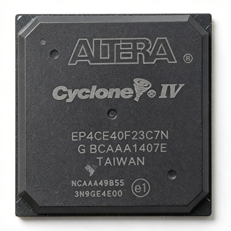
EP4CE40F23C7N - Cyclone IV E FPGA 39.6K LE 484-FBGA | Intel
The Intel (formerly Altera) EP4CE40F23C7N is a Cyclone IV E Field Programmable Gate Array (FPGA) delivering 39,600 logic elements, 1,161,216 bits of embedded memory, and 116 embedded 18x18 multipliers, all housed in a 484-ball FineLine BGA package with commercial temperature grade (0C to 85C). A Field Programmable Gate Array is a semiconductor integrated circuit built around an array of configurable logic blocks (CLBs), programmable interconnect, and dedicated hard IP blocks such as memory and DSP slices. FPGAs occupy the top of the programmable-logic hierarchy alongside CPLDs, with FPGAs typically addressing higher logic densities, on-chip memory, and high-speed serial transceivers for parallel DSP, video, and embedded processing workloads. The Cyclone IV E family is fabricated on a low-power 60 nm process and is optimized for cost-sensitive, high-volume applications. Key features of the EP4CE40F23C7N include 328 maximum user I/O pins, 4 PLLs for clock management, and 66.5 Kbits of distributed RAM. The device integrates 116 embedded multipliers for DSP workloads, supports external memory interfaces including DDR/DDR2 SDRAM and QDRII SRAM, and provides multiple configuration modes such as JTAG and Active Serial. The 484-FBGA package offers a 1.0 mm ball pitch suitable for multilayer PCB designs. The Cyclone IV E architecture combines an SRAM-based programmable fabric with hard memory blocks (M9K), DSP blocks (18x18 multipliers), and on-chip PLLs. Compared with the earlier Cyclone III family, Cyclone IV E delivers improved logic utilization, lower static power, and a richer set of I/O standards including LVDS, SSTL, and HSTL for high-speed parallel interfaces. Typical applications for the EP4CE40F23C7N include industrial motor control and factory automation, video processing and image acquisition, communications protocol bridging, software-defined radio front-ends, and embedded display controllers. The wide I/O count and embedded multipliers make it especially suitable for parallel data acquisition and DSP pipelines. When designing with this device, ensure proper decoupling with 100 nF and 10 uF capacitors near each power pin, follow Intel's recommended PCB layout guidelines for the FBGA package, and use the Quartus II design software (Cyclone IV E supported edition) for synthesis, place-and-route, and configuration bitstream generation. This page consolidates distributor pricing, drop-in alternatives from the same Cyclone IV E family, and practical design considerations that go beyond a quick datasheet lookup, helping engineers accelerate part selection and PCB bring-up.
EP4CE40F23C8 - Cyclone IV E FPGA, 39.6K LE, 484-FBGA | Intel
The Intel (formerly Altera) EP4CE40F23C8 is a member of the Cyclone IV E family of low-power, high-volume FPGAs, fabricated on a 60 nm process and packaged in a 484-ball FineLine BGA with 328 user I/O pins. The device integrates 39,600 logic elements, 1,161,216 bits of embedded memory (1134 Kbit), and 116 embedded 18x18 multipliers, making it well-suited for cost-sensitive parallel processing, motor control, video bridging, and industrial communication designs. It is built around a logic-structure of 4-input look-up tables (LUTs), true dual-port M9K memory blocks, and embedded multiplier blocks with optional pre-adder support. A Field-Programmable Gate Array (FPGA) is a semiconductor device built around an array of configurable logic blocks (CLBs), programmable interconnect, and I/O cells, all of which are customized after manufacturing via a configuration bitstream. Within the broader programmable-logic hierarchy, FPGAs sit between simple CPLDs (Complex Programmable Logic Devices) and full Application-Specific Integrated Circuits (ASICs), offering higher logic density than CPLDs and far lower NRE cost than ASICs. The Cyclone IV E family in particular targets low static and dynamic power consumption, making the architecture attractive for power-budgeted applications such as handheld test equipment and factory-floor controllers. Key features of the EP4CE40F23C8 include four general-purpose PLLs per device, support for external memory interfaces such as DDR2, DDR, LPDDR2, and QDR II SRAM, 20 global clock networks, and 66 LVDS channels (33 pairs). The configuration scheme supports Active Serial (AS), Passive Serial (PS), Fast Passive Parallel (FPP), and JTAG modes. I/O standards supported include LVTTL, LVCMOS, SSTL, HSTL, PCI, and LVDS, with per-pin dynamic on-chip termination. Operating junction temperature spans 0 C to 85 C (commercial, suffix C8). Typical applications span industrial motor-control inverters, video format converters, low-cost PCIe endpoint bridges, factory automation controllers, and low-power software-defined radio front-ends. In motor-control designs the embedded multipliers and dedicated PLLs accelerate field-oriented control (FOC) algorithms, while in display-port interface bridging the 328 user I/Os and LVDS channels provide ample bandwidth without an external transceiver. When designing with this part, allocate at least 1 sq-in of solid ground plane beneath the 484-ball FBGA and follow Intel's recommended 4-layer PCB stack-up for the impedance-controlled pairs. The configuration flash must be a 16-bit or 32-Mbit AS-mode EPCS device selected to match the cyclone IV E bitstream size. This page consolidates distributor pricing, drop-in alternatives, and practical PCB design notes not found in the manufacturer datasheet alone, giving engineers a single reference for both the electrical characterization and the supply-chain profile of the EP4CE40F23C8.
EP4CE40F23C8L - Cyclone IV E FPGA, 39.6K LEs, 484-FBGA | Intel (Altera)
The Intel (formerly Altera) EP4CE40F23C8L is a low-cost, low-power Cyclone IV E Field-Programmable Gate Array (FPGA) fabricated on a 60 nm process, delivering 39,600 logic elements, 1,161,216 bits of embedded memory, and 116 hardware multipliers in a 484-pin FineLine BGA package. It operates from a 1.2 V core supply with hot-socketing and 8 mA low-power standby support, targeting cost-sensitive high-volume applications. The device provides 328 general-purpose I/O pins and four general-purpose PLLs for clock management. What is a Cyclone IV E FPGA? A Field-Programmable Gate Array is a semiconductor device built around an array of configurable logic blocks (CLBs), programmable interconnect, and dedicated hard IP such as multipliers, memory blocks, and PLLs. Cyclone IV E sits in the low-power, low-cost tier of the Cyclone family, positioned below Cyclone V and above legacy Cyclone III devices. It belongs to the broader hierarchy of programmable logic devices (PLD), sitting alongside CPLDs in the digital logic ecosystem but offering dramatically higher logic density. The 'E' suffix designates the Enhanced logic-and-memory variant optimized for parallel processing and DSP workloads rather than high-speed serial transceivers. Key features include 4 input/output banks supporting multiple I/O standards (LVDS, LVTTL, LVCMOS, SSTL, HSTL), embedded RAM blocks up to 4 Kbits each, configurable JTAG boundary-scan, and Cyclone-specific configuration schemes including Active Serial and JTAG. The device supports up to 200 MHz internal operation in commercial temperature grades and offers configurable Multiplier blocks optimized for DSP functions. Configuration memory supports both compression and encryption for secure bitstream handling. Architecture highlights include an 8-input adaptive logic module (ALM) that improves packing efficiency over the 4-input LUT structure used in earlier Cyclone generations, a dedicated 18x18 multiplier block array, and global clock networks supported by up to 8 dedicated clock pins. The PLLs feature dynamic reconfiguration and support spread-spectrum clocking. On-chip memory totals 1.16 Mbits organized as M9K blocks of 9 Kbits each. Typical applications include industrial motor control, video processing pipelines, low-cost ASIC prototyping, embedded vision systems, and consumer electronics requiring moderate logic density without the cost of larger FPGAs. The wide temperature grade variants (denoted by the 'L' suffix) extend operation into industrial environments. Designers choose this device for parallel DSP, glue-logic consolidation, and small-to-medium state-machine implementations. Design consideration: estimate board area carefully. The 484-FBGA has 1.0 mm ball pitch and requires at least 6 PCB layers with controlled-impedance routing for high-speed I/O signals. Always reference the Cyclone IV Device Family Pin Connection Guidelines for unused-pin termination, especially for differential pairs used in LVDS modes. This page synthesizes distributor pricing, drop-in same-package alternatives, and PCB layout design notes not aggregated on any single distributor page.
EP4CE40F23C8LN - Cyclone IV E FPGA, 39.6K LE, FBGA-484 | Intel
The Intel (formerly Altera) Cyclone® IV E EP4CE40F23C8LN is a low-cost, low-power field-programmable gate array (FPGA) built on a 60 nm process, delivering 39,600 logic elements in a 484-ball fine-pitch BGA (FBGA-484) package with 1.0 mm ball pitch and 23 × 23 mm body. It features 328 maximum user I/O pins, 1,161,216 bits of embedded memory (RAM), and 116 embedded 18 × 18 multipliers, providing ample resources for parallel DSP, video bridging, and industrial control designs. A Field Programmable Gate Array (FPGA) is a reconfigurable semiconductor device whose logic fabric, routing, and I/O can be programmed in the field to implement arbitrary digital circuits, sitting architecturally between fixed-function ASICs and software-driven microcontrollers in the broader semiconductor hierarchy: FPGA → programmable logic → digital IC → semiconductor. Cyclone IV E devices specifically target cost- and power-sensitive applications where designers need ASIC-like integration without the NRE cost of custom silicon. Key features of this device include four general-purpose PLLs per device, 20 global clock networks, support for external memory interfaces such as DDR/DDR2/QDR II SRAM, and the C8 speed grade with industrial temperature rating (suffix "I" would be explicitly industrial; this part uses the C8L designation). The "8" suffix denotes the 8 ns speed grade internal timing, while the "L" indicates lead-free / Pb-free packaging compliant with RoHS. The die operates from a 1.2 V core supply with separate 1.2 V / 2.5 V / 3.3 V I/O bank supplies, enabling mixed-voltage interfacing without external level shifters. The EP4CE40F23C8LN is widely used in industrial automation, motor control, video processing, communications infrastructure, and ASIC prototyping where mid-range logic density (39.6K LE) is required. Its high multiplier count and ample block RAM make it particularly suitable for DSP pipelines and multi-channel data acquisition. Designers benefit from the Quartus Prime design suite support, including the free Quartus Prime Lite edition, which covers the full Cyclone IV E family. When designing with this part, ensure the FBGA-484 PCB footprint meets the 1.0 mm ball pitch with non-solder-mask-defined (NSMD) pads per IPC-7351, and provide sufficient via-in-pad or dog-bone fanout for signal escape routing. Thermal management is generally passive at typical industrial operating points, but junction temperature must be verified against the application power profile using the Quartus PowerPlay estimator. This page synthesizes distributor pricing, drop-in alternative OPNs within the same FBGA-484 footprint, and practical design notes not found in the manufacturer datasheet alone.
EP4CE40F23C8N - Cyclone IV E FPGA, 39.6K LE, 484-FBGA | Intel
The Intel (formerly Altera) EP4CE40F23C8N is a Cyclone IV E family Field Programmable Gate Array (FPGA) integrating 39,600 logic elements, 1,134 Kbit embedded memory, and 328 user I/Os in a 484-ball FineLine BGA (FBGA) package. Built on a low-power 60 nm process, it targets cost-sensitive, high-volume applications requiring a balance of logic density, memory bandwidth, and I/O flexibility without transceivers. An FPGA (Field Programmable Gate Array) is a programmable logic device whose interconnect and function blocks can be configured after manufacture by loading a bitstream into SRAM-based configuration memory. Within the broader semiconductor taxonomy, FPGAs sit above CPLDs (Complex Programmable Logic Devices) in logic capacity and below ASICs in per-unit cost. The Cyclone IV E sub-family belongs to the low-cost, non-transceiver branch of the Cyclone IV family, sharing the same Quartus Prime design environment as Cyclone IV GX parts. Key features include 4 PLLs for clock synthesis, 66 embedded 18x18 multipliers supporting DSP operations up to ~150 MHz, 1161 Kbit of M9K block RAM, and support for external memory interfaces such as DDR, DDR2, and QDR II SRAM. User I/O voltages are programmable to 1.2 V, 1.5 V, 1.8 V, 2.5 V, 3.3 V, and LVDS, and the device operates from a 1.2 V core supply with a separate PLL analog supply. The 484-ball FBGA package provides a 1.0 mm ball pitch suitable for multilayer PCB fabrication with standard reflow profiles. Configuration options include JTAG, Active Serial (AS), and Passive Serial (PS) modes using a serial flash or download cable. Typical applications include industrial motor control, video processing bridges, LED display controllers, and PCIe endpoint soft IP implementations on the Cyclone IV E family. The part is also well-suited for prototyping ASIC functionality, machine vision preprocessing, and protocol bridging between legacy and modern interfaces. When designing with this part, ensure the PCB supports the 1.0 mm BGA pitch with microvia or via-in-pad fabrication, and provision decoupling close to each bank supply. Configuration mode selection at MSEL pins must match the selected boot source, otherwise the device will fail to configure. This page synthesizes Cyclone IV E specifications, drop-in alternatives with the same FBGA-484 footprint, and practical design notes not consolidated in the manufacturer datasheet.
EP4CE40F23C8N7N - Cyclone IV E FPGA 39.6K LE | Altera | 484-FBGA
The Altera EP4CE40F23C8N7N is a Cyclone IV E family Field-Programmable Gate Array (FPGA) built on a 60 nm low-power process, integrating 39,600 logic elements (LEs), 1,161,216 bits of embedded memory, and 328 user I/O pins into a 484-ball FineLine BGA (FBGA) package. It supports a core voltage of 1.2 V with I/O bank voltages configurable between 1.2 V and 3.3 V, enabling direct interface to DDR2/DDR3, LVDS, LPDDR2, and legacy LVCMOS/LVTTL logic without external level shifters. The device is rated speed grade 8 (C8) at commercial temperature and ships in Pb-free, RoHS-compliant packaging. An FPGA (Field-Programmable Gate Array) is a reconfigurable integrated circuit containing an array of programmable logic blocks, configurable interconnect, embedded memory blocks, DSP blocks, and hardened I/O peripherals. Unlike an ASIC, the logic function of an FPGA is defined after manufacture by loading a configuration bitstream into on-chip SRAM. Within the broader semiconductor taxonomy, an FPGA is a programmable logic device -> logic IC -> integrated circuit. The Cyclone IV E family is positioned as a low-cost, low-power FPGA, ideally suited to high-volume, cost-sensitive applications such as industrial motor control, video bridging, and I/O expansion. The EP4CE40F23C8N7N provides up to 4 PLLs, 116 embedded 18x18 multipliers (DSP blocks), and 66 embedded M9K memory blocks. Configuration is supported through JTAG (IEEE 1149.1), Active Serial (AS), and Passive Serial (PS) modes via a dedicated 8-pin AS interface. The device supports Cyclone IV I/O features including programmable drive strength, slew rate control, bus-hold, and 3.3 V tolerance on all I/O pins, simplifying board-level design when interfacing to legacy peripherals. Typical applications include industrial machine vision and barcode scanners, video surveillance and display controllers, motor drive and encoder interfaces, automotive infotainment preprocessing, and low-cost PCIe protocol endpoints via external PHY. The Cyclone IV E family is widely used in volume production designs where higher-end Cyclone IV GX/GT or Cyclone V devices are unnecessary. When designing with the EP4CE40F23C8N7N, ensure all I/O banks are powered before configuration to avoid I/O latch-up. Use the Altera Quartus II / Quartus Prime design environment (latest supported version) for synthesis, place-and-route, and timing closure. Decouple every VCCINT, VCCA, VCCIO, and PLL power pin with 100 nF + 10 uF caps placed within 5 mm of each ball.
EP4CE40F23C9L - Cyclone IV E FPGA 39.6K LE | Intel
The Intel EP4CE40F23C9L is a member of the Cyclone IV E FPGA family, delivering 39,600 logic elements and 113.4 Mbits of embedded memory in a 484-ball FineLine BGA package. Manufactured on a 60 nm low-power process, this device operates from a 1.2 V core supply with multi-voltage I/O support, and is offered in a commercial temperature grade with Pb-free / lead-free termination finish. A Field Programmable Gate Array (FPGA) is a reprogrammable semiconductor device that allows engineers to implement arbitrary digital logic, ranging from glue logic and state machines to complex pipelines and soft processors, by configuring an array of programmable logic elements and interconnect. Within the broader semiconductor taxonomy, FPGAs sit under programmable logic devices (PLD), which in turn fall under digital logic ICs and ultimately integrated circuits. The Cyclone IV E family specifically targets cost-sensitive, high-volume, low-power applications where the flexibility of an FPGA is required but the absolute performance of a high-end Stratix class device is not needed. Key features of the EP4CE40F23C9L include up to 396 user I/Os, 4 PLLs for clock synthesis and management, dedicated hardware multipliers, embedded configuration memory, and the ability to be reconfigured in-system through JTAG or active serial interfaces. The 484-ball FBGA package measures 23 x 23 mm with a 1 mm ball pitch and a substrate height profile suitable for high-density PCB layouts. The device supports DDR/DDR2/QDR/DDR3 external memory interfaces and integrates advanced I/O features such as LVDS, RSDS, mini-LVDS, and SSTL signaling. Architecturally, the Cyclone IV E family uses an SRAM-based LUT-driven fabric, which means the configuration bitstream must be loaded at power-up from external flash or a configuration controller. The EP4CE40F23C9L is offered in the 'C9' speed grade, which is the slowest (most economical) device grade in the Cyclone IV E family; faster speed grades (C8, C7, C6) provide higher Fmax at higher cost. The device supports hot-socketing and PCI Express hard IP blocks, simplifying interface implementation for embedded designs. Typical applications include industrial control systems, video processing and image processing front-ends, telecommunications line cards, motor control, test and measurement instrumentation, and low-cost prototyping of ASIC designs. The wide temperature support and abundant logic resources make it a popular choice for mid-volume embedded designs where NRE cost must be minimized. When designing with this FPGA, ensure that the Quartus II / Quartus Prime toolchain version supports the Cyclone IV E device family, verify that the PCB layout provides sufficient decoupling near each power pin, and confirm the configuration scheme (AS, PS, JTAG) and clock topology are consistent with the rest of the system.
EP4CE40F23C9LN - 39,600-Cell FPGA | Intel | Embedded Logic
Intel EP4CE40F23C9LN is a Cyclone IV E field-programmable gate array containing 39,600 cells and 2,475 configurable logic blocks in a 484-ball, 23 mm by 23 mm FBGA package. Verified sources identify 328 user I/Os, a 1 mm ball pitch, a 265 MHz listed frequency, and a 472 MHz internal-frequency specification. The device targets cost-sensitive embedded logic, digital interfacing, control, and signal-processing systems where reconfigurable hardware is required without the power or cost of a larger FPGA. A field-programmable gate array, or FPGA, is a semiconductor device built from programmable logic elements, routing resources, input/output blocks, and embedded functional blocks. Its configuration can be changed after circuit-board assembly. Within the system hierarchy, the FPGA sits between fixed-function processors and custom integrated circuits: it offers more deterministic parallel processing than a general-purpose processor while avoiding the high nonrecurring engineering cost of an application-specific integrated circuit. The principal capacity figures are 39,600 logic cells and 2,475 CLBs, supported by 328 I/Os in the 484-ball package. The supplied data also reports 1,161,216 bits, a 23 mm by 23 mm body, and 1 mm pitch. These attributes make the device suitable for bridges, state-machine implementations, instrument control, industrial automation, and moderate-density digital processing. Configuration storage, embedded blocks, and supported I/O standards must be confirmed in the complete manufacturer datasheet before release to production. Cyclone IV E devices are offered with 1.0 V or 1.2 V core-voltage variants, according to the manufacturer-family material provided. The C9 ordering designation and the F23 package code identify the commercial-speed, 484-ball implementation. The distinction between the 265 MHz listed frequency and 472 MHz internal-frequency entry should be resolved against the applicable timing tables and operating conditions rather than treated as one interchangeable performance rating. Typical uses include industrial controllers, communications-interface aggregation, test equipment, image preprocessing, motor-control sequencing, and educational or prototyping platforms. The 328 available I/Os are useful when many parallel sensors, converters, memories, or control peripherals must be connected. Firmware-like FPGA configuration data, power sequencing, decoupling, clock integrity, and pin-compatible substitution must be evaluated as part of system validation. Designers should preserve the exact 484-ball FBGA land pattern, validate all bank-specific I/O voltages, and confirm timing with the intended speed grade and configuration mode. A search result describing EP4CE6E22C8 does not establish package or pin compatibility; it should not be used as a drop-in substitute without complete pinout and parametric verification. This page combines the verified distributor specifications, official ordering-part information, same-family ordering options, explicit data-needed markers, and a drop-in analysis that requires package, pinout, and parameter evidence. It is intended to reduce sourcing ambiguity while keeping unverified electrical, thermal, lifecycle, compliance, and supply claims separate from confirmed values.
EP4CE40F23I7 - 39.6K Logic Elements, 484-FBGA Cyclone IV FPGA | Intel
The Intel (formerly Altera) EP4CE40F23I7 is a Cyclone IV E family field-programmable gate array (FPGA) with 39,600 logic elements, 2,475 logic array blocks, and 328 maximum user I/O pins, housed in a 484-ball fine-pitch BGA (FBGA-484, 23x23 mm, 1.0 mm pitch) package. The device operates at a maximum internal frequency of approximately 472.5 MHz from a 1.2 V core supply and is specified for the industrial temperature range of -40C to +100C. An FPGA (Field-Programmable Gate Array) is a type of programmable logic device (PLD) that sits in the broader semiconductor hierarchy as a digital IC. Unlike an ASIC, an FPGA's logic fabric is configured after manufacturing via SRAM-based configuration memory. FPGAs integrate programmable logic elements, configurable interconnect, dedicated hardware blocks (DSP, BRAM, PLLs), and I/O serdes into a single die, occupying the role of a hardware accelerator, glue-logic aggregator, and rapid-prototyping platform in modern digital systems. Key features of the EP4CE40F23I7 include 113,560 total RAM bits distributed across M9K blocks, 116 embedded 18x18 multipliers for DSP workloads, four general-purpose PLLs for clock synthesis, and support for LVDS, LVTTL, LVCMOS, SSTL, and HSTL I/O standards. The device is fabricated on a low-power 60 nm process that delivers an attractive performance-per-watt envelope versus earlier Cyclone generations. Architecturally, the Cyclone IV E family uses a logic-element (LE) based fabric where each LE contains a 4-input LUT, a programmable register, and carry-chain logic. Distributed M9K memory blocks (9 Kbit each) provide on-chip data storage for FIFOs, buffers, and shift registers, while 18x18 multipliers enable single-cycle DSP operations. The four PLLs support dynamic phase shifting and reconfigurable clock synthesis, and the periphery contains LVDS-capable I/O pairs for high-speed source-synchronous interfaces. Typical applications for the EP4CE40F23I7 span industrial motor control and factory automation, video processing and broadcast equipment, telecom line cards, automotive driver-assistance prototypes, medical imaging, and cost-sensitive ASIC replacement in mid-volume designs. The combination of logic density, on-chip memory, and DSP blocks positions this device as a versatile mid-density platform. Designers should plan PCB layout to the 1.0 mm BGA pitch, route at least four layers with a solid ground plane under the package, and provide clean 1.2 V/2.5 V/3.3 V rails with bulk decoupling adjacent to the device. Quartus Prime or Quartus II software is required for synthesis, place-and-route, and bitstream generation; JTAG or Active Serial configuration memory loads the SRAM-based configuration on power-up. This page synthesizes distributor pricing, drop-in alternative SKUs, and practical PCB/design guidance not found in the bare manufacturer datasheet - giving component buyers, hardware engineers, and FPGA developers a single decision-ready reference.
EP4CE40F23I7N - Cyclone IV E FPGA 39.6K LE 484-BGA | Intel
The Intel (Altera) EP4CE40F23I7N is a low-power, low-cost Cyclone IV E Field Programmable Gate Array (FPGA) with 39,600 logic elements, 1,161,216 bits of embedded memory, and 328 maximum user I/Os, housed in a 484-pin FineLine BGA (FBGA-484) package at industrial temperature grade. The device integrates 116 hardware multipliers (18x18) and four general-purpose PLLs, supporting internal clock rates up to approximately 472 MHz, and operates from a 1.0 V core / 1.2 V / 2.5 V / 3.3 V selectable bank voltage scheme typical of the Cyclone IV E family. A Field Programmable Gate Array (FPGA) is a programmable semiconductor device whose logic, interconnect, and I/O behavior are defined after manufacture by a user-supplied configuration bitstream. FPGAs sit in the broader taxonomy of programmable logic devices (PLDs) -> programmable logic -> digital semiconductors. Cyclone IV E is a cost-optimized SRAM-based FPGA family targeting high-volume applications where ASIC non-recurring engineering cost is prohibitive but fixed function ASICs are too rigid. Key differentiating features of this part include: 39,600 logic elements, 4 PLLs with up to 472 MHz operation, 1,161,216 bits of embedded RAM organized into M9K blocks, 116 embedded 18x18 multipliers supporting DSP functions, and 328 user I/Os across eight I/O banks supporting multiple I/O standards (LVDS, LVCMOS, SSTL, HSTL). The device is built on a 60 nm low-power process and includes configuration support via Active Serial (AS), Passive Serial (PS), and JTAG modes. Architecturally, Cyclone IV E FPGAs use a logic-element fabric with 4-input look-up tables, dedicated carry chains, and tightly coupled M9K memory blocks. The 18x18 multipliers support up to 250 MHz DSP throughput without consuming general logic resources. Configuration memory is SRAM-based, requiring an external configuration flash or EPCS device for standalone boot. The device is pin-compatible within the same package option across speed grades and temperature grades, simplifying board-level migration. Typical applications include industrial motor control and machine vision, video processing and display bridges, automotive infotainment subsystems, low-cost ASIC prototyping, communications protocol bridging, and embedded digital signal processing (DSP) pipelines. The combination of high logic count, embedded multipliers, and low unit cost makes Cyclone IV E a frequent choice for volume production where mid-range FPGA capacity is sufficient. When designing with this device, allocate at least 25 percent of the FPGA's logic for routing overhead, and verify that the JTAG chain ordering matches the PCB layout. Plan configuration flash capacity carefully - an EP4CE40 bitstream typically requires roughly 10 Mbits of configuration memory. Thermal management is generally not required for industrial applications because the 60 nm process keeps total power dissipation well below 5 W for typical designs. This page synthesizes distributor pricing, drop-in alternatives drawn from the same Altera/Intel Cyclone IV E family, and practical design notes not found in the manufacturer datasheet alone.
EP4CE40F23I8L - Cyclone IV E FPGA, 39.6K LE, 484-BGA | Intel
The Intel EP4CE40F23I8L is a Cyclone IV E field-programmable gate array (FPGA) built on a 60 nm low-power process, integrating 39,600 logic elements (LEs), 1,161,216 bits of embedded memory, and 328 maximum user I/Os in a 484-ball FineLine BGA (FBGA-484) package. It supports a core voltage of 1.0 V (0.97 V to 1.03 V) and is offered in the -I8L industrial speed grade with extended temperature range. The part provides 4 PLLs, 113 embedded 18x18 multipliers, and up to 532 Kbits of M9K memory blocks. What is a Cyclone IV E FPGA? It is a low-cost, low-power SRAM-based programmable logic family from Intel (formerly Altera) that targets volume-driven applications such as industrial control, video processing, and communications bridging. Cyclone IV E sits in the FPGA hierarchy below high-performance Stratix families and above legacy Cyclone III devices, optimized for low static and dynamic power while preserving abundant DSP, memory, and I/O resources for cost-sensitive designs. Key features include 2,475 logic array blocks (LABs) and 113 DSP blocks, 4 general-purpose PLLs with fractional output capability, and 8 user I/O banks supporting a wide range of single-ended and differential I/O standards including LVDS, SSTL, and HSTL. Hard memory controller support for DDR/DDR2/DDR3 SDRAM and LPDDR2 simplifies external memory interfaces. Each Cyclone IV E device embeds a Configuration via EPCS or JTAG, and supports single-event upset (SEU) mitigation through Cyclone IV's CRC and scrubber IP. Architecturally, the EP4CE40F23I8L uses a 4-input look-up table (LUT) fabric, distributed M9K memory blocks (each 9 Kbits), and dedicated 18x18 multipliers connected through a multi-track interconnect. The I8L speed grade combined with industrial temperature range makes it suitable for outdoor and harsh-environment deployments. Typical applications include industrial motor control and PLCs, video surveillance and image processing, software-defined radio front-ends, low-cost ASIC prototyping, and PCIe endpoint bridges using external PHY. Designers also choose Cyclone IV E for display controllers, sensor aggregation, and general glue-logic replacement. Designers should budget power by leveraging Intel's PowerPlay tools and the Early Power Estimator (EPE) spreadsheet, since logic utilization and toggle rate dominate dynamic power. For high-speed LVDS or DDR3 interfaces, follow the Cyclone IV External Memory Interface Guidelines and match length within 50 mils on byte lanes. This page consolidates verified distributor pricing, drop-in same-footprint alternatives, and practical design notes not found in the manufacturer datasheet alone.
EP4CE40F23I8LN - 39.6K LE Cyclone IV E FPGA, 484-FBGA | Intel
The Intel (formerly Altera) EP4CE40F23I8LN is a low-cost, low-power Cyclone IV E field-programmable gate array (FPGA) integrating 39,600 logic elements, 1,161,216 bits of embedded memory, and 328 maximum user I/Os in a 484-ball fine-pitch BGA (FBGA-484) package built on a 60 nm process node. The device operates from a 1.2 V core supply, supports up to four PLLs, and provides 132 embedded 18x18 multipliers for DSP-style arithmetic. The industrial temperature grade "I8" supports -40C to +85C ambient operation. A Cyclone IV E FPGA is a SRAM-based programmable logic device that combines configurable logic blocks, embedded memory arrays, DSP blocks, and high-speed I/O into a single chip. It belongs to the broader taxonomy FPGA -> programmable logic -> logic IC -> integrated circuit -> semiconductor, and targets cost-sensitive high-volume designs where ASSPs and ASICs are uneconomical. The Cyclone IV E family is optimized for low static and dynamic power, making it well suited to fan-less, thermally constrained embedded systems. Key features include 39,600 logic elements organized into 2,475 logic array blocks, 1,161,216 bits of embedded SRAM (RAM), 4 PLLs for clock synthesis, embedded multipliers supporting DSP, and 8 clock networks. The device supports LVDS, LVTTL, LVCMOS, SSTL, and RSDS I/O standards and offers configuration via JTAG, Active Serial, or Passive Serial modes. Architecturally, the EP4CE40F23I8LN uses a four-input look-up table (LUT) logic element paired with a dedicated carry chain and an adjacent programmable register. Embedded memory blocks are 9 Kbit M9K blocks, with each capable of true dual-port operation. DSP blocks implement 18x18 signed multiplication with optional addition/subtraction/accumulation. Configuration data is stored in an internal SRAM that is loaded at power-up from an external flash device or the JTAG port. Typical applications include industrial motor control and factory automation, video processing and display bridging, telecom line cards, software-defined radio front-ends, automotive infotainment prototypes, and education kits. Cyclone IV E devices are commonly paired with EPCS serial configuration memories and DDR/DDR2 SDRAM controllers implemented in the FPGA fabric. Design considerations include PCB routing for the 1 mm pitch FBGA, multi-rail decoupling (1.2 V core, 2.5 V/3.3 V I/O, PLL analog), and proper configuration mode pin strapping. Designers should follow the Intel Cyclone IV device handbook for pin connection guidelines, especially for nCONFIG, nSTATUS, and CONF_DONE pins. This page combines distributor pricing, same-brand drop-in alternatives from the Cyclone IV E family, and practical design notes not found in the manufacturer datasheet alone.
EP4CE40F29C6 - 39.6K LE Cyclone IV E FPGA, 532 I/O, 780-BGA | Altera
The Altera (Intel) EP4CE40F29C6 is a Cyclone IV E family Field Programmable Gate Array (FPGA) fabricated on a 60 nm process, delivering 39,600 logic elements, 1,161,216 bits of embedded memory, and 532 user I/O pins in a 780-ball FineLine BGA (FBGA) package. The device integrates 116 hardware multipliers (18x18) for DSP-centric functions and supports core voltages of 1.2 V with commercial 0C to +85C operating temperature grading. The 780-BGA package offers high I/O density for pin-rich designs in industrial control, video processing, and embedded computing. What is an FPGA? A Field-Programmable Gate Array is a semiconductor integrated circuit built around an array of configurable logic blocks (CLBs), programmable interconnect, and dedicated hard-IP blocks such as memory, multipliers, transceivers, and PLLs. FPGAs sit in the broader taxonomy of programmable logic devices (PLDs), above CPLDs (which are simpler, non-volatile), and below ASICs (custom-fabricated). The Cyclone IV E series specifically targets cost-sensitive, high-volume applications by balancing logic density, memory, and DSP against low unit cost and low static power consumption, sitting in Altera/Intel's product hierarchy below Cyclone V and Stratix families. Key features of the EP4CE40F29C6 include 4 PLLs for clock management, support for LVDS, LVCMOS, SSTL, and HSTL I/O standards, and a built-in configuration controller supporting JTAG (IEEE 1149.1) and Active Serial (AS) modes. The device offers up to 4 Mb of embedded SRAM distributed across M9K blocks (typically 113 blocks at 9 Kbit each), enabling efficient buffer and FIFO implementation without consuming logic resources. The 780-BGA package provides high signal density for memory-intensive designs and parallel interface bridging. The EP4CE40F29C6 architecture uses 4-input lookup tables (LUTs) and embedded multiplier blocks optimized for parallel arithmetic. Its 60 nm process node minimizes leakage while supporting clock rates in the 200-400 MHz range for typical logic paths. Multiple I/O banks allow mixed-voltage interfacing (1.2 V to 3.3 V), and the configuration memory is SRAM-based, requiring an external flash or configuration controller for volatile designs. Typical applications include industrial motor control and machine vision, video surveillance systems, automotive infotainment, LED video walls, software-defined radio, embedded prototyping, and high-volume consumer electronics. The 532 user I/Os make it well-suited for parallel data acquisition, memory expansion, and bus bridging applications. When designing with this device, ensure the PCB has adequate BGA escape routing (microvia or via-in-pad recommended for inner balls), power decoupling per Cyclone IV guidelines, and a configuration scheme selected (JTAG for development, AS flash for production). Thermal management should account for the commercial temperature grade of 0C to +85C, ensuring junction temperature remains within datasheet limits. This page synthesizes distributor pricing, same-family drop-in alternatives, and practical design notes not consolidated on the manufacturer datasheet, enabling faster design-in and sourcing decisions.
EP4CE40F29C6N - Cyclone IV E FPGA 39.6K LE | Intel | 780-BGA
The Intel (formerly Altera) EP4CE40F29C6N is a Cyclone IV E Field Programmable Gate Array (FPGA) with 39,600 logic elements, 1,161,216 bits of embedded memory, and 532 user I/Os, packaged in a 780-ball FineLine BGA (F29) at commercial 0°C–85°C temperature grade with speed grade 6. It is a member of the low-cost, low-power Cyclone IV E family built on a 60 nm process. What is an FPGA? A Field Programmable Gate Array is a digital semiconductor containing an array of configurable logic blocks (CLBs), programmable interconnect, and dedicated hard IP such as memory blocks, DSP blocks, PLLs, and SERDES. FPGAs sit in the programmable-logic tier of the broader digital-semiconductor hierarchy: ASIC < FPGA < programmable SoC < microprocessor. The Cyclone IV E family was engineered for cost-sensitive, high-volume applications that previously used ASICs or CPLDs. Key features of the EP4CE40F29C6N include 39,600 logic elements arranged into 4-input adaptive logic modules (ALMs), 4 M9K embedded memory blocks (113 blocks total) totaling 1,161,216 RAM bits, 66 18x18 hardware multipliers, four general-purpose PLLs, and 532 maximum user I/Os. The 780-BGA (F29) package provides the highest I/O count and largest pin pitch of the EP4CE40 family, suitable for high-density board designs. Architecturally, the Cyclone IV E device uses a 1.2 V core supplied by an on-die linear regulator. Configuration is via serial (AS) flash, JTAG, or passive serial. Static power consumption is among the lowest in its class, and the device supports hot-socketing and octal configuration modes. The 60 nm TSMC process allows operation down to 1.0 V core with internal regulation. Typical applications include industrial motor control and machine vision, automotive infotainment prototypes, video processing and display controllers, communications line cards, software-defined radio front-ends, and ASIC prototyping. The wide logic and DSP capacity also make it useful for embedded data acquisition and DSP co-processing. Designers should plan FPGA power sequencing with the 1.2 V core supply ramped first and the I/O banks following, follow Altera's recommended decoupling scheme, and use the Quartus II/Prime toolchain for place-and-route. This page consolidates Cyclone IV E pricing, drop-in FPGA alternatives, and design notes that complement the official datasheet.
EP4CE40F29C7 - Cyclone IV E FPGA, 39.6K LE, 780-FBGA | Intel
Intel EP4CE40F29C7 is a Cyclone IV E family field-programmable gate array (FPGA) built on a 60 nm low-power process, integrating 39,600 logic elements, 1,161,216 bits of embedded memory, and 532 user I/O pins in a 780-ball fine-pitch BGA (FBGA) package. Core voltage is 1.2 V with multi-voltage I/O support. A Field-Programmable Gate Array (FPGA) is a semiconductor integrated circuit that can be reconfigured by the customer after manufacture to implement arbitrary digital logic, DSP blocks, and memory functions. FPGAs sit hierarchically between fixed-function ASICs and software-programmable processors, combining hardware-level parallelism with software-like design iteration. The Cyclone IV E family specifically targets cost-sensitive, high-volume applications where low static power (sub-1.5 W typical) and high I/O density matter more than the highest possible logic throughput. Key differentiating specifications include 4 embedded PLLs for clock synthesis, up to 113 embedded 18x18 multipliers for DSP, dedicated hardware for DDR/DDR2/QDR II memory interfaces, and support for LVDS, LVPECL, SSTL, and HSTL I/O standards. The device supports both asynchronous and synchronous external memory and includes configuration support via passive serial, active serial, and JTAG modes. Architecturally, the EP4CE40F29C7 uses look-up-table (LUT) based logic blocks grouped into Logic Array Blocks (LABs), each containing 16 logic elements. Embedded memory is implemented as true dual-port M9K blocks, while DSP operations are accelerated by dedicated multiplier blocks, freeing fabric logic for control and routing. Hard PCIe, PLL, and memory controller silicon blocks reduce soft logic overhead and improve timing closure. Typical applications include industrial motor control, video processing bridges, low-cost software-defined radio front-ends, telecom line cards, and embedded vision prototypes. The wide I/O count and DSP density also suit automotive infotainment pre-production boards and aerospace test instrumentation. When designing with this FPGA, plan power sequencing for 1.2 V core before 2.5/3.3 V I/O, allocate sufficient decoupling (100 nF + 10 µF per supply rail), and verify JTAG chain integrity before attempting configuration. Quartus II design software (Cyclone IV device support) is required for synthesis, place-and-route, and bitstream generation. This page synthesizes distributor pricing from DigiKey, Mouser, and Heisener, alongside drop-in same-family alternatives and engineering design notes not aggregated in any single manufacturer datasheet, providing a unique cross-reference for engineers evaluating this Cyclone IV E variant.
EP4CE40F29C7N - Cyclone IV E FPGA, 40K LE, 780-FBGA | Intel / Altera
The Intel (formerly Altera) EP4CE40F29C7N is a Cyclone® IV E family Field Programmable Gate Array (FPGA) with 39,600 logic elements, 1,161,216 bits of embedded memory, and 532 hardware multipliers (18x18), housed in a 780-ball FineLine BGA (FBGA) package with commercial temperature grade (0°C to +85°C) and -7 speed grade. Built on a 60 nm low-power process and operating from a 1.2 V core supply, it integrates programmable logic, embedded memory blocks, DSP blocks, and PLLs on a single die optimized for cost-sensitive high-volume applications. What is an FPGA? An FPGA (Field Programmable Gate Array) is a semiconductor device whose digital logic function is defined after manufacturing by the user, rather than at the foundry. The device contains an array of configurable logic blocks (CLBs), programmable routing, embedded memory (BRAM), DSP blocks, and high-speed I/O and transceiver channels. FPGAs sit above microcontrollers in flexibility and below ASICs in unit cost, occupying the role of programmable hardware accelerator in the broader taxonomy: programmable logic device -> FPGA -> SRAM-based FPGA -> low-cost FPGA family. Key features of the EP4CE40F29C7N include 4 PLLs, up to 532 user I/O pins routed through 8 I/O banks, support for external memory interfaces such as DDR/DDR2 SDRAM and QDRII SRAM, and Cyclone IV E's signature low static and dynamic power. The -7 speed grade places this device in the middle of the Cyclone IV E speed range, with internal clock frequencies reaching approximately 400-500 MHz depending on the design. Architecturally, the Cyclone IV E family uses a 4-input LUT-based logic element, true-dual-port M9K memory blocks, and 18x18 signed multipliers that can be cascaded into larger DSP structures. The on-chip configuration controller supports both active serial (AS) and JTAG programming modes. The 780-FBGA package exposes the full I/O count of this die variant, enabling connectivity to high-bandwidth parallel buses, memory channels, and LVDS links. Typical applications include industrial motor control and machine vision, video processing and broadcast equipment, telecommunications line cards, USB and PCIe bridging (using external PHYs), automotive infotainment prototypes, and cost-optimized ASIC prototyping. The combination of mid-range logic density, embedded multipliers, and rich memory makes the EP4CE40 well-suited for DSP-heavy designs such as software-defined radio front-ends and baseband signal processing. When designing with this device, ensure the Quartus Prime toolchain is matched to the silicon revision, plan decoupling across all VCCINT, VCCA, and VCCIO rails, and verify pinout against the IBIS model for signal-integrity-critical I/O standards. The 780-FBGA package requires an ENIG or ENEPIG surface finish and careful via-in-pad microvia stack design. This page synthesizes distributor pricing, drop-in same-family alternatives, and practical Quartus design notes that go beyond the Cyclone IV E Device Handbook to help engineers shorten the BOM selection and PCB bring-up cycle.
EP4CE40F29C8 - 39.6K LE Cyclone IV E FPGA, 780-FBGA | Intel
The Intel (formerly Altera) EP4CE40F29C8 is a Cyclone IV E family Field Programmable Gate Array (FPGA) built on a low-power 60 nm process, delivering 39,600 logic elements, 1,161,216 bits of embedded memory, and 532 user I/O pins in a 780-ball FineLine BGA (FBGA) package. Per the DigiKey product listing, it operates as a logic density upgrade over the EP4CE30 while retaining the same F29 package pinout, enabling direct PCB-level swaps where higher LUT count is needed. Speed grade C8 places it in the mid-tier of the Cyclone IV E speed bin, and the commercial temperature grade (0C to +85C) covers most indoor industrial and embedded use cases. A Field Programmable Gate Array (FPGA) is a semiconductor device containing an array of configurable logic blocks (CLBs), programmable interconnect, and dedicated hardware such as block RAM, DSP blocks, and PLL/clock trees, all of which can be rewired post-manufacture to implement arbitrary digital circuits. Cyclone IV E sits at the low-end of Intel's FPGA portfolio, positioned as the most cost-optimized SRAM-based FPGA family for high-volume applications such as industrial control, video bridging, motor drive, and I/O expansion. Compared with its predecessor Cyclone III, Cyclone IV E halves the core power consumption while preserving the same Quartus II / Quartus Prime design flow. Key features of the EP4CE40F29C8 include 4 PLLs for clock synthesis and skew management, 116 embedded 9x9 multipliers for moderate DSP workloads, up to 8 configuration schemes supported through the dedicated configuration pins, and built-in PCI Express hard IP block (PIPE) on certain Cyclone IV E variants. The 780-FBGA package exposes the full I/O count of the device, allowing designers to maximize external connectivity without resorting to a larger device. Technically, the device is powered from a 1.2 V core rail with separate VCCIO banks for flexible I/O standard support (LVDS, SSTL, HSTL, LVCMOS up to 3.3 V). Configuration can be loaded via JTAG, passive serial, or active serial flash, and the device supports remote upgrade via the dual-image configuration feature. Embedded block RAM totals 270 kbit (M9K blocks) with true dual-port operation, and the four PLLs support independent frequency synthesis with reconfigurable bandwidth. Typical applications for the EP4CE40F29C8 span industrial motor control drives, LED video walls and display controllers, machine vision pre-processing pipelines, automotive infotainment head units, and PCIe Gen1 endpoint cards. The combination of mid-range logic density, low static power, and rich I/O makes it particularly attractive for I/O aggregation bridges that previously required a CPLD plus a microcontroller. When designing with this device, plan thermal dissipation for the FBGA package early - although core power is modest, dense I/O switching on 532 pins can drive junction temperature rise. Use the Quartus Prime PowerPlay Power Analyzer to estimate worst-case power before committing to a layout that lacks thermal vias under the BGA. This page synthesizes distributor pricing, verified drop-in alternatives within the same Cyclone IV E family, and practical design notes not collated in the manufacturer datasheet.