FPGA & CPLD
Products (6352)
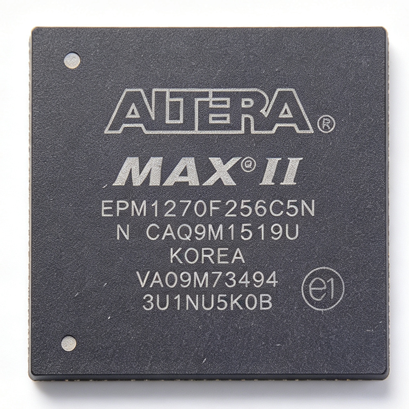
EPM1270F256 - MAX II 980-Macrocell CPLD, 256-BGA | Altera
The Altera (Intel PSG) EPM1270F256 is a member of the MAX II family of instant-on, non-volatile CPLDs, offering 980 typical equivalent macrocells (1270 LEs) in a 256-pin FineLine BGA package. According to the manufacturer datasheet, the device is built on a 0.18 µm process, operates from a 2.5 V / 3.3 V core supply, and supports user I/O up to 212 pins with a system frequency up to 201.1 MHz. It uses a non-volatile flash configuration cell that delivers instant-on functionality and eliminates external boot memory, simplifying board design in glue-logic and bus-interface applications. A CPLD (Complex Programmable Logic Device) is a non-volatile programmable logic device that combines the architectural simplicity, deterministic timing, and instant-on behavior of classic PAL/GAL logic with modern high-pin-count integration. Within the broader programmable-logic taxonomy, the MAX II family sits between simple 5-V SPLDs and high-density SRAM-based FPGAs: like SPLDs it is non-volatile and pin-configurable, but like an FPGA it integrates thousands of gates and dozens of I/O standards. MAX II devices are widely used as interface bridges, I/O expanders, and timing controllers in cost-sensitive industrial and consumer systems. Key features of the EPM1270F256 include 980 macrocells / 1270 logic elements, 8 Kbits of user flash memory, on-chip voltage regulators supporting 3.3 V, 2.5 V, 1.8 V, and 1.5 V operation, MultiVolt core and I/O supporting mixed-voltage interfacing, JTAG (IEEE 1149.1) boundary-scan programming, and an instant-on configuration time measured in microseconds. The 256-pin FineLine BGA footprint provides flexible I/O bank placement while preserving vertical migration to the EPM570 and EPM2210 in the same package. Architecturally, the EPM1270F256 implements the Logic Array Block (LAB) structure with 16 macrocells per LAB, a fast t<sub>PD</sub> in the single-digit nanosecond range, and a deterministic interconnect that makes it well-suited for I/O glue, address decoding, register insertion, and state-machine implementation. The non-volatile flash cell removes the need for a separate configuration PROM, lowering BOM cost and enabling secure in-system updates via JTAG. Typical applications include bus-interface bridging (e.g., PCI to local bus), I/O expansion and voltage translation, power-up sequencing logic, motor-control and industrial automation glue, LED display driving and refresh, and consumer-electronics control logic where instant-on behavior and low unit cost matter more than raw logic density. When designing with the EPM1270F256, ensure that the chosen I/O standard matches the bank's VCCIO supply and respect the device's MultiVolt I/O rules when bridging 1.5 V, 1.8 V, 2.5 V, and 3.3 V domains. Decoupling must follow the Quartus II power-pin guidance; leaving the on-chip regulator's decoupling incomplete can cause VCCINT ripple that degrades t<sub>PD</sub> margins. This page synthesizes distributor pricing, drop-in alternatives in the same 256-pin FineLine BGA footprint, and practical design notes drawn from the MAX II handbook to give engineers a single decision-ready view not found in the bare datasheet.

EPM1270F256C5 - MAX II 980 Macrocell CPLD | Altera / Intel | 256-FBGA
The Altera (now Intel) EPM1270F256C5 is a non-volatile, flash-based MAX II complex programmable logic device (CPLD) with 980 macrocells, 212 I/O pins, and a 6.2 ns pin-to-pin logic delay, housed in a 256-ball FineLine BGA package. It operates at 2.5 V/3.3 V core supply, supports 1.8 V, 2.5 V, 3.3 V and 5.0 V LVCMOS/LVTTL I/O standards through Altera MultiVolt core technology, and is built on a 0.18 µm TSMC process with on-chip flash configuration memory that makes the device instantly-on at power-up. What is a CPLD? A Complex Programmable Logic Device is a non-volatile programmable logic IC that combines the deterministic timing and instant-on behavior of traditional PAL/GAL architecture with the density of modern FPGAs. Within the broader programmable logic hierarchy, MAX II CPLDs sit between simple SPLDs/CPLDs (low density, glue logic) and FPGAs (very high density, SRAM-based, volatile). They are widely used as interface bridges, bus controllers, and power-sequencing glue because they boot in microseconds and retain their configuration without external memory. Key features of the EPM1270 include a 201.1 MHz internal operating frequency, support for JTAG (IEEE 1149.1) and in-system programmability (ISP) via the Altera ByteBlaster/USB-Blaster, an embedded User Flash Memory block for storing user data alongside the configuration, and a MultiVolt I/O ring that lets a single part interface with 1.8 V, 2.5 V, 3.3 V, and 5.0 V logic on the same PCB without level shifters. The 'C5' speed grade delivers 6.2 ns tPD with a commercial operating temperature range of 0 °C to +85 °C. Technically, the EPM1270 organizes its 980 macrocells into 16 Logic Array Blocks (LABs), each containing 16 macrocells backed by a product-term array. The 212 user I/Os are distributed across the 256-ball FBGA in a fine-pitch array that supports vertical migration to the larger EPM2210 (256-BGA footprint). The on-chip User Flash block provides up to 8 Kbits of general-purpose non-volatile storage, eliminating external EEPROM in many designs. Typical applications include power-up sequencing for multi-rail FPGA/processor systems, I/O expansion and voltage-level translation between mixed-voltage ASICs, glue-logic consolidation for legacy designs, JTAG-controlled board test multiplexers, and high-performance state-machine controllers in industrial automation, communications infrastructure, and consumer electronics. When designing with the EPM1270F256C5, observe the BGA routing rules (0.8 mm or 1.0 mm ball pitch depending on revision) and provide a clean 2.5 V/3.3 V supply because the core logic is not internally regulated. Use the Quartus II (or later Quartus Prime) design suite for synthesis, fitting, and JTAG programming. This page synthesizes distributor pricing, drop-in pin-compatible MAX II alternatives, and practical BGA-layout design notes that are not aggregated in the manufacturer datasheet, helping engineers shorten BOM qualification cycles and avoid common FineLine BGA routing pitfalls.
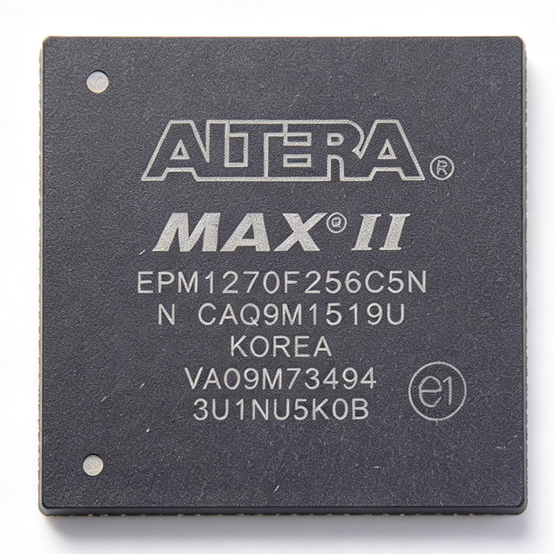
EPM1270F256C5N - MAX II 980-Macrocell CPLD | Intel | Altera
The Intel / Altera EPM1270F256C5N is a 980-macrocell, non-volatile, instant-on CPLD from the MAX II family, fabricated on a 0.18-µm process and housed in a 256-ball FineLine BGA package. It integrates 1270 logic elements, 980 macrocells, and 212 user I/O pins with a 6.2 ns pin-to-pin delay and a 201.1 MHz internal frequency. The device supports dual-voltage operation at 2.5 V / 3.3 V, making it compatible with both 2.5 V and 3.3 V logic families on the same board. The EPM1270F256C5N belongs to the MAX II family of instant-on, non-volatile CPLDs based on a 0.18-micron process and is supplied in a 256-FBGA tray. The 'N' suffix denotes a lead-free / Pb-free finish per industry lead-free marking conventions. A CPLD (Complex Programmable Logic Device) is a non-volatile programmable logic IC that combines AND/OR array-based macrocell architecture with on-chip flash configuration memory, providing instant-on behavior at power-up without an external boot ROM. Within the broader programmable logic hierarchy, CPLDs sit between small SPLDs/GALs and larger FPGAs, and are widely used as glue logic, I/O expanders, bus interface bridges, and power-up sequencers. MAX II CPLDs added low power consumption (multi-core architecture with internal flash) and integrated features such as user flash memory and a JTAG-based programming interface, making them a preferred choice for cost-sensitive control plane logic. Key features of the EPM1270F256C5N include non-volatile flash configuration for instant-on operation (no boot PROM required), 8 Kbits of user flash memory (per MAX II family), a JTAG-compliant IEEE 1149.1 boundary-scan / ISP interface, multi-voltage I/O support, and a chip-wide DEV_OE output enable pin. Multi-core architecture distributes logic across four logic regions, simplifying place-and-route for designs targeting fast pin-to-pin timing. Typical applications include I/O expansion and glue logic in 3.3 V and 2.5 V mixed-voltage systems, power-up sequencing for FPGAs and processors, JTAG-controlled bus bridges, address decoding for memory subsystems, and logic replacement for discrete 74-series TTL/MSI gates. The 256-FBGA package exposes 212 user I/O, allowing direct fan-out for dense parallel buses without external transceivers. When designing with this device, allocate sufficient PCB area for the 256-ball 1.0 mm pitch FBGA and follow Intel/Altera's reflow profile for lead-free BGA assembly. Use Quartus II software for HDL entry, synthesis, fitting, and timing closure; the same design can be retargeted across other MAX II family members with the same 256-pin footprint, simplifying board reuse. This page synthesizes distributor pricing, drop-in alternatives, and practical design notes not found in the manufacturer datasheet.
EPM1270F256I5 - 980-Macrocell MAX II CPLD, 256-FBGA | Altera
The Altera (Intel) EPM1270F256I5 is a MAX II family Complex Programmable Logic Device (CPLD) integrating 980 macrocells, 212 user I/O pins, and 8 Kbits of user flash memory in a 256-ball FineLine BGA (FBGA) package. It uses a 0.18 µm process and supports 2.5 V and 3.3 V I/O operation with 1.8 V core. The device provides a maximum internal operating frequency of approximately 201.1 MHz and a pin-to-pin propagation delay of approximately 6.2 ns. A CPLD (Complex Programmable Logic Device) is a non-volatile programmable logic device that combines multiple PAL/GAL-style macrocell blocks on a single chip with a global interconnect fabric. In the system hierarchy it sits between simple PLDs and FPGAs, offering instant-on non-volatile configuration, deterministic timing, and low power. MAX II specifically uses a Look-Up Table (LUT) based logic element, a flash-backed configuration cell, and a MultiTrack interconnect for predictable routing delays, making it a drop-in successor to legacy 5 V CPLDs. Key features of the EPM1270F256I5 include 980 logic elements, in-system programmability via JTAG, support for LVCMOS, LVTTL, PCI, SSTL-2, SSTL-3, and LVDS I/O standards, and an industrial temperature grade (-40 °C to +100 °C junction). The "I5" suffix denotes the industrial speed grade with tPD1 of 6.2 ns. The FBGA-256 package is surface-mount and provides high I/O density in a 17 mm × 17 mm footprint, making the device suitable for glue-logic and bus-interface consolidation where PCBs are constrained for space. Typical applications include I/O expansion and bridging in industrial controllers, power-sequencing and supervisory glue logic in telecom baseboards, bus decoding for legacy microprocessor interfaces, and configurable peripheral drivers. The instant-on behavior is particularly valuable in safety-critical or boot-time-sensitive systems that cannot tolerate FPGA configuration latency. Design consideration: the FBGA-256 package requires PCB design rules with 0.8 mm or 1.0 mm ball pitch, X-ray or rework-grade inspection for assembly, and at least four PCB layers for clean power/ground. Decoupling with 0.1 µF and 10 µF capacitors near each VCCIO/VCCINT ball is required. This page consolidates distributor pricing, drop-in same-family alternatives, and practical design guidance not found in the standalone MAX II datasheet.
EPM1270F256I5N - 980-Macrocell MAX II CPLD, 256-FBGA | Intel / Altera
The Intel / Altera EPM1270F256I5N is a 980-macrocell MAX II family Complex Programmable Logic Device (CPLD) housed in a 256-ball FineLine BGA (FBGA-256) package, built on a low-power 0.18-micron Flash-based process. It supports 212 user I/O pins, operates from 2.5 V / 3.3 V external supplies with 1.8 V core, and delivers 201.1 MHz maximum operating frequency with 6.2 ns pin-to-pin logic delay. The I5 speed grade combined with the -40C to +100C industrial temperature range makes this part suitable for demanding embedded control applications. A CPLD (Complex Programmable Logic Device) is a non-volatile programmable logic IC that sits between simple glue-logic PAL/GAL devices and larger FPGAs in the programmable logic hierarchy: CPLD -> programmable logic -> logic IC -> semiconductor. MAX II CPLDs use a unique MultiCore architecture pairing a LUT-based logic array with Flash configuration memory, providing instant-on behavior at power-up without external boot ROM - a key advantage over SRAM-based FPGAs in cost-sensitive and power-constrained designs. Key features include 980 macrocells (1270 logic elements), 8 Kbits user Flash memory, JTAG IEEE 1149.1 boundary-scan and in-system programmability via JTAG, MultiVolt I/O supporting 1.5 V, 1.8 V, 2.5 V, and 3.3 V interfaces, and a dedicated 3.3 V PCI-compliant I/O bank. The on-chip voltage regulator accepts a single 3.3 V supply and generates the internal core voltage, simplifying power tree design compared to legacy 5 V CPLDs. Typical applications include bus-interface bridging, I/O expansion and voltage-level translation, power-up sequencing logic, and glue-logic consolidation replacing multiple discrete PAL/GAL devices. The instant-on Flash architecture and industrial temperature range make EPM1270F256I5N especially common in telecom line cards, industrial controllers, and automotive infotainment subsystems where deterministic boot behavior is mandatory. When designing with this part, provide a minimum of four PCB layers with continuous ground and power planes for the FBGA-256 ball field, and use the Quartus II (or Quartus Prime Lite) design suite with a USB-Blaster or ByteBlaster for JTAG programming. Decoupling: place 0.1 uF ceramic capacitors within 50 mil of every VCCIO/VCCINT ball group, plus a 10 uF bulk cap near the supply pins. This page synthesizes distributor pricing, drop-in same-family MAX II alternatives, and practical FBGA-256 PCB design notes not collected in a single place in the original Altera datasheet.
EPM1270T144A5N - MAX II CPLD, 980 Macro Cells, 144-TQFP | Intel
The Intel (formerly Altera) EPM1270T144A5N is a MAX II family Complex Programmable Logic Device (CPLD) delivering 980 macro cells and 1270 logic elements in a 144-pin TQFP (T144) surface-mount package. It features a maximum propagation delay of 6.2 ns and supports internal supply voltages of 2.5 V and 3.3 V with an operating supply range of 2.375 V to 3.6 V, making it well-suited for low-power glue-logic and bus-interface bridging in 3.3 V systems. A CPLD (Complex Programmable Logic Device) is a non-volatile programmable logic device that combines multiple PAL-like macrocell arrays with a centralized interconnect matrix. It sits in the programmable logic hierarchy between simple SPLDs (e.g. PAL/GAL) and high-density FPGAs. CPLDs are valued for deterministic timing, instant-on behavior from on-chip Flash configuration memory, and high I/O-count pin flexibility. As part of the MAX II family, the EPM1270T144A5N targets high-volume cost-sensitive applications where instant-on logic and zero-configuration-time boot are essential. Key features include 116 user I/Os, 8 Kbits of embedded Flash user memory, JTAG (IEEE 1149.1) and in-system programmability via the Altera/Intel Quartus toolchain, and a wide -40C to +125C operating temperature range. The automotive-grade temperature suffix ("A5") indicates this part is rated for AEC-Q100-style harsh-environment use, though formal automotive qualification status should be confirmed against the latest Intel product folder. The EPM1270T144A5N uses a non-volatile Flash-based Look-Up Table (LUT) architecture with a global low-skew interconnect, providing predictable pin-to-pin delays that simplify multi-board timing closure. Compared with SRAM-based FPGAs it requires no external boot PROM and powers up ready-to-run, which is a decisive advantage in industrial control and automotive subsystem designs. Typical applications include I/O expansion and bus bridging, power-sequencing and reset-distribution logic, LED and display control, industrial sensor aggregation, automotive body and infotainment glue logic, and consumer electronics control planes. Designers should allocate JTAG pins (TCK/TMS/TDI/TDO) and decoupling capacitors per the MAX II handbook, and verify Quartus II/Quartus Prime support for the EPM1270 device symbol before commit.
EPM1270T144C3N - MAX II 1270 LE CPLD, 144-pin TQFP | Intel
The Intel (formerly Altera) EPM1270T144C3N is a low-power, non-volatile MAX II Complex Programmable Logic Device (CPLD) with 1270 logic elements, housed in a 144-pin TQFP package. Operating from a single 1.8 V core supply (VCCINT) with 3.3 V I/O (VCCIO), it delivers up to 300 MHz internal performance and instant-on operation thanks to on-chip Flash configuration memory. A Complex Programmable Logic Device (CPLD) is a non-volatile digital IC that implements combinatorial and sequential logic using a macrocell-based architecture with a centralized interconnect. CPLDs sit below FPGAs in the programmable logic hierarchy (CPLD -> PLD -> programmable logic -> digital IC), offering deterministic timing, instant-on configuration, and high drive strength ideal for glue logic, bus bridging, and power-up sequencing. Key features include 1270 logic elements (LEs), 980 equivalent macrocells, 8 Kbits of user Flash memory (UFM), 212 maximum user I/O pins, and MultiVolt I/O support for 1.5 V, 1.8 V, 2.5 V, 3.3 V interfaces. The device supports in-system programmability via IEEE 1149.1 JTAG and IEEE 1532, and offers 4-input look-up tables (LUTs) per logic element. Architecturally, the EPM1270 uses a classic MAX II LAB (Logic Array Block) structure with 16 macrocells per LAB, fast propagation delays (~3.6 ns pin-to-pin at -3 speed grade), and low standby current (~29 mA typical). The on-chip UFM supports up to 8 Kbits of non-volatile user storage, eliminating the need for external EEPROM for parameter storage. Typical applications include bus-interface bridging (e.g., 8/16/32-bit MCU-to-peripheral glue logic), power-up sequencing for FPGAs/ASICs, LED control and display driving, I/O expansion for microcontrollers, and replacement of multiple discrete 74-series logic gates. The wide MultiVolt I/O makes it ideal for mixed-voltage system designs. When designing with this device, evaluate total I/O count against the 212-pin maximum, and derate by at least 10% for routing flexibility. Always use the Quartus II or Intel Quartus Prime design software (free Web Edition) for synthesis, fitting, and JTAG programming. The T144 suffix denotes the 144-pin TQFP package; alternate package options (100-pin TQFP, 256-pin FineLine BGA) are available in the same EPM1270 die family. This page synthesizes distributor pricing, drop-in alternatives, and practical design notes not found in the manufacturer datasheet alone, providing engineers with a single reference for sourcing, replacement, and application guidance.
EPM1270T144C4N - MAX II CPLD 980 LE 144-TQFP | Intel / Altera
The Intel / Altera EPM1270T144C4N is a MAX II family Complex Programmable Logic Device (CPLD) delivering 980 logic elements (LEs) in a 144-pin TQFP package with 2.5 V / 3.3 V mixed-voltage I/O support and a 247.5 MHz internal core frequency. The "T144" suffix confirms the 144-pin TQFP plastic thin quad flat pack, the "C4" suffix denotes the commercial speed grade and 0.7 mm lead pitch, and the trailing "N" indicates a lead-free, RoHS-compliant assembly. A CPLD (Complex Programmable Logic Device) is a non-volatile, instantly-on programmable logic device that sits between a small FPGA and discrete glue logic in the system architecture hierarchy: CPLD -> programmable logic -> digital IC -> semiconductor. Unlike microcontrollers that execute sequential firmware, a CPLD runs parallel hardware state machines implemented in Look-Up Tables (LUTs) and macro cells, providing deterministic sub-nanosecond pin-to-pin propagation delays. MAX II devices in particular use a 1.8 V internal core with on-chip Flash configuration memory, eliminating the external boot PROM that legacy CPLDs required. Key features include 980 logic elements organized into 16 Logic Array Blocks (LABs), 80 user I/O pins, 8 Kbits of user Flash memory, on-chip voltage regulators supporting 3.3 V / 2.5 V / 1.8 V operation, JTAG IEEE 1149.1 boundary-scan support, and MultiVolt I/O allowing interfacing to 1.5 V, 1.8 V, 2.5 V, and 3.3 V logic without external level shifters. The MAX II architecture also embeds the Altera MultiTrack interconnect and delivers low dynamic power dissipation. Architecturally, MAX II combines LUT-based logic with a non-volatile Flash configuration cell so designs are always ready at power-up with no external boot device. The 144-TQFP package offers mature surface-mount assembly compatibility with conventional reflow profiles and supports vertical migration within the same package across the EPM570 / EPM1270 / EPM2210 density steps, allowing designers to scale logic capacity without changing PCB footprints. Typical applications include bus-bridging glue logic between processors and peripherals, I/O expansion for microcontrollers and ASICs, power-sequencing and reset distribution in multi-rail systems, configuration of FPGAs and memories, LED driving and display control, and protocol-bridging glue such as SPI-to-I2C or RGB-to-LVDS conversion. When designing with this device, leave at least 10% of logic resources unused to ease place-and-route and avoid timing closure issues. JTAG chain order must be planned carefully when the EPM1270T144C4N shares a scan chain with other boundary-scan devices, and unused I/O pins should be configured as outputs driving logic low rather than left floating. This page synthesizes distributor pricing, drop-in alternatives drawn from the MAX II family, and practical design notes not found in the manufacturer datasheet alone.
EPM1270T144C5N - MAX II CPLD, 980 LEs, 212 I/O, TQFP-144 | Intel/Altera
The Intel/Altera EPM1270T144C5N is a member of the MAX II family of Complex Programmable Logic Devices (CPLDs) delivering 980 Logic Elements (LEs), 980 macro cells, and up to 212 user I/Os in a 144-pin TQFP (T144) package. Built on a 0.18 µm flash-based process, it combines non-volatile configuration storage with low-power operation, providing instant-on functionality without an external boot PROM. The device is offered in the commercial 0 °C to +85 °C temperature range with a speed grade of -5. A CPLD (Complex Programmable Logic Device) is a non-volatile programmable logic device that sits between discrete glue logic and FPGAs in the programmable logic taxonomy. It uses a classic AND/OR PLA architecture with non-volatile flash cells, which means the configuration is retained across power cycles and the device begins operation within microseconds of power-up. The MAX II family specifically replaced Altera's legacy MAX 3000/7000 series by integrating flash configuration into the core, eliminating the need for an external configuration memory device and reducing total board cost and complexity. Key specifications include a maximum internal operating frequency of approximately 201.1 MHz, propagation delay (tPD) of 6.2 ns, a global clock network with up to 4 clocks per device, and supply voltage support for both 2.5 V and 3.3 V core/IO rails. The TQFP-144 package provides ample I/O for high-pin-count glue-logic applications, while JTAG (IEEE 1149.1) and in-system programmability via Altera/Quartus support simplified board-level bring-up and field upgrades. Typical applications include I/O expansion and bus bridging for microcontrollers, address decoding and glue logic in industrial control systems, power-sequencing and reset distribution, and LED-driving or display interface multiplexing. Because the configuration is non-volatile, the device operates without code shadowing or bootloader delay, making it well suited to deterministic boot-time applications. When designing with this part, account for I/O bank supply grouping (VCCIO banks) and ensure the Quartus II fitter report is reviewed to confirm pin assignment and timing closure before board sign-off.
EPM1270T144I5N - MAX II CPLD, 980 Macrocells, 144-TQFP | Intel
The Intel (formerly Altera) EPM1270T144I5N is a MAX II family Complex Programmable Logic Device (CPLD) delivering 980 macrocells and up to 212 user I/O pins, housed in a 144-pin TQFP (TQ) package. It operates at a core voltage of 2.5V/3.3V with multi-voltage I/O support (1.5V, 1.8V, 2.5V, 3.3V) and offers non-volatile Flash configuration memory with in-system programmability via JTAG. A CPLD (Complex Programmable Logic Device) is a non-volatile programmable logic device that sits between discrete glue logic and FPGAs in the programmable logic hierarchy. It provides instant-on operation, deterministic timing, and high-drive I/O for bus bridging, interface translation, and control-plane tasks. CPLDs belong to the broader family of programmable logic devices (PLDs), alongside FPGAs, and are commonly used as "glue logic" between processors, memory, and peripherals. Key features include 980 macrocells across 16 logic array blocks (LABs), 212 user I/Os, 8K bits of user Flash memory, and a maximum operating frequency of 201.1 MHz. The device provides multi-voltage I/O support, JTAG-based in-system programmability (ISP), and instant-on non-volatile operation. The industrial temperature range (-40C to +100C, "I" grade) and TQFP-144 package make it suitable for space-constrained, thermally-challenged designs. Architecturally, the MAX II family uses a low-power CMOS process with a uniform 4-input look-up table (LUT) architecture and a fast Global Clear signal. Unlike SRAM-based FPGAs, MAX II CPLDs require no external boot PROM and configure in microseconds, simplifying board layout and reducing BOM cost. Typical applications include I/O expansion and bus bridging for microcontrollers, power-up sequencing logic, peripheral interface glue logic (SPI, I2C, UART, parallel bus), and control-plane state machines in industrial and consumer systems. The combination of low cost, low power, and high I/O count also makes it attractive for prototype and small-volume production designs. Design considerations include thermal management for the 144-pin TQFP, I/O bank voltage planning (each bank can be powered independently to 1.5V/1.8V/2.5V/3.3V), and proper JTAG chain configuration. Quartus II software (or the free Quartus Prime Lite Edition) is required for design entry, synthesis, and programming. This page synthesizes distributor pricing, drop-in same-package alternatives, and practical design notes not found on the manufacturer datasheet alone, helping engineers select the optimal MAX II variant for their application.
EPM1270TI144C5N - 980 Macro Cell CPLD, MAX II, 144-TQFP | Intel
The Intel (formerly Altera) EPM1270TI144C5N is a non-volatile, flash-based Complex Programmable Logic Device (CPLD) from the MAX II family, delivering 980 macro cells, 212 user I/O pins, and a 6.2 ns pin-to-pin logic delay in a 144-pin TQFP package. It is built on a low-power 0.18 µm process and operates from a 2.5 V/3.3 V dual-voltage core/I/O supply, with internal flash configuration memory providing instant-on capability and eliminating the need for external boot ROM. The part is the industrial temperature range variant of the MAX II EPM1270, supporting -40 °C to +100 °C ambient operation. A CPLD (Complex Programmable Logic Device) is a non-volatile digital logic IC that combines the deterministic timing of PAL/GAL architecture with on-chip flash configuration memory, enabling glue-logic, bus-bridging, I/O expansion, and power-up state-machine functions without an external boot device. Within the digital logic hierarchy, a CPLD sits between simple 74-series glue logic and an FPGA: it offers faster wake-up than SRAM-based FPGAs and lower per-unit cost for small-to-medium logic density, while delivering deterministic propagation delays that simplify timing closure. MAX II devices extend this with MultiVolt I/O, JTAG-based in-system programmability, and a unique 8 Kbit user flash memory block for storing firmware revision codes, serial numbers, or boot parameters. Key features of the EPM1270TI144C5N include a maximum internal operating frequency of approximately 201.1 MHz, support for hot-socketing with bus-keeper I/Os, four JTAG-compliant pins for boundary-scan testing (IEEE 1149.1), MultiVolt core allowing the device to interface with 1.5 V, 1.8 V, 2.5 V, and 3.3 V logic without level shifters, and a built-in real-time in-system programmability feature that supports field upgrades. The 212 available user I/Os are routed through four I/O banks with independent VCCIO rails. Typical applications include I/O expansion and bus bridging in industrial controllers, power-up sequencing and reset logic for FPGA-based SoCs, peripheral interfacing in legacy equipment designs, and glue-logic replacement of multiple discrete 74-series TTL/CMOS parts. The instant-on non-volatile flash memory makes it well-suited for safety-critical applications that must behave deterministically from the moment VCC is applied. Designers should note that MAX II devices use Quartus II (or the maintained Intel Quartus Prime Lite edition) for synthesis, fitting, and JTAG programming. Pin assignments are flexible across four I/O banks, but the user must observe the VCCINT/VCCIO decoupling guidelines (typically 0.1 µF plus 10 µF bulk caps per bank) to meet the 6.2 ns tPD specification under full 212-I/O simultaneous-switching loads. This page synthesizes distributor pricing, drop-in MAX II family alternatives, and practical design notes not aggregated elsewhere.
EPM2210F256A5NGA - 2210 LE MAX II CPLD, 256-BGA | Intel
The Intel (Altera) EPM2210F256A5NGA is a MAX II family Complex Programmable Logic Device (CPLD) that delivers 2210 Logic Elements in a 256-ball FineLine BGA package, providing low-cost, non-volatile, low-power logic integration for glue-logic and I/O expansion designs. It features 1700 macrocells and 7 ns maximum pin-to-pin propagation delay per the manufacturer datasheet. The device targets applications where board space, instant-on non-volatility, and ultra-low standby power matter more than the highest logic density. A CPLD (Complex Programmable Logic Device) is a non-volatile programmable logic device that combines multiple PAL-like macrocell blocks on a single chip with a central interconnect. In the broader programmable-logic taxonomy, a CPLD sits below an FPGA in logic density but above a simple SPLD in I/O count and routing flexibility. MAX II devices are a specific Intel/Altera family that uses a 0.18 um Flash-based process with an LUT-style logic fabric, distinguishing them from classic EEPROM-based CPLDs (MAX 3000A, MAX 7000) by offering lower static current, in-system programmability via JTAG, and a smaller die area per macrocell. Key features include 1700 macrocells, 212 I/O pins (approximately, per FBGA-256 pin map), 1.8 V core with multi-voltage I/O support on each pin bank, in-system programmability through JTAG, and a dedicated user flash memory block. The part operates on a single 1.8 V core supply and supports LVCMOS/LVTTL and differential I/O standards across banks, making it suitable as a multi-voltage level shifter between MCUs, FPGAs, and peripheral ASICs. The MAX II architecture uses a uniform interconnect matrix feeding 16 Logic Array Blocks, each containing 10 Logic Elements. Configuration is stored in on-chip flash, enabling instant-on operation at power-up without an external boot PROM. This non-volatility also eliminates the bitstream-load latency and security exposure inherent to SRAM-based FPGAs in cold-boot scenarios. Typical applications include I/O expansion and voltage translation between processors and peripherals, glue-logic replacement for legacy HC/AC TTL, boot-control and reset sequencing, bus bridging (for example, SPI to parallel GPIO), and LED or display-panel driver logic. Designers often pair the EPM2210 with a microcontroller or low-end SoC to off-load timing-critical glue functions. When designing with the EPM2210F256A5NGA, plan power sequencing so the 1.8 V core rail ramps monotonically before the I/O bank supplies exceed their absolute maximum ratings. Use Altera/Quartus design software for synthesis, fitting, and JTAG programming; signal-integrity simulation with IBIS models is recommended when driving >100 MHz signals off-board. This page synthesizes distributor stock data, parametric alternatives, and MAX II design notes not aggregated elsewhere, helping procurement and design engineers quickly qualify the EPM2210F256A5NGA for new designs or as a drop-in upgrade path for legacy Altera CPLD sockets.
EPM2210F256C3N - MAX II CPLD 1700 Macrocells 7ns 256-FBGA | Intel
The Intel (formerly Altera) EPM2210F256C3N is a MAX II family Complex Programmable Logic Device (CPLD) delivering 1700 macrocells, 2210 logic elements, and 204 user I/Os in a 256-ball FineLine BGA package with a 7 ns maximum pin-to-pin propagation delay. It operates from internal 2.5V or 3.3V supplies, is in-system programmable via JTAG, and is rated for the commercial 0C to 85C operating junction temperature range. The MAX II architecture is built on a 0.18um flash-based process, providing instant-on non-volatile configuration that eliminates the external boot memory required by SRAM FPGAs. A CPLD (Complex Programmable Logic Device) is a non-volatile programmable logic device that combines multiple SPLD-like macrocell blocks on a single chip with a programmable interconnect matrix. In the system hierarchy it sits between simple SPLDs/PALs and full FPGAs: simpler than an FPGA (no boot PROM, deterministic timing), more capable than a SPLD (wider fan-in, more I/Os, more product terms). MAX II devices are positioned as low-cost, low-power glue-logic replacements for discrete 74-series logic and small FPGAs, and as I/O expanders for microcontrollers. Key features include 7 ns tPD (pin-to-pin), 304 MHz internal fMAX, JTAG-based IEEE 1149.1 in-system programmability, MultiVolt I/O supporting 1.5V/1.8V/2.5V/3.3V interfaces, an on-chip voltage regulator allowing single 3.3V supply operation, and zero standby current due to flash configuration. The FineLine BGA-256 package is shared vertically across the EPM570, EPM1270, and EPM2210 family, enabling PCB migration between densities. The MAX II architecture uses a Look-Up Table (LUT) + register macrocell, but unlike FPGAs the configuration is stored in on-chip flash rather than SRAM. This provides instant-on behavior at <100 us, deterministic timing (no jitter from configuration), and immunity to configuration bit upsets from radiation or noise. The device also embeds a User Flash Memory block (8 Kbits) accessible from the logic array for storing revision IDs or calibration constants. Typical applications include I/O expansion and bus bridging for microcontrollers, address decoding and glue logic in embedded systems, power-sequencing and reset-distribution networks, LED display multiplexing and industrial control front panels, and portable/battery-powered systems where the instant-on behavior and low standby power of the MAX II flash process deliver clear advantages over SRAM-based FPGAs. When designing with the EPM2210F256C3N, follow Altera/Intel MAX II hardware design guidelines: route JTAG TMS/TCK/TDO/TDI to a clean header, use a 100 ohm differential impedance for high-speed outputs, and provide adequate decoupling (100 nF + 10 uF per supply pin pair) near the BGA balls. This page synthesizes distributor pricing, drop-in MAX II family alternatives, and practical MAX II design notes not found in the manufacturer datasheet alone, helping engineers select and source the right CPLD density, speed grade, and temperature grade for their application.
EPM2210F256C4 - 2210 LE MAX II CPLD, 256-FBGA | Altera
The Altera (Intel) EPM2210F256C4 is a MAX II family Complex Programmable Logic Device (CPLD) that delivers 2,210 logic elements (equivalent to 1,700 macrocells) in a 256-ball FineLine BGA package. Built on a 0.18 µm six-layer-metal flash process, it provides non-volatile storage of configuration in 8 Kbits of on-chip flash memory, supporting instant-on behavior without an external boot PROM. The device operates across a 1.8 V core / 2.5 V or 3.3 V I/O MultiVolt interface, with commercial extended temperature grading. What is a CPLD? A Complex Programmable Logic Device is a non-volatile programmable logic IC that bridges the gap between discrete 74-series glue logic and FPGAs. CPLDs typically feature instant-on, deterministic timing, wide input gating, and modest logic density (hundreds to a few thousand macrocells). The MAX II architecture positions the family at the high-density end of the CPLD hierarchy: CPLD -> non-volatile programmable logic -> programmable logic IC -> digital semiconductor. The 'LE' (logic element) count is a vendor-specific unit; for MAX II, 1 LE ≈ 1.3 macrocells, which is why the 2,210-LE device is described as 1,700 macrocells. Key features include 1.8 V core supply with MultiVolt I/O supporting 1.5 V, 1.8 V, 2.5 V, and 3.3 V interfaces, an 8 Kbit User Flash Memory (UFM) block for non-logic data storage, JTAG-based in-system programmability (ISP), and 212 user I/O pins. The internal 7 ns pin-to-pin propagation delay (tPD1) supports glue-logic and bus-interface bridging at frequencies up to approximately 201 MHz. Typical applications include bus interface bridging, I/O expansion and voltage translation, power-up and power-sequencing control, configuration of larger FPGAs, and glue-logic replacement on industrial, telecom, and consumer motherboards. The UFM block additionally supports small-data EEPROM-style storage such as revision IDs, calibration tables, or boot parameters. When designing with the EPM2210F256C4, treat the 256-ball FineLine BGA as a fine-pitch package and follow standard BGA PCB design rules: microvia or via-in-pad recommended, matched-length impedance for high-speed edges, and proper thermal relief for the center balls that sit beneath the die. Quartus II (or the current Quartus Prime Lite) is the supported design entry and programming toolchain. This page synthesizes distributor pricing, drop-in alternatives within the same MAX II family, and practical design notes not found in the manufacturer datasheet alone.
EPM2210F256C4N - 2210 LE MAX II CPLD 256-FBGA | Intel / Altera
The Intel (formerly Altera) EPM2210F256C4N is a MAX II family Complex Programmable Logic Device (CPLD) integrating 2,210 Logic Elements (LEs), 1,700 macro cells, and 204 Kbits of user flash memory into a 256-ball FineLine BGA (FBGA) package. Built on a 0.18 µm process, it offers a maximum internal operating frequency of 247.5 MHz, a pin-to-pin propagation delay of 7.0 ns, and supports I/O standards including 3.3-V LVTTL/LVCMOS, 2.5-V LVTTL/LVCMOS, 1.8-V LVTTL/LVCMOS, 1.5-V LVCMOS, and PCI up to 66 MHz. The device is supplied by a 3.3 V core / I/O rail and operates over the commercial 0 °C to +85 °C temperature range. A Complex Programmable Logic Device (CPLD) is a non-volatile, instant-on programmable logic IC that combines multiple PAL/GAL-like macro-cell arrays with a global interconnect fabric. It belongs to the broader class of programmable logic devices (PLD), which also includes FPGAs; CPLDs are distinguished by deterministic timing, low static power, and flash-based configuration that eliminates external boot memory. Within the MAX II family, the EPM2210 is the highest-density member, positioning it between small glue-logic CPLDs and entry-level FPGAs. Key features include four global clock networks with up to four clock pins, a JTAG-compliant IEEE Std. 1149.1 boundary-scan interface with in-system programmability (ISP), 8 Kbits of user flash memory, MultiVolt I/O for mixed-voltage interfacing, and on-chip support for 32-bit, 66-MHz PCI. The 256-ball FineLine BGA package is pin-compatible with EPM570F256 and EPM1270F256 devices, enabling vertical density migration without PCB rework. The EPM2210F256C4N is widely used as a bus-bridging glue-logic replacement, an I/O expansion controller for microcontrollers, a power-up sequencer for multi-rail systems, and a low-density state-machine engine in industrial, consumer, and automotive subsystems. Designers favor the MAX II family for its instant-on non-volatile behavior, predictable timing, and Quartus Prime Lite design-flow support. When integrating this part, ensure 1.2 V, 2.5 V, and 3.3 V supplies are decoupled with 0.1 µF and 10 µF capacitors placed within 100 mils of each ball. Maintain continuous reference planes beneath the BGA and follow Altera's JTAG chain guidelines for in-system programming. This page synthesizes distributor pricing, drop-in same-package alternatives, and practical MAX II design notes not aggregated in any single manufacturer datasheet.
EPM2210F256C5 - MAX II CPLD 1700 Macrocells 201MHz FBGA-256 | Altera / Intel
The Altera / Intel EPM2210F256C5 is a MAX II family Complex Programmable Logic Device (CPLD) offering 1700 macrocells, 201.1 MHz maximum internal frequency, and a 256-ball FineLine BGA (FBGA-256) package. It is fabricated on a 0.18 µm flash-based process and supports both 2.5 V and 3.3 V operation, making it a flexible glue-logic replacement for multiple discrete SSI/MSI parts. A CPLD (Complex Programmable Logic Device) is a non-volatile, flash-programmable logic device that sits between simple SPLDs and FPGAs in the programmable logic hierarchy: SPLD -> CPLD -> FPGA -> Programmable Logic. MAX II devices are particularly valued for their instant-on (no boot PROM required), ultra-low standby current, and high I/O count, and they are commonly used for I/O expansion, bus bridging, and power-up sequencing in designs that also include an FPGA, ASIC, or microprocessor. Key features of the EPM2210F256C5 include 1700 logic elements (macrocells), 272 user I/Os, instant-on non-volatile configuration stored in on-chip flash, in-system programmability via JTAG (IEEE 1149.1), and a MultiVolt core allowing I/O bank operation from 1.5 V to 3.3 V. The device supports commercial-grade operating temperature 0C to +85C (C5 suffix) and vertical migration within the 256-ball FBGA package alongside the smaller EPM570F256 and EPM1270F256 devices. Architecturally, the EPM2210F256 uses Altera's classic Lab/Expander-matrix interconnect feeding Logic Array Blocks (LABs) of 16 macrocells each, with each macrocell containing a programmable flipflop and a wide sum-of-products engine. Combined with the on-chip User Flash Memory (UFM) block, this enables system designers to store board parameters, serial numbers, or boot configuration without an external EEPROM. The 201 MHz fMAX is derived from a 5 ns internal propagation delay and is typical for the C5 speed grade. Typical applications include I/O expansion and level translation between legacy 5 V/3.3 V peripherals and modern processors, FPGA I/O bank expansion, board-level glue logic replacement, bus protocol bridging (e.g., SPI to parallel), power-rail sequencing at system start-up, and embedded control where deterministic propagation delay matters more than raw throughput. When designing with the EPM2210F256C5, leave a generous copper pour under the exposed thermal pad (if any), ensure all JTAG signals (TCK, TMS, TDI, TDO) are pulled to defined logic states, and verify VCCINT and VCCIO decoupling with 0.1 µF capacitors placed as close to each supply pin as possible. The C5 commercial speed grade is not interchangeable with C3/C4/I4/I5 grades without recompiling the design. This page synthesizes distributor pricing, MAX II drop-in alternatives, vertical-migration guidance, and practical design notes not found in the bare Altera datasheet - useful for BOM managers and hardware engineers evaluating legacy MAX II designs.
EPM2210F256C5N - 2210 LE, 1700 Macrocells MAX II CPLD | Intel
The Intel (Altera) EPM2210F256C5N is a non-volatile, flash-based Complex Programmable Logic Device (CPLD) from the MAX II family, featuring 2210 logic elements and 1700 macrocells in a 256-ball FineLine BGA package (17x17mm, 1mm pitch). The device delivers a typical propagation delay of 7ns, turn-on delay of 11.2ns, and a maximum internal operating frequency of 201.1MHz, powered by a 2.375V-to-3.6V (3.3V typical) supply. A CPLD (Complex Programmable Logic Device) is a non-volatile programmable logic device that provides instant-on operation, deterministic timing, and high I/O count glue logic for digital systems. CPLDs sit in the programmable logic hierarchy between simple SPLDs and large FPGAs, occupying a role historically filled by discrete 74-series logic gates, address decoders, and bus interface devices. The MAX II family specifically targets low-power, low-cost, high-volume glue-logic replacement with on-chip flash configuration memory. Key features of the EPM2210F256C5N include 204 user I/Os, MultiVolt core supporting 1.5V/1.8V/2.5V/3.3V I/O standards, four global clocks with eight clock pins, and an on-chip voltage regulator for single-supply operation. The 8Kbits of user flash memory (UFM) provides non-volatile storage for user data, eliminating external EEPROM. The 'C5' speed grade combined with the commercial 0C to 85C operating range makes this part the mainstream cost-optimized variant. The MAX II architecture uses a 0.18um CMOS process with a unique MultiTrack interconnect scheme, reducing die size while maintaining predictable timing. Unlike SRAM-based FPGAs that require external boot PROMs, the on-chip flash configuration makes MAX II devices instant-on at < 1ms, ideal for systems that cannot tolerate FPGA configuration latency. The 256-FBGA package supports high-density board designs with exposed pads for thermal dissipation. Typical applications include I/O expansion and bus bridging in industrial controllers, address decoding and timing adjustment in telecom equipment, power-up sequencing logic in networking switches, and glue-logic consolidation in medical and test instruments. The wide I/O voltage range allows direct interfacing to legacy 5V-tolerant busses via resistor networks. When designing with this part, use Altera (now Intel) Quartus II design software version 13.0 or later for synthesis, fitting, and programming file generation. The JTAG interface supports both IEEE 1149.1 boundary-scan testing and in-system programming via the ByteBlaster or USB-Blaster download cables. This page synthesizes distributor pricing, drop-in alternatives from the same MAX II family, and practical design notes not aggregated on any single distributor product page.
EPM2210F256I5 - MAX II CPLD, 1700 Macrocells, 201MHz | Altera
The Altera (Intel) EPM2210F256I5 is a high-density MAX II family Complex Programmable Logic Device (CPLD) featuring 1700 macrocells and 2210 logic elements, housed in a 256-ball FineLine BGA package. It operates with internal supply voltages of 2.5V and 3.3V and delivers a maximum internal frequency of 201.1 MHz with a maximum propagation delay (tpd) of 7.0 ns. What is a CPLD? A CPLD (Complex Programmable Logic Device) is a non-volatile programmable logic device that sits between simple PAL/GAL devices and high-density FPGAs. CPLDs use flash-based or EPROM configuration memory, providing instant-on operation, deterministic timing, and excellent pin-to-pin consistency. The MAX II family hierarchy is: CPLD -> Programmable Logic -> Logic IC -> Integrated Circuit, and EPM2210F256I5 is the largest density member of the MAX II generation. Key features of the EPM2210F256I5 include 1700 macrocells distributed across 16 logic array blocks, an 8 Kbit user flash memory block, JTAG and in-system programmability via Altera's ByteBlaster or USB-Blaster, multi-volt I/O supporting 1.5V, 1.8V, 2.5V, and 3.3V interfaces, and 4 JTAG-compliant pins (TCK, TMS, TDI, TDO). The device supports the IEEE 1149.1 boundary-scan standard for board-level testability. Technically, the EPM2210F256I5 implements a Logic Array Block (LAB) architecture where each LAB contains 16 macrocells with interconnect via the MultiTrack interconnect. The multi-volt core allows the device to interface with legacy 5V-tolerant systems while drawing low standby current, which is critical for power-sensitive glue-logic applications. The MAX II architecture also provides an instant-on capability with no external boot memory required. Typical applications include I/O expansion and bridging in industrial controllers, register and state-machine implementation in FPGA co-processing, configuration logic for memory and peripherals, glue-logic replacement for discrete 74-series TTL, and bus interface translation in legacy system upgrades. The wide temperature range makes it suitable for industrial automation, telecommunications line cards, and white-goods control boards. When designing with this part, note that MAX II devices support vertical migration within the same package: EPM570, EPM1270, and EPM2210 share the 256-pin FineLine BGA footprint, allowing PCB reuse across density options. Designers should also ensure the Quartus II or Intel Quartus Prime software is configured for MAX II support before compilation. This page synthesizes distributor pricing, drop-in alternatives, and practical design notes not found in the manufacturer datasheet alone, giving engineers an at-a-glance comparison between EPM2210F256I5 and its vertical-migration siblings.
EPM2210F324C3N - 2210 LE MAX II CPLD, 7ns, 324-FBGA | Intel
The Intel (formerly Altera) EPM2210F324C3N is a MAX II family Complex Programmable Logic Device (CPLD) featuring 2,210 logic elements (equivalent to 1,700 macrocells), 8 Kbits of non-volatile flash UFM storage, and a 7 ns pin-to-pin logic delay, housed in a 324-ball FineLine BGA (FBGA-324) package with 1.0 mm ball pitch and 19 x 19 mm body. It is fabricated on a low-power 6-layer-metal CMOS flash process and operates from a 1.8 V core with MultiVolt I/O supporting 1.5 V, 1.8 V, 2.5 V, 3.0 V, and 3.3 V interfacing. What is a CPLD? A Complex Programmable Logic Device is a non-volatile programmable logic IC that combines the instant-on, deterministic behavior of traditional PAL/GAL architectures with higher logic density, in-system flash programmability (ISP), and integrated user flash memory. Within the programmable logic hierarchy (CPLD -> programmable logic -> digital IC -> semiconductor), MAX II devices target glue-logic, interface bridging, and power-up controller applications where instant-on non-volatile configuration is essential and FPGA-class densities are not required. Key features include 272 maximum user I/Os, 4 global clock networks, JTAG 1149.1 boundary-scan support, and on-chip flash configuration memory that eliminates external boot PROMs. The integrated UFM block (8 Kbits) provides non-volatile parameter storage accessible through dedicated interface logic, replacing small EEPROMs in many designs. Enhanced in-system programmability (ISP) and a built-in Joint Test Action Group (JTAG) interface enable rapid prototyping and field upgrades. The MAX II architecture uses a Logic Array Block (LAB) matrix connected by a MultiTrack interconnect, with each LAB containing 16 Logic Elements (LEs). Each LE combines a 4-input LUT, a programmable register, and dedicated carry/control logic, delivering 7 ns tPD1 propagation delay at industrial temperature and voltage corners. Typical applications include bus-interface bridging (e.g., 8-bit MCU to 16/32-bit peripheral), power-up sequence controllers, I/O expansion for ASSPs, LED display multiplexing, and configuration EEPROM replacement. Designers choose the EPM2210F324C3N when instant-on non-volatile logic, low standby power, and the highest I/O count in the MAX II family are required in a compact 19 x 19 mm BGA footprint. Design consideration: the FBGA-324 package requires careful PCB layout with microvia or via-in-pad technology for reliable assembly; verify the PCB fabrication capability before committing to this package. Quartus II (legacy) or Quartus Prime (current) software is required for design entry, synthesis, and programming - ensure toolchain support is available. This page synthesizes distributor pricing, MAX II family cross-references, and PCB-level design notes not found in a single manufacturer document, enabling faster sourcing and replacement decisions for engineers and procurement teams.
EPM2210F324I8N - MAX II CPLD 2210 LE F324 Industrial | Altera
The Altera (now Intel) EPM2210F324I8N is a MAX II family CPLD delivering 2210 logic elements with non-volatile, instant-on configuration in a 324-pin F324 FineLine BGA package, industrial temperature grade. It features 25 µA typical standby current, fast propagation delay, and clock-to-output times for glue-logic and I/O expansion roles. A CPLD (Complex Programmable Logic Device) is a non-volatile programmable logic IC that retains its configuration without an external boot PROM. MAX II devices are built on a 0.18-micron process and pair LUT-based logic with on-chip Flash configuration memory. They sit below FPGAs in the programmable logic hierarchy (CPLD -> programmable logic -> logic IC -> semiconductor), offering deterministic timing, low quiescent current, and instant-on behavior for system control, bus bridging, and power-sequencing tasks. Key features of the EPM2210F324I8N include 2210 logic elements (LEs), 272 user I/O pins, on-chip user flash memory, 8 Kbits of configuration memory in the same die, support for multiple I/O standards (LVTTL, LVCMOS, PCI, SSTL), and an internal oscillator. The instant-on, non-volatile architecture eliminates boot PROM cost and enables configuration in <1 ms. Multi-voltage I/O banks allow the part to bridge 1.5V, 1.8V, 2.5V, 3.3V, and 5.0V domains on the same board. Architecturally, MAX II uses a four-input LUT fabric with 16 macrocell Logic Array Blocks (LABs) connected through a MultiTrack interconnect. The integrated Flash and SRAM block stores both configuration and user data, supporting in-system programmability via JTAG. Compared with older MAX 3000/7000 families, MAX II cuts standby current by an order of magnitude while preserving JTAG and IEEE 1149.1 boundary-scan compatibility. Typical applications include I/O expansion and bus bridging, power-up sequencing and reset distribution, industrial control boards, motor drive interface logic, and LED display drivers. The 324-pin package and 272 user I/Os support designs that require many LVCMOS channels with deterministic propagation delays. When designing with this device, allocate JTAG pins (TCK, TMS, TDI, TDO) carefully and provide at least four general-purpose I/Os for ISP updates. For high-toggle-rate outputs, derate bank current per the Quartus II power-play estimator and verify pin-to-pin timing via TimeQuest before sign-off. This page synthesizes distributor pricing, MAX II family drop-in alternatives, and practical Quartus II design notes not found in the manufacturer datasheet, helping engineers select, source, and implement the EPM2210F324I8N with confidence.
EPM2210GF256C5N - MAX II CPLD, 2210 LEs, 256-FBGA | Intel / Altera
The Intel (formerly Altera) EPM2210GF256C5N is a MAX II family Complex Programmable Logic Device (CPLD) featuring 2210 Logic Elements housed in a 256-ball FineLine BGA package with commercial temperature grade and a C5 speed grade. As the highest-density member of the MAX II instant-on, non-volatile family, it is built on a 0.18-micron process and offers up to 272 user I/O pins with multi-volt I/O support, enabling flexible interface bridging between 1.5V, 1.8V, 2.5V, 3.3V and LVDS signaling domains. A CPLD (Complex Programmable Logic Device) is a non-volatile programmable logic device containing multiple macrocells interconnected through a programmable interconnect matrix. Within the broader semiconductor taxonomy, a CPLD sits between simple PAL/GAL devices and larger FPGAs - it is non-volatile (retains configuration without external flash), instant-on (configures in microseconds rather than milliseconds), and well-suited to glue-logic, bus-bridging and control-plane tasks. MAX II devices belong to the power management IC's sibling family of programmable logic, fabricated on a 0.18-µm process node and storing their configuration in on-chip Flash memory. Key features include 2210 Logic Elements, 272 maximum user I/Os, 8 Kbits of user Flash memory, on-chip oscillator, and 4-input look-up table (LUT) based logic with a MultiTrack interconnect architecture. The C5 speed grade provides predictable timing suitable for glue logic, I/O expansion, and bus-interface applications. The MAX II architecture combines a non-volatile Flash configuration block with a LUT-based logic fabric, allowing instant-on behavior without an external configuration PROM. The MultiTrack interconnect minimizes routing congestion for wide buses, and the device supports in-system programmability via JTAG (IEEE 1149.1) with the Altera/Quartus toolchain. Typical applications include I/O expansion and voltage-translation bridges in industrial control boards, power-sequencing and supervisory logic in networking switches, instant-on glue logic replacing discrete 74-series logic in cost-sensitive consumer electronics, and bus-interface management between microcontrollers and peripheral ICs. When designing with this part, note that the GF256 package supports vertical migration within the same footprint across the EPM570, EPM1270, and EPM2210 density points, allowing board reuse with software-driven density scaling. Decoupling follows standard FPGA/CPLD guidelines: bulk capacitors on each supply rail plus high-frequency ceramic decoupling adjacent to each power pin. This page synthesizes distributor pricing, drop-in alternatives, and design notes that complement - but are not found within - the manufacturer datasheet alone.
EPM2210GF324C4N - 2210 LE MAX II CPLD 324-FBGA | Intel
The Intel EPM2210GF324C4N is a non-volatile, instant-on Complex Programmable Logic Device (CPLD) from the MAX II family, delivering 2,210 logic elements (approximately 1,700 equivalent macrocells) in a 324-ball FineLine BGA package. It operates from a 1.8 V core supply with MultiVolt I/O support for 1.5 V, 1.8 V, 2.5 V, 3.3 V, and 5.0 V mixed-voltage interfacing. The device is fabricated on a 0.18 µm 6-layer-metal flash process that provides instant-on configuration in less than 1 ms without external boot memory. A CPLD (Complex Programmable Logic Device) is a non-volatile programmable logic device that implements combinational and sequential logic via a fabric of AND-OR arrays and macrocells, sitting in the hierarchy between simple SPLDs and high-density FPGAs. CPLDs are typically used for glue logic, bus interface bridging, power-up sequencing, and state-machine control where deterministic timing, instant-on behavior, and high I/O counts matter more than the millions of LUTs offered by an FPGA. The MAX II family in particular replaces legacy EEPROM-based CPLDs with a flash-backed architecture that integrates an 8 Kbit User Flash Memory (UFM) block for on-chip parameter storage. Key features include 272 user I/Os (maximum), 247.5 MHz internal performance, 7 ns pin-to-pin logic delay (commercial -4 speed grade), in-system programmability via IEEE 1149.1 JTAG, and built-in boundary-scan support. The 324-pin FineLine BGA exposes the widest I/O count in the MAX II family, allowing direct replacement of multiple 74-series logic packages or older MAX 7000-series devices. The flash-based configuration makes the part tolerant of supply brown-outs without losing the bitstream. The internal architecture pairs a Lab/Logic Array Block (LAB) structure with each LAB containing 16 Logic Elements (LEs), interconnected via a MultiTrack interconnect. The embedded UFM block provides 8 Kbits of general-purpose non-volatile storage accessible through a dedicated interface, useful for storing board serial numbers, calibration coefficients, or default register values that must survive power cycling. Typical applications include bus interface bridging (for example, I2C-to-SPI or parallel-to-LVDS glue logic), power-up and power-down sequencing controllers for ASICs and processors, industrial fieldbus protocol glue logic, I/O expansion and level translation, and replacement of legacy discrete 74HC/74FTTL logic. Designers also use the device for state-machine-driven control in motor drives, instrumentation front-ends, and embedded computing boards where deterministic timing and instant-on are mandatory. When designing with this part, observe the I/O bank supply constraints: each bank must be powered before or coincident with VCCINT to avoid latch-up. Use the Quartus II or Intel Quartus Prime design software (free MAX II device support) for synthesis, fitting, and JTAG programming, and follow the IBIS models provided on intel.com for signal-integrity simulation of the FineLine BGA fan-out. This page synthesizes distributor pricing, drop-in MAX II alternatives in the same 324-ball BGA footprint, and practical design notes that go beyond the manufacturer datasheet to accelerate board bring-up.
EPM2210GF324C5 - MAX II 2210 LE CPLD, 324-BGA, 5ns | Intel/Altera
The Intel (formerly Altera) EPM2210GF324C5 is a non-volatile MAX II family Complex Programmable Logic Device (CPLD) with 2,210 logic elements (equivalent to 1,700 macrocells), 8 Kbits of on-chip user flash memory (UFM), and 272 maximum user I/Os. It is packaged in a 324-ball FineLine BGA (GF324) with 1.0 mm pitch and supports commercial-grade junction temperature operation. Key headline parameters: 5 ns pin-to-pin logic delay (tPD1), 1.8 V core voltage with MultiVolt I/O support (1.5 V, 1.8 V, 2.5 V, 3.3 V), 304 MHz internal performance, and JTAG-based in-system programmability (ISP). What is a CPLD? A Complex Programmable Logic Device is a non-volatile, instantly-on programmable logic device that sits between discrete glue logic and FPGAs in the digital design hierarchy: discrete logic -> PLD -> CPLD -> FPGA -> ASIC. Unlike SRAM-based FPGAs that require a configuration flash, a flash-based CPLD boots in microseconds and retains its bitstream through power cycles, making it ideal for power-up deterministic glue logic, bus bridges, and control-plane state machines. The EPM2210GF324C5 features MultiVolt core and I/O technology allowing the device to interface directly between 1.5 V, 1.8 V, 2.5 V, and 3.3 V logic domains without external level translators. The integrated 8-Kbit UFM block can be used for storing revision codes, serial numbers, or user-defined lookup tables accessible via an internal interface. Enhanced ISP via JTAG (IEEE 1149.1) and a built-in 4-wire interface simplify prototype bring-up and field updates. Architecturally, MAX II devices use a 6-layer-metal flash process with a Logic Array Block (LAB) structure of 16 macrocells each, connected through a fast MultiTrack interconnect. Compared to the legacy MAX 3000/7000 families, MAX II consumes roughly one-tenth the static power while delivering up to 2x the performance, a key reason it replaced older CPLDs in new designs through the late 2000s and early 2010s. Typical applications include I/O expansion and bus bridging in industrial controllers, power-up sequencing logic in telecom line cards, glue logic replacement in embedded processor designs, LED display drivers, and configuration control for multi-rail power systems. The wide MultiVolt I/O range makes it especially useful for mixed-voltage designs (e.g., bridging a 3.3 V MCU to 1.8 V peripherals). When designing with the EPM2210GF324C5, observe the 1.0 mm BGA pitch requirement - PCB assembly demands reflow profiles compatible with large fine-pitch BGAs, and signal escape routing under the array needs careful stack-up planning. Decoupling per VCCIO/VCCINT bank, JTAG chain integrity, and unused-pin configuration (set to input tri-state or weak pull-up) should follow the MAX II handbook guidance. This page synthesizes distributor pricing, drop-in pin-compatible alternatives in the same 324-ball BGA footprint, and practical design notes not found in the manufacturer datasheet.
EPM2210GF324C5N - 2210 LE MAX II CPLD, 212 I/O, BGA-324 | Intel
The Intel (formerly Altera) EPM2210GF324C5N is a non-volatile, flash-based MAX II G family Complex Programmable Logic Device (CPLD) delivering 2,210 Logic Elements (equivalent to 1,700 macrocells) in a 324-ball FineLine BGA package. It supports user I/O up to 212 pins and provides 8 Kbits of in-system programmable User Flash Memory (UFM) for configuration and on-chip data storage. A CPLD (Complex Programmable Logic Device) is a non-volatile programmable logic device that combines the architectural simplicity of PAL/GAL with the density and routing capacity of an FPGA, while retaining instant-on operation through on-chip flash configuration memory. CPLDs sit in the programmable-logic hierarchy below FPGAs and above discrete logic ICs (74-series gates), making them ideal for glue logic, bus bridging, I/O expansion, and power-up deterministic state machines in mixed-voltage systems. Key features of the EPM2210GF324C5N include a tPD (pin-to-pin propagation delay) of 11.2 ns, MultiVolt core I/O support allowing interfacing with 1.5 V, 1.8 V, 2.5 V, 3.3 V, and 5.0 V logic families, an internal 3.3 V or 2.5 V core voltage option, JTAG-based IEEE 1532 in-system programmability, and enhanced ISP with Quartus II design software support. The device operates across the commercial 0 °C to +85 °C range and uses low-power 6-layer metal flash CMOS process technology. Architecturally, the MAX II G family uses a Logic Array Block (LAB) structure with 32 LEs per LAB and a MultiTrack interconnect, allowing deterministic timing and fast pin-to-pin performance that contrasts with the configuration-dependent timing of SRAM-based FPGAs. The integrated UFM block can replace external EEPROMs in applications such as boot configuration storage, serial number retention, and design revision tracking. Typical applications include I/O expansion and bus bridging in industrial control systems, glue logic between microprocessors and peripherals in telecom line cards, power-up sequencing logic in networking switches and routers, and LED display driving in digital signage. The MAX II G family is pin-compatible with the MAX IIG family, simplifying design portability. When designing with this device, ensure proper decoupling (0.1 µF and 10 µF capacitors) near each VCC pin and observe JTAG chain integrity during ISP. The MultiVolt I/O feature eliminates external level shifters when bridging 3.3 V logic to 5 V peripherals. This page synthesizes distributor pricing, drop-in MAX II G family alternatives, and practical design notes not found in the manufacturer datasheet.