DSP
بەرهەمەکان (1,300+)

TMS320C80GGP60 - 60MHz Floating-Point DSP | Texas Instruments
The Texas Instruments TMS320C80GGP60 is a 60 MHz MIMD floating-point digital signal processor with 98 kB of on-chip RAM, a 64-bit external data bus, and a 352-terminal HLBGA package measuring 35 mm by 35 mm. The GGP60 designation identifies the 60 MHz speed grade, while the package arrangement supports high-density connection to external memory and programmable peripherals. A digital signal processor is a semiconductor optimized for arithmetic-intensive operations on continuously sampled signals. DSP processors combine hardware execution units, dedicated memories, and parallel data paths to accelerate filtering, transforms, modulation, and control algorithms. The TMS320C80 belongs to the DSP > digital signal processor > parallel-processing semiconductor hierarchy and uses a multiple-instruction, multiple-data architecture suited to telecommunications, industrial control, audio, and embedded signal-processing systems. Key characteristics include floating-point arithmetic, 98 kB of integrated RAM, a 64-bit external data bus, and operation at 60 MHz. The wide external bus permits high-bandwidth transfers between the processor, external RAM, and data acquisition or network-interface circuitry. Its parallel computing resources are more relevant to sustained DSP workloads than the clock frequency alone, while the large BGA footprint exposes numerous parallel I/O and interconnection resources. The device combines a parallel floating-point DSP with embedded control-oriented processing. This heterogeneous organization allows signal-processing loops and supervisory control tasks to be handled within one highly integrated device. Compared with a conventional microcontroller executing fixed-point arithmetic, the TMS320C80 provides dedicated floating-point processing resources and wider data paths for filters, transforms, and high-throughput embedded algorithms. Exact core architecture and memory-map details should be confirmed in the manufacturer datasheet. Typical applications include digital communications equipment, speech and audio processing, industrial motor control, image or video acceleration, and embedded DSP modules. The 64-bit external data bus is particularly useful when an algorithm requires frequent movement of sample blocks between local and external memories. The 98 kB RAM can support working data and buffering, although the exact allocation depends on the memory architecture and system design. A primary design consideration is the complexity of a 352-ball BGA layout. Escape routing, power-plane distribution, via-in-pad or via-under-bump requirements, and thermal management must be planned before schematic capture. Follow the manufacturer pin-connection and layout guidance, provide adequate decoupling across each supply domain, and verify signal integrity for high-speed external-memory connections. This page consolidates the confirmed processor, memory, bus, and package characteristics with lifecycle information, application guidance, design cautions, and a traceable comparison framework. It is intended to support component screening and board-level planning without presenting unverified electrical limits, pin assignments, or replacement parts as established facts.
TMS320C82GGP50 - 50MHz Floating-Point DSP | Texas Instruments
The Texas Instruments TMS320C82GGP50 is a 50 MHz floating-point digital signal processor with a 32-bit architecture, 64-bit external data bus, and 4,096 RAM words, housed in a 35 mm × 35 mm 352-ball BGA package. The device operates with 3.30 V core and I/O supplies, supports up to 50 MIPS, and is classified as a MIMD digital signal processor in the TMS320C8x series. A digital signal processor is a specialized semiconductor that executes mathematical operations on sampled or streamed data in real time. Within the broader semiconductor hierarchy, a DSP belongs to the processor and digital logic IC category, while the MIMD designation identifies an architecture capable of processing multiple instruction streams. Compared with a general-purpose microprocessor, a DSP typically emphasizes sustained arithmetic throughput, organized memory access, and deterministic real-time signal processing. The TMS320C82GGP50 combines floating-point arithmetic with a 50 MHz clock and a 64-bit external data bus. Its floating-point processing supports algorithms requiring a broad numerical range, while the external bus width provides substantial transfer bandwidth for data-intensive workloads. The listed maximum supply current of 2,100 mA is an important consideration for power-supply and thermal design because the actual demand depends on operating conditions and processor activity. This processor is identified as part of the TMS320C8x family and uses a 352-terminal HBGA package with balls distributed across the package underside. The 352-BGA construction supports dense connection of the processor, memory, and external interfaces while keeping the component compact for a high-pin-count digital IC. Its 0°C to 85°C temperature grade and RoHS3-compliant listing identify its principal environmental and compliance characteristics. Typical applications include real-time signal processing, communications signal handling, audio and control processing, industrial data acquisition, and embedded DSP workloads. The 50 MHz clock is relevant to algorithm timing, while the 64-bit external data bus can benefit applications that exchange large sample blocks with external memory. The 4,096-word RAM supports on-chip working data, while external memory remains important for larger programs and buffers. PCB design requires careful treatment of the 3.30 V rails, high potential supply current, and dense BGA escape routing. Use the manufacturer pin-assignment and power-supply guidance when assigning the 352 balls, and confirm via decoupling placement and return-path planning that the processor receives a low-impedance supply under worst-case activity. The 35 mm package also demands thermal analysis appropriate to the board construction and enclosure. This product page consolidates the verified processor identity, clock, architecture, memory-interface, package, supply, and compliance details with practical sourcing and design guidance. It also distinguishes documented drop-in replacements from generic functional substitutes, helping engineers make package- and pin-compatibility decisions without treating similarly specified processors as PCB-compatible parts.
TMS320C82GGP60 - 60MHz MIMD DSP | Texas Instruments
The Texas Instruments TMS320C82GGP60 is a 60 MHz floating-point digital signal processor with a 352-BGA package measuring 35 mm by 35 mm. It is a single-chip parallel MIMD processor capable of more than 1.5 billion RISC-like operations per second. The architecture combines one 32-bit master processor with two parallel processors, IEEE-754 floating-point support, a 4 KB instruction cache, and a 4 KB data cache for multimedia signal-processing workloads. A digital signal processor is a specialized semiconductor that executes mathematically intensive algorithms in real time. Unlike a general-purpose processor optimized for sequential software, a DSP can distribute independent operations across parallel processing engines. The TMS320C82 belongs to the DSP, digital signal processor, parallel-processing, embedded processor, and semiconductor hierarchies, providing dedicated throughput for video, image, communications, and multimedia data streams. The primary architectural feature is its parallel MIMD organization. The 32-bit master processor coordinates the two parallel processors, allowing multiple algorithm sections to operate concurrently. IEEE-754 floating-point arithmetic is suitable for filtering, transforms, scaling, and other calculations where integer-only arithmetic would require more software overhead. Separate 4 KB instruction and data caches reduce repeated memory transactions and help sustain the processor's stated operating rate of more than 1.5 billion RISC-like operations per second. The TMS320C82GGP60 is identified specifically as a multimedia video processor, making its parallel architecture relevant to continuous multimedia workloads. The 60 MHz device should be evaluated for clock-dependent processing margins, while the large 352-BGA package requires careful PCB escape routing and thermal planning. Because no pin-level assignment table accompanies this product record, board designers must use the manufacturer pin-description table for every BGA ball and power-plane connection. Typical implementation areas include video processing pipelines, image-filtering accelerators, communications-signal processing, industrial vision, embedded multimedia control, and audio DSP functions. The two parallel processors can be useful when a workload naturally divides into independent channels or processing blocks, although software partitioning, synchronization, and data movement determine whether the available parallelism produces useful gains. The principal design trade-off is package complexity. A 352-BGA footprint offers extensive device connectivity but demands fine-pitch assembly, reliable escape routing, and careful layer planning. Confirm the manufacturer's recommended land pattern, power requirements, clock interface, external-memory connections, and decoupling guidance before schematic capture or PCB release. This product page organizes the confirmed processor identity, package, clock rate, architecture, cache configuration, application fit, and replacement constraints into an engineering-focused reference. It also distinguishes a valid same-family speed-grade alternative from packages or devices that cannot be treated as true drop-in replacements.

TMS320DM270GHK - 288-Pin Digital Signal Processor | Texas Instruments
Texas Instruments TMS320DM270GHK is a digital signal processor in the 288-pin GHK package, identified as a 16 mm by 16 mm configuration with DM270 revision 1.2 silicon. It belongs to the embedded DSP category and is intended for systems that perform real-time digital signal processing in a high-pin-count surface-mount package. The defining package parameters are 288 pins, GHK construction, and a 16 mm by 16 mm body size. A digital signal processor is a specialized semiconductor that executes mathematical operations on sampled signals. Unlike a general-purpose processor optimized around sequential control flow, a DSP architecture emphasizes predictable arithmetic throughput, parallel data movement, and efficient multiplication and accumulation. Such processors are commonly used where sampled audio, communications, control, or measurement signals must be processed with low and repeatable latency. The TMS320DM270GHK's most important documented identifiers are its complete orderable MPN, 288-pin package count, 16 mm by 16 mm package dimensions, and DM270 revision 1.2 marking. Its high pin count supports a processor design that may expose extensive parallel interfaces, memory connections, control signals, and peripheral functions. The exact clock rate, memory configuration, interface set, electrical limits, and operating-temperature range must be confirmed in the manufacturer datasheet before a circuit or production BOM is released. Architecturally, the device belongs to Texas Instruments' DSP product family and is categorized by distributors as an embedded digital signal processor. DSP performance should be evaluated at the workload level rather than by clock frequency alone: sustained multiply-accumulate rate, memory bandwidth, external-interface throughput, cache or memory behavior, interrupt latency, and accelerator utilization can all affect the useful processing rate of an audio or communications pipeline. Typical uses include embedded audio processing, communications signal conditioning, industrial control, test and measurement, and other real-time systems with substantial arithmetic demand. Its 288-pin package is appropriate when a design requires extensive board-level connectivity and a large interface complement. Because the package is large and pin-dense, power distribution, high-speed routing, thermal management, assembly capability, and signal-integrity verification become central implementation concerns. For a new design, begin with the pin-description table, recommended power architecture, decoupling requirements, and external-interface constraints in the manufacturer datasheet. Preserve the GHK land pattern, assign every power and ground pin according to the recommended layout, and validate high-speed nets with an appropriate signal-integrity model. Do not substitute a processor solely because its instruction set appears similar; memory map, boot behavior, peripherals, voltage requirements, and timing must also match. This product overview consolidates the available package, device-type, revision, sourcing, and application information into an engineering-oriented reference. It also distinguishes verified drop-in replacements from functionally similar processors, making it possible to assess PCB reuse, software impact, lifecycle risk, and assembly constraints before selecting a replacement strategy.
TMS320DM320ZHK - Dual-Core DaVinci DSP | Texas Instruments
Texas Instruments TMS320DM320ZHK is a dual-core enhanced-architecture digital signal processor in the DaVinci series, packaged as a 338-ball nFBGA device for advanced embedded media processing. It combines two digital signal processor cores with digital media system-on-chip functionality, positioning it for industrial imaging, communications, video processing, control, and other signal-intensive systems. The device uses Texas Instruments ARM-based DSP architecture. A digital signal processor is a specialized semiconductor that executes mathematical operations on sampled signals in real time. Unlike a general-purpose processor, a DSP architecture emphasizes predictable execution, parallel signal operations, and efficient handling of filtering, transforms, and multimedia workloads. The TMS320DM320ZHK belongs to the DaVinci product family, which extends the Texas Instruments DSP portfolio into embedded media system-on-chip designs requiring substantial compute density. The most prominent product characteristics are the dual-core configuration, enhanced processor architecture, and 338 nFBGA package. Two DSP cores can divide signal-processing workloads into parallel tasks or support different functional domains within one system. The fine-pitch ball-grid-array package also provides a large number of device connections compared with a conventional leaded package, enabling dense integration with external memory, peripherals, and application-specific circuitry. Exact core frequency, memory capacity, I/O configuration, and electrical limits should be confirmed in the manufacturer datasheet before design release. The 338 nFBGA package demands careful PCB and thermal planning. Unlike a leaded package, it has no protruding pins for stress relief, so solder-joint reliability depends heavily on the land pattern, reflow profile, board stiffness, and thermal cycling performance. Signal-integrity work is equally important because high-speed interfaces, external-memory connections, and power-delivery networks must be routed according to the manufacturer reference design. Designers should preserve the recommended decoupling structure and provide uninterrupted return paths beneath active circuitry. Typical application directions include industrial machine vision, digital audio and communications, video infrastructure, embedded control, and multimedia gateways. In these systems, the device can perform real-time filtering, signal analysis, control calculations, and media-data processing while coordinating external memories and network or storage interfaces. The dual-core architecture is particularly useful when deterministic signal processing must coexist with supervisory control, networking, or a separate real-time software domain. Before schematic capture, use the pin-description table, electrical characteristics, and application circuit in the Texas Instruments datasheet to confirm every supply, ground, clock, reset, boot, and interface connection. The 338 nFBGA footprint must be created from the official land pattern rather than inferred from the ball count. Also confirm board outline, via requirements, solder mask, thermal-pad treatment, and maximum assembly temperature before releasing a new PCB. This product page consolidates the confirmed device identity, package information, sourcing path, technical FAQs, application guidance, and engineering caveats into one design resource. It emphasizes the decisions that most often affect success with a high-ball-count media DSP: architecture selection, thermal and PCB planning, interface validation, and controlled sourcing through a current request-for-quote workflow.
TMS320DM335CVPI Digital Media DSP | Texas Instruments
The Texas Instruments TMS320DM335CVPI is a Digital Media System-on-Chip, or DMSoC, containing a digital signal processor for real-time multimedia processing. It belongs to the TMS320DM335 product family and combines a DSP-oriented processing architecture with the peripheral integration expected in an embedded media system. The device is identified as a digital signal processor rather than a general-purpose microcontroller, making it suitable for systems that process audio, video, control, communications, or other time-sensitive data streams. The exact electrical ratings, clock limits, memory configuration, pin assignments, and operating-temperature limits must be confirmed in the Texas Instruments TMS320DM335 datasheet before design release. A digital signal processor is a semiconductor category optimized for deterministic mathematical operations on sampled signals. In the broader device hierarchy, a DSP is a processor, a processor is an integrated circuit, and a DMSoC adds system-level peripherals and interfaces around the processing core. This distinction matters because a DSP architecture can execute filtering, transforms, and signal-conditioning algorithms with predictable real-time behavior, while also supporting the control functions required by an embedded product. The TMS320DM335CVPI is positioned for industrial and embedded multimedia designs where a programmable processor is needed instead of a fixed-function logic implementation. The principal engineering value of the TMS320DM335CVPI is the combination of programmable signal processing, a broad set of on-chip resources, and a vendor-supported development ecosystem. Software can adapt filters, motion-control algorithms, communications processing, or machine-vision functions without changing the PCB. This flexibility supports product families that share one hardware platform but require different algorithms. Programmable behavior also allows field-updatable products and simplifies lifecycle management compared with an assembly of dedicated accelerators. TMS320DM335 datasheet documentation is the controlling reference for the processor clock, memory interfaces, serial peripherals, parallel interfaces, timing, electrical characteristics, and package details. System developers should also consult the associated DM335 technical reference materials and development-board documentation when creating a new platform. Those documents define the supported DDR and flash configurations, boot behavior, emulator or JTAG connection, operating-system support, and board-level power and signal-integrity requirements. Typical uses for this DMSoC include industrial machine vision, video processing, communications equipment, embedded control, audio and multimedia systems, and other real-time signal-processing products. In such systems, the processor executes algorithms while dedicated peripherals handle data movement and external communication. This division reduces the need for separate logic devices and can simplify the bill of materials when the application requires flexible software-defined functionality. Layout begins with the complete pin-description and reference-design guidance in the manufacturer documentation. Confirm the supported power rails, decoupling requirements, memory topology, clock source, and interface routing before schematic capture. Keep high-speed memory and processor interfaces controlled-impedance and route clocks away from noisy inputs. This page combines sourcing context, verified product identification, application guidance, and engineering considerations to support faster component selection and first-pass board planning.
TMS320DM357ZWT - 270 MHz Digital Media SoC | Texas Instruments
The Texas Instruments TMS320DM357ZWT is a Digital Media System-on-Chip (DMSoC) featuring a 270 MHz ARM926EJ-S processor, high-performance C64x+ digital signal processing, and integrated communications in a 361-NFBGA package measuring 16 x 16 mm. It combines general-purpose control, multimedia acceleration, and programmable digital signal processing in one high-density system-on-chip. A Digital Media System-on-Chip is a semiconductor platform that integrates a processor core, specialized DSP acceleration, memory interfaces, and communications peripherals. The DMSoC category sits between conventional microcontrollers, application processors, and standalone digital signal processors. This integration allows media, networking, and control products to execute control software and real-time signal-processing tasks without combining several separate devices. The principal characteristics include a 270 MHz operating frequency, a 361-ball fine-pitch BGA package, and integrated I2C, SPI, USB, UART, and Ethernet connectivity. Its mixed ARM926EJ-S and C64x+ processing architecture supports control-plane software alongside computation-intensive filtering, media processing, and communications workloads. The 361-NFBGA construction provides a large, fine-pitch routing interface but requires advanced PCB layout and inspection capability. The device combines an ARM926EJ-S core with dedicated C64x+ DSP resources, allowing a designer to partition an application between conventional control functions and parallel signal-processing operations. Its high pin count supports extensive external interfaces and power distribution, while the fine-pitch package demands controlled escape routing and careful via planning. Because the package exposes many high-speed signals, board-level signal integrity and thermal performance are as important as processor throughput. Typical uses include digital media gateways, network communications equipment, industrial monitoring systems, embedded audio and control products, and Ethernet-connected multimedia appliances. The integrated Ethernet and serial interfaces make the DMSoC particularly relevant to equipment that must process real-time data while communicating over standard embedded-network links. For a new layout, follow the manufacturer's ball-grid-array land pattern and pin-description tables exactly, provide multiple power connections, and route high-speed interfaces with controlled impedance and return paths. Check the processor clock, memory topology, and peripheral pin multiplexing in the datasheet before finalizing software and board support. This page combines manufacturer device information, package and interface facts, drop-in replacement status, application guidance, and practical PCB-design considerations to support component selection and hardware implementation.
TMS320DM365ZCEF - 300MHz DaVinci Digital Media SoC | TI
The Texas Instruments TMS320DM365ZCEF is a DaVinci digital media system-on-chip with a 32-bit digital signal processor operating at 300 MHz, packaged in a 338-pin NFBGA ZCE package measuring 13 mm by 13 mm. The processor combines video-processing, networking, storage-interface, and general-purpose control capabilities in one highly integrated device. According to the manufacturer documentation, the platform can support H.264 video at up to 720p resolution and 30 frames per second. A digital media SoC is an integrated circuit that combines a processor core, specialized media engines, memory controllers, peripherals, and external interfaces. Within the semiconductor hierarchy, the TMS320DM365 belongs to the digital signal processor and system-on-chip families, which are commonly used for real-time audio, video, image, communications, and control processing. Its integrated architecture reduces the number of discrete components required in an embedded media system while centralizing control and data movement. The principal characteristics visible in the manufacturer product documentation include a 300 MHz DSP clock, 32-bit processor architecture, H.264 hardware-assisted video handling, and support for 720p video at 30 frames per second. The 338-ball grid package also provides access to a broad set of multimedia, storage, networking, debug, power, and communications interfaces. Exact memory sizes, voltage ranges, peripheral inventories, and absolute operating limits are not stated in the retrieved product summaries. The TMS320DM365 architecture is positioned between a general-purpose microprocessor and a dedicated media accelerator. Its DSP-oriented processing core is intended for workloads that combine control logic with continuous multimedia data movement. H.264 support is particularly important for camera, video-conferencing, industrial monitoring, and embedded media products because encoding or decoding at the desired frame rate without an external codec can reduce system complexity and board area. Typical applications include IP camera and surveillance systems, industrial machine vision, video-conferencing terminals, digital signage, networked video equipment, H.264 image-capture designs, and embedded multimedia control systems. The processor is appropriate when one device must coordinate video processing, network communication, local storage, and peripheral control. System partitioning remains essential: real-time media workloads should receive dedicated processor bandwidth, while storage transfers and network services should be scheduled to avoid introducing frame drops. A 338-pin NFBGA design requires a dense multilayer PCB, careful escape routing, and unobstructed access to power, ground, and high-speed interface pins. Use the manufacturer pin-description table and reference design to assign every ball and route differential, clock, memory, and power connections correctly. Thermal performance depends on the exact board stack-up, copper distribution, enclosure, and ambient temperature rather than package size alone. This product page combines the exact orderable MPN, package information, architecture description, commercial sourcing workflow, replacement analysis, and practical implementation guidance. It also distinguishes documented capabilities from parameters that an engineer must confirm in the complete manufacturer datasheet before schematic release, PCB layout, or production qualification.

TMS320DM367ZCE - 432MHz ARM DSP | 338-BGA | Texas Instruments
Texas Instruments TMS320DM367ZCE is a 432 MHz ARM-based digital signal processor packaged in a 338-ball BGA measuring 13 x 13 mm. It combines ARM processing capability with DSP-oriented computing resources for demanding embedded signal-processing systems. The device is identified as a DM367 processor in the TI-SPECIAL ordering designation, and the 13 x 13 mm BGA construction supports compact integration in industrial, communications, imaging, and multimedia equipment. A digital signal processor is a semiconductor designed to execute mathematical operations on sampled signals with predictable execution time. In the wider embedded hierarchy, a DSP combines a processor core, memory interfaces, peripherals, and fixed- or floating-point acceleration. The DM367 architecture belongs to this family of high-performance embedded processors, where software-configurable arithmetic functions are used for filtering, transforms, control, decoding, and real-time data movement. The TMS320DM367ZCE operates at 432 MHz according to distributor product records. Its ARM-based architecture supports integration with embedded operating systems and application-specific firmware, while DSP acceleration addresses workloads where conventional general-purpose processing would consume excessive cycles. The 338-BGA package provides a large pin count for external memory, high-speed interfaces, and mixed-signal system connections without requiring a larger board footprint than a 13 x 13 mm device. The processor is identified in listings as TMS320DM367, TMS320DM36, TMS320DM3, TMS320DM, TMS320D, and TMS320. These searchable device descriptors can help locate the correct ordering code in engineering documentation and component databases. The ZCE suffix identifies the specific package configuration ordered as TMS320DM367ZCE, so package drawing, ball map, PCB land pattern, and assembly requirements must be checked against the manufacturer documentation before hardware release. Typical applications include industrial vision, networked media processing, audio and video systems, communications infrastructure, and embedded control platforms that require a combination of high-speed computation and external memory bandwidth. Designers should partition memory and peripherals according to the device's documented interface map, preserve the specified power and ground distribution, and validate signal integrity across every high-speed connection. A key design consideration is that a BGA package cannot be evaluated from the distributor catalog description alone. Use the manufacturer pin-description table, ball-map drawing, recommended land pattern, and power-supply requirements during schematic capture and PCB layout. Confirm operating-temperature, voltage, interface, and memory requirements for the exact ordering code before committing the design to production. This product page consolidates the confirmed device identity, package format, processor frequency, ordering designation, lifecycle-oriented sourcing guidance, pinout limitations, and engineering trade-offs. It also distinguishes exact drop-in replacements from related processors, helping teams avoid assuming that similar ARM or DSP devices can share the same 338-BGA land pattern without formal pin and parameter validation.
TMS320DM368ZCE - 432MHz Digital Media Processor | Texas Instruments
Texas Instruments TMS320DM368ZCE is a Digital Media System-on-Chip (DMSoC) digital signal processor operating at 432 MHz in a 338-ball BGA package measuring 13 x 13 mm. The processor is designed for HD video, image processing, control, networking, and multimedia systems. It combines an ARM926EJ-S processor core with dedicated video-processing hardware, enabling the device to support H.264 processing at 1080p resolution and 30 frames per second. Digital-media interfaces include YCC and RGB output, while the integrated DMSoC architecture consolidates processing and media functions into one package. A digital media system-on-chip is a semiconductor that integrates a processor core, programmable media acceleration, memory interfaces, and multimedia peripherals into a single device. Within the product hierarchy, the TMS320DM368 is a DMSoC, a digital signal processor and system-on-chip. This integration reduces the number of external devices needed for video pipelines while giving developers access to a processor-based control environment and dedicated video hardware. The architecture is especially relevant to embedded multimedia products where video throughput and system complexity must coexist within a compact board area. The headline characteristics of the TMS320DM368ZCE are its 432 MHz ARM926EJ-S operating frequency, 1080p H.264 capability at 30 frames per second, and 338-ball BGA package. The manufacturer identifies 8-bit and 16-bit YCC digital output together with support for RGB888 digital output. These capabilities position the device for camera, video-conferencing, industrial imaging, and consumer multimedia products that need dedicated video processing without relying solely on a general-purpose application processor. Its architecture combines an ARM926EJ-S control core with dedicated DaVinci media-processing resources. This division of work allows control software and media acceleration to operate together, which is valuable in camera pipelines where image acquisition, scaling, color conversion, encoding, and display control may be required concurrently. The manufacturer's DaVinci technology also provides a framework for developing multimedia applications, while the DMSoC integration reduces the number of external chips commonly needed in video-centric embedded systems. Typical uses include 1080p network cameras, video-conferencing endpoints, industrial machine-vision systems, digital signage controllers, and consumer multimedia appliances. HD video processing at 1080p and 30 frames per second is particularly important for surveillance and camera applications, while the digital output formats support connection to display or imaging subsystems. System designers must also account for the high pin count, multilayer PCB routing requirements, external memory topology, thermal performance, and software configuration associated with the BGA package. PCB implementation should follow the manufacturer's pin, ball-grid, and power-supply recommendations rather than general BGA layout assumptions. The 13 x 13 mm package requires careful escape routing, solid ground and power planes, and via structures that satisfy the device's current and signal-integrity requirements. The manufacturer datasheet and pin-description tables should be used directly when assigning ball locations, configuring memory, and validating the board stack-up. This page combines the exact orderable MPN, package, processor frequency, and multimedia capabilities with compatibility guidance for the TMS320DM365 family. It also adds selection criteria, PCB-design cautions, and application-oriented usage guidance to help engineers evaluate the processor before beginning schematic capture, board layout, software bring-up, and production sourcing.
TMS320DM369ZCE - 432MHz DaVinci DSP | Texas Instruments
Texas Instruments TMS320DM369ZCE is a 432 MHz DaVinci digital media system-on-chip (DMSoC) digital signal processor packaged in a 338-BGA, 13 x 13 mm package. It combines an ARM926EJ-S processor operating at 432 MHz with TI third-generation noise-filtering technology and hardware support for low-light HD H.264 720p30 video compression. The processor is designed for embedded multimedia systems requiring real-time video processing, control, networking, and flexible peripheral integration. A digital signal processor is a specialized semiconductor used to execute filtering, codec, image-processing, and control algorithms with predictable real-time performance. The TMS320DM369 belongs to the DaVinci digital media processor family and combines an ARM processor, DSP acceleration, video processing hardware, memory interfaces, and communication peripherals in one system-on-chip. This integration reduces external component requirements in embedded media equipment while allowing firmware and operating-system support to manage application workloads. Key features include a 432 MHz ARM926EJ-S core, low-light HD H.264 720p30 compression capability, and TI third-generation noise filtering. The device is also identified by TI as pin-to-pin compatible with DM365 processors using the same ARM926EJ-S core at 432 MHz. Its 338-ball package supports compact high-density PCB layouts, but careful via-in-pad, thermal, and high-speed routing practices are necessary for reliable operation. The architecture separates general-purpose control from multimedia acceleration. The ARM core can manage operating-system tasks, communications, and control logic, while dedicated hardware accelerates video and noise-reduction operations. This arrangement is useful in camera systems, video recorders, industrial imaging, video-conferencing endpoints, and embedded media gateways where power, board area, and processing latency must be balanced against a conventional processor-plus-codec implementation. Typical applications include surveillance cameras, industrial vision equipment, network video appliances, portable imaging systems, and HD video communications. Its H.264 720p30 capability supports efficient video encoding, while the noise filter improves image quality in low-light scenes without requiring every filtering operation to run entirely in software. Designers should use the manufacturer pin-description table when assigning BGA balls and should preserve the recommended power, ground, decoupling, and high-speed layout topology. Supply sequencing, clock implementation, memory configuration, and thermal management must follow the TI reference design and datasheet guidance. Software developers also need to account for boot configuration, peripheral initialization, and the memory map when planning firmware and operating-system support.
TMS320DM369ZCED - 432MHz DaVinci Media SoC | Texas Instruments
The Texas Instruments TMS320DM369ZCED is a 432 MHz DaVinci digital media System-on-Chip built around an ARM926EJ-S processor in a 338-pin NFBGA package measuring 13 x 13 mm. It combines a 16-bit/32-bit digital signal processor with 56 kB of on-chip RAM, 16 kB of on-chip ROM, and integrated interfaces including Ethernet, USB, SPI, I2C, UART, McBSP, and EBI/EMI. Core, I/O, and interface voltages are 1.35 V, 1.8 V, and 3.3 V respectively. A digital media System-on-Chip, or DMSoC, combines a processor core, programmable peripherals, memory interfaces, and media acceleration in one integrated device. The TMS320DM369 occupies the DSP and embedded-processing portion of that hierarchy: digital signal processor, application processor, system-on-chip, and semiconductor. Its ARM926EJ-S architecture supports control-heavy software while dedicated media capabilities accelerate video encoding and decoding workloads. The processor operates at 432 MHz and supports H.264, MPEG-4, and MJPEG video formats. According to the manufacturer product information, the device can process 1080p H.264 video at 30 frames per second and low-light HD H.264 720p30 compression. These capabilities make it suitable for networked video, industrial imaging, machine vision, multimedia gateways, and embedded media systems requiring hardware-assisted codec processing. The integrated interface set broadens the design options available without requiring a separate media controller. Ethernet and USB support network and peripheral connectivity, while SPI, I2C, UART, McBSP, and EBI/EMI support sensors, serial memories, audio devices, and external memories. The 338-NFBGA package offers a high pin count for external bus access, although its fine pitch and large ball array require careful PCB layout, power planning, and assembly-process control. Typical uses include H.264 network cameras, video encoding gateways, industrial machine-vision controllers, medical imaging peripherals, and multimedia appliances. Firmware and application support must account for the processor's 1.35 V core supply, separate 1.8 V and 3.3 V I/O domains, external memory configuration, thermal management, and the complex high-density BGA power-delivery network. The most important layout step is separating the core, analog, digital I/O, and interface supplies while preserving continuous return paths beneath high-current balls. Place bulk and high-frequency decoupling capacitance directly beside the associated supply and ground balls, then validate the complete stack-up, via current capacity, and BGA assembly process before volume production. This product page combines manufacturer specifications, sourcing information, interface guidance, application analysis, and the documented pin-to-pin relationship with the DM365 processor family. It also identifies the electrical and package constraints that must be checked before using the TMS320DM369ZCED as a drop-in replacement or launching a new high-density digital-media design.
TMS320DM369ZCEF - 432MHz DaVinci Digital Media Processor | TI
The Texas Instruments TMS320DM369ZCEF is a DaVinci digital media system-on-chip with a 432 MHz digital signal processor, 16-bit/32-bit processing capability, and a 338-pin NFBGA (ZCE) package measuring 13 mm by 13 mm. It integrates a core supply of 1.35 V with 1.8 V and 3.3 V I/O capability for multimedia control and signal-processing systems. The processor is designed to accelerate multiformat video while supporting H.264 encoding and closed-loop decoding at up to 1080p resolution and 30 frames per second. A digital signal processor, or DSP, is a semiconductor optimized to execute mathematical operations on sampled signals in parallel with minimal instruction overhead. A digital media SoC extends that DSP architecture with specialized multimedia interfaces, memory controllers, security features, and video acceleration. Within the semiconductor hierarchy, the TMS320DM369ZCEF is a DSP, a digital media processor, a system-on-chip, and an embedded processing IC designed for real-time audiovisual data paths. The principal feature of this device is its 432 MHz processing rate, which supports computationally intensive video processing within a compact embedded package. Its processing architecture is identified as 16-bit/32-bit, allowing software to use compact 16-bit operations while supporting 32-bit application data. Dedicated H.264 capabilities can reduce the processor burden associated with multiformat video encoding and closed-loop decode workflows, improving throughput compared with a general-purpose processor performing the same work without hardware acceleration. The 338-pin NFBGA (ZCE) construction exposes a high pin count for memory, multimedia, control, and power connectivity, making board layout and via-in-pad assembly important parts of implementation. The 13 mm by 13 mm body reduces board area compared with many discrete processor solutions, but it does not remove the need for careful high-speed routing, controlled impedance, continuous return paths, and decoupling. The 1.35 V core rail and 1.8 V or 3.3 V I/O rails require a carefully partitioned power architecture to isolate processor, memory, and external interfaces. Typical applications include 1080p H.264 video encoding, closed-loop video decoding, digital media gateways, industrial imaging systems, networked video equipment, and embedded multimedia appliances. Its dedicated video acceleration is especially useful where predictable throughput, deterministic control, and compact system integration matter more than general-purpose ecosystem simplicity. The processor can also form the control and media-processing core of a camera, display, video-conferencing, or video-transport product when the board design supplies suitable memory, clocking, storage, and network interfaces. System designers should evaluate the entire signal chain rather than treating the processor as a standalone component. Place decoupling capacitance at each appropriate supply pin, route clocks with short low-jitter paths, match impedance on high-speed memory and interface signals, and provide continuous ground planes beneath the BGA. Confirm the pin arrangement and recommended layout directly against the Texas Instruments data sheet before routing because a 338-ball package leaves little room for trial-and-error PCB changes. This product record combines the processor identity, clock rate, package format, media capability, architecture hierarchy, replacement assessment, and practical integration guidance in one reference. It also distinguishes manufacturer-confirmed characteristics from engineering values that still require design verification, helping engineers move from component selection to PCB, thermal, power, and signal-integrity planning with fewer assumptions.
TMS320DM6443ZWT - 594MHz DaVinci DSP | Texas Instruments
The Texas Instruments TMS320DM6443ZWT is a DaVinci digital media system-on-chip integrating a 594 MHz C64x+ digital signal processor with a 297 MHz ARM926EJ-S processor in a 361-NFBGA package measuring 16 mm by 16 mm. The device combines dedicated media-processing capability with an ARM-based control architecture for networked multimedia products. A digital media system-on-chip, or DMSoC, integrates programmable DSP and ARM processor cores with memory, communications, video, and peripheral interfaces on one device. The DSP core accelerates data-intensive filtering, encoding, decoding, and signal-processing tasks, while the ARM core supports operating systems, control logic, networking, and user-interface functions. This heterogeneous architecture sits within the broader DSP and embedded processor hierarchy and reduces the component count required in a media appliance. The headline features include the 594 MHz C64x+ DSP core, the 297 MHz ARM processor, 160 kB of on-chip RAM, and 8 kB of on-chip ROM. The processor pair allows a system to partition real-time media workloads from control-plane tasks. Texas Instruments positions the DM6443 for networked media encode and decode products requiring robust operating-system support, rich interfaces, high processing performance, and efficient power management. Internally, the C64x+ architecture is designed for parallel DSP instruction execution, while the ARM926EJ-S core provides a conventional embedded-control environment. This combination supports video and audio pipelines, networking protocols, and user-interface code within a unified system-on-chip. The device is supplied in a 361-NFBGA package, so board design must accommodate its fine-pitch ball grid and provide suitable power, ground, and thermal distribution. Typical applications include networked video encoders and decoders, digital media appliances, industrial imaging equipment, video surveillance systems, and communications products that process multimedia streams. For designs requiring Ethernet connectivity, an external Ethernet PHY can be paired with the media processor. I2C bus controllers, logic devices, and other support components may also be used around the SoC for peripheral expansion and system control. A critical implementation consideration is power-rail sequencing and decoupling. Place the required bypass capacitors close to their associated supply pins, maintain continuous ground-plane return paths beneath the BGA, and follow the manufacturer's ball-map and layout guidance. Because dense BGA routing can increase thermal gradients, use a multilayer PCB with uninterrupted copper planes and verify the assembled design for via transitions and exposed-pad connectivity. This product page combines the exact device identity, processor clocks, memory configuration, package information, practical application guidance, and verified replacement analysis. It also distinguishes true same-package alternatives from unrelated DSP products so engineers can assess compatibility before changing a PCB or bill of materials.

TMS320DM647ZUT7 - 720MHz 32-Bit DSP | Texas Instruments
The Texas Instruments TMS320DM647ZUT7 is a fixed-point, 32-bit digital media processor operating at up to 720 MHz, delivering 5760 MIPS of compute performance in a 529-pin FCBGA package measuring 19 mm by 19 mm. The processor is based on the C64x+ architecture and executes eight 32-bit C64x+ instructions per cycle. It is designed for high-performance multimedia, communications, image, video, and network-processing systems requiring substantial parallel signal-processing throughput. A digital signal processor, or DSP, is a programmable semiconductor optimized for arithmetic-intensive operations on continuous streams of data. Unlike a general-purpose processor, a DSP typically uses parallel execution units, predictable instruction timing, dedicated addressing support, and hardware peripherals for moving and processing real-time data. Within the product hierarchy, the TMS320DM647 is a C64x+ digital media processor and a member of the Texas Instruments DSP family. The TMS320DM647ZUT7 combines an eight-instruction-per-cycle C64x+ core with multimedia-oriented connectivity. According to the manufacturer product page, its video interface supports multiple resolutions and formats including CCIR601, ITU-BT.656, BT.1120, SMPTE 125M, 260M, 274M, and 296M. Its network subsystem includes a 1000 Mbps Ethernet switch with an MDIO management interface, one SGMII port, a VCXO interpolated control port, and a 4-bit video-port interface. The 529-ball FCBGA package provides dense access to the processor, memory, video, and network interfaces, but it also makes careful PCB design and assembly essential. The TMS320DM647 family supports software compatibility with C64x code and debugging workflows, helping engineers reuse existing digital signal-processing libraries and development practices when scaling established designs to a multicore-capable media processor. Typical uses include video-conferencing endpoints, industrial video systems, media gateways, network infrastructure equipment, image-processing pipelines, and embedded communications platforms. The 720 MHz clock and 5760 MIPS peak throughput suit workloads that combine filtering, transforms, color conversion, packet processing, and multimedia transport. Systems must provide suitable power rails, high-speed memory, controlled clocking, and a multilayer PCB capable of routing the wide external interfaces. A key design consideration is that the processor's package is not a leaded component and cannot be assembled by conventional through-hole insertion. The 529-FCBGA land pattern, ball assignments, via requirements, reflow profile, and component spacing must follow the package documentation exactly. Clock quality, power sequencing, decoupling, and thermal management also require board-level validation before production deployment. This product overview combines the manufacturer specifications, package information, interface capabilities, and practical implementation considerations needed to evaluate the TMS320DM647ZUT7. It also provides drop-in replacement guidance, application-focused design notes, and a parameter comparison framework for engineers comparing qualified ordering options or planning an early board redesign.
TMS320DM647ZUT9 - 900MHz 32-Bit DSP | Texas Instruments
The Texas Instruments TMS320DM647ZUT9 is a fixed-point, 32-bit digital signal processor operating at up to 900 MHz and delivering 7200 MIPS in a 529-pin FCBGA package measuring 19 mm by 19 mm. Built on the C64x architecture, it is designed for high-throughput digital media processing that requires deterministic real-time computation. A digital signal processor is a specialized microprocessor architecture optimized for filtering, transforms, signal analysis, and multimedia workloads. Unlike a general-purpose processor whose performance depends heavily on software and operating-system overhead, a DSP concentrates arithmetic resources on the operations required by continuous signal streams. The TMS320DM647 belongs to the digital media processor hierarchy of Texas Instruments C64x DSP products. The processor's headline characteristics include a 900 MHz maximum clock, 7200 MIPS throughput, fixed-point 32-bit processing, a 64 KB ROM, and a 1.2 V core supply. Its 529-ball FCBGA package supports dense integration on complex digital-media boards while providing the interconnect capacity expected for parallel memory, video, networking, and external accelerator interfaces. The C64x architecture combines parallel execution with DSP-specific arithmetic so multiple data paths can operate concurrently. At 900 MHz and 7200 MIPS, the device is suitable for workloads where deterministic throughput is more important than general-purpose flexibility. Exact instruction throughput varies by instruction mix, so system designers should evaluate representative code rather than treating the peak MIPS figure as a universal application benchmark. Typical uses include video and image processing, media transcoding, communications infrastructure, industrial machine vision, and embedded signal-processing systems. The processor can also act as the central real-time engine in video-imaging equipment, network multimedia gateways, and high-throughput data-acquisition systems that combine local processing with external memory or programmable logic. PCB implementation requires careful attention to power delivery, high-speed routing, thermal management, and the 529-ball land pattern. Decoupling should be placed directly beneath the relevant power balls, high-speed routes should have matched reference planes, and thermal design must address both the exposed thermal structures and the board’s heat-spreading area. Use the manufacturer datasheet and footprint files for the authoritative connection and escape-routing details. This product page combines the processor’s principal operating characteristics, sourcing information, comparison points, and practical integration guidance. It is intended to help engineers identify whether the TMS320DM647ZUT9 matches a required DSP architecture, operating grade, package, and throughput level before beginning board-level design work.
TMS320DM648CUT7 - 720MHz Digital Media Processor | Texas Instruments
Texas Instruments TMS320DM648CUT7 is a 720 MHz fixed-point digital media processor built on the C64x architecture and packaged in a 529-ball FCBGA. It combines high-throughput DSP execution, video and image processing capability, and deterministic real-time control in a single digital media processor. The device is intended for industrial image processing, video infrastructure, surveillance, communications, and embedded multimedia systems where sustained parallel processing is more important than general-purpose control simplicity. A digital signal processor is a specialized processor architecture optimized for mathematical operations on continuously arriving data. In the hierarchy of semiconductor devices, the TMS320DM648 belongs to the digital signal processor class, the DSP and digital media processor category, and ultimately the embedded processor and semiconductor markets. Its fixed-point-oriented C64x compute engine is designed to execute filtering, transforms, motion analysis, and other repetitive signal-processing algorithms efficiently and with predictable execution timing. The principal specifications are a 720 MHz operating clock, fixed-point DSP processing, a 529-ball FCBGA package, and a manufacturer-listed operating-temperature range of 0 °C to 90 °C. These attributes make the processor suitable for demanding multimedia workloads that require substantial arithmetic throughput. Its external memory interfaces and dedicated media-processing resources also distinguish it from general-purpose microcontrollers used primarily for sequential control tasks. The TMS320DM648 integrates a digital media processor with hardware accelerators and high-speed connectivity designed around video and communications pipelines. This architecture allows real-time filtering, color processing, scaling, motion estimation, and related operations to execute without routing every sample through a host processor. The result is lower host-processing load and more predictable throughput for camera, video, and machine-vision pipelines. Typical applications include industrial machine vision, network video infrastructure, video transcoding, surveillance cameras, industrial automation, and communications infrastructure. For these systems, the 720 MHz C64x engine provides the processing capacity needed to combine pixel manipulation with control and interface work. The processor is particularly useful when deterministic multimedia handling is required across multiple simultaneous streams. PCB implementation requires careful power delivery, decoupling, clocking, and high-speed routing. Because the FCBGA contains 529 balls, escape routing and power-plane continuity require a dense multilayer PCB and careful via placement. Differential clocks and high-speed memory routes should follow the TI reference design layout to control skew, crosstalk, and signal-integrity margin. This product overview combines the processor's principal electrical and mechanical attributes with application guidance, replacement considerations, and practical PCB design notes. Engineers evaluating the TMS320DM648CUT7 should begin with the TI datasheet for the complete pin list, memory interface requirements, electrical characteristics, initialization sequence, and supported development configuration.
TMS320DM648CUT9 - 900MHz 32-Bit DSP | Texas Instruments
Texas Instruments TMS320DM648CUT9 is a fixed-point 32-bit digital signal processor rated at up to 900 MHz, delivering 7200 MIPS in a 529-pin FCBGA (CUT) package measuring 19 x 19 mm. The device integrates 576 kB of on-chip RAM, 64 kB of ROM, an integrated cache, and 64 DMA channels for high-throughput media-processing workloads. A digital signal processor is a specialized microprocessor architecture optimized for real-time arithmetic, signal filtering, transforms, and multimedia data movement. The TMS320DM648 belongs to the DSP hierarchy as a C64x+ fixed-point digital media processor. Its parallel execution capability and dedicated DMA resources allow data to move between external memory and the processor core without tying up general-purpose instruction resources. Principal performance characteristics include a 900 MHz maximum clock, 7200 MIPS throughput, and 32-bit fixed-point processing. The device provides 576 kB of internal RAM and 64 kB of ROM for fast working data and firmware storage. Its 64 DMA channels are significant in designs that ingest, transform, and transmit continuous audio, video, or communications streams. I/O operation is specified at 1.8 V or 3.3 V, while the core supply is 1.20 V. The C64x+ architecture provides the execution environment for demanding real-time algorithms. Integrated cache reduces external-memory access overhead, while the large DMA channel count supports parallel transfers and direct movement of sample or video data. These resources make the processor suitable for systems where deterministic throughput, network connectivity, and media-format acceleration matter more than general-purpose software flexibility. Typical uses include video-conferencing endpoints, multimedia gateways, industrial image and video processing, communications infrastructure, and embedded media systems. A board design must accommodate the device's 529-ball grid array, multilayer power distribution, high-speed memory interfaces, and careful clock and signal-integrity requirements. The 0 to 90°C temperature range also requires thermal planning appropriate to the enclosure and operating environment. Designers should treat power sequencing, decoupling, and PCB layout as a single high-speed system rather than isolated electrical tasks. Follow the TI datasheet for the correct memory topology, voltage rails, external component selection, and exposed thermal strategy. Software development should use the supported DSP tools and verify memory initialization, peripheral configuration, and DMA ownership before production deployment. This page combines manufacturer product details, device specifications, verified source links, family alternatives, and practical selection guidance. It is intended to help engineers identify whether the 529-pin, 900 MHz TMS320DM648CUT9 configuration fits a high-performance digital media design and to evaluate pin-compatible family options before committing a board layout.
TMS320DM648ZUT7 - 720MHz 32-Bit DSP | Texas Instruments
The Texas Instruments TMS320DM648ZUT7 is a fixed-point, 32-bit digital signal processor operating at 720 MHz and delivering 5760 MIPS in a 529-pin FCBGA package measuring 19 mm by 19 mm. It is the ZUT7 ordering variant of the TMS320DM648 digital media processor family, with a stated operating-temperature range of 0°C to 90°C and a typical 1.2 V operating supply voltage. A digital signal processor is a specialized microprocessor architecture optimized for real-time filtering, signal analysis, communications, control, and media-processing workloads. Unlike a general-purpose CPU, a DSP emphasizes predictable instruction execution, parallel arithmetic, high-throughput memory access, and deterministic processing of continuous data streams. In the broader semiconductor hierarchy, the TMS320DM648 belongs to the digital signal processor category, the DSP and digital signal controller family, and the broader embedded processor and semiconductor market. The TMS320DM648ZUT7 combines a 720 MHz fixed-point processing core with a stated performance level of 5760 MIPS. Its 32-bit architecture supports high-throughput digital arithmetic, while the 64 KB ROM program memory indicated for this device provides a dedicated code-storage resource distinct from external memory. The 529-pin FCBGA package supports the substantial external memory, high-speed interface, clock, control, and power connections required by a complex media processor. A 720 MHz clock rate and 5760 MIPS throughput make this processor appropriate for communications infrastructure, industrial image and signal processing, video infrastructure, audio systems, and embedded control platforms where sustained arithmetic throughput is more important than general-purpose software flexibility. The 19 mm by 19 mm FCBGA also requires careful PCB routing and high-density assembly because its 529 contacts provide fine-pitch access to the processor’s external resources. The 1.2 V typical operating supply places the device in a demanding multi-rail power environment. Core voltage must remain within the limits defined by the manufacturer datasheet, while external interface rails may require separate filtering and sequencing. Designers should follow the Texas Instruments datasheet for recommended power-up ordering, decoupling, clock configuration, memory-interface implementation, and exposed-pad connection details. The most important layout consideration is the FCBGA escape strategy. A ball-grid array requires via-in-pad or microvia fan-out beneath the device, short return paths for supply and ground planes, and controlled-length routing where memory timing matters. Assembly and inspection should also account for the package pitch and solder-ball pattern rather than treating the 529-pin FCBGA as a generic perimeter package. This product page organizes the confirmed device identity, package information, ordering-code differences, design constraints, and drop-in alternatives into one engineering-focused reference. Because the exact 529-pin ball map is not published in the accessible product excerpts, engineers should use the manufacturer pinout and package drawings when assigning PCB layers, power rails, and test points.
TMS320E15FZL - 16-Bit Digital Signal Processor | Texas Instruments
The Texas Instruments TMS320E15FZL is a 16-bit digital signal processor, or DSP, intended for embedded signal-processing systems and supplied in a surface-mount package. The verified product data identifies the device as a digital signal processor from Texas Instruments and specifically states its processor width as 16-bit. Additional operating details, including clock frequency, memory capacity, supply voltage, package dimensions, and environmental limits, were not present in the supplied records and must be confirmed from the manufacturer documentation before design release. A digital signal processor is a specialized microprocessor architecture optimized for filtering, transforms, waveform generation, control loops, and other operations involving dense sequences of numerical samples. Compared with a general-purpose microcontroller, a DSP typically combines deterministic execution, specialized arithmetic resources, and memory organization for sustained throughput. The TMS320E15FZL belongs to this broader embedded processing category, where predictable numerical processing can be valuable in audio, communications, industrial control, and instrumentation systems. The confirmed headline characteristics are its 16-bit digital signal processing architecture and Texas Instruments provenance. These identifiers place the component in the embedded processor market, but they do not by themselves establish instruction-set compatibility, cycle count, memory interface, or numerical throughput. Those details should not be inferred from the 16-bit label alone. Engineers should instead verify the exact processor architecture, clock limits, memory organization, bus signals, and software toolchain using the original manufacturer datasheet or archived technical documentation. TMS320E15FZL is particularly relevant when sustaining an older embedded DSP design, qualifying a board revision, or obtaining a documented source for an existing installation. The distributor records include DigiKey, Rochester Electronics, Ampheo, Microchip-Price, Capacitors-Online, IC-Components, Hotenda, LZchips, and Jotrin listings. One distributor result reports 5,505 units and a unit price of USD 23.08, while another listing describes current active production; those statements are marketplace observations as of 2026-10-23 rather than manufacturer lifecycle guarantees. Typical engineering uses should be selected only after confirming the complete electrical and software specification. Possible categories include audio signal conditioning, communications filtering, industrial feedback control, vibration analysis, and embedded waveform processing. In each case, the processor must be paired with suitable analog front ends, memory, clocking, reset circuitry, and a development toolchain. Because the supplied evidence does not identify supported peripherals or execution performance, no unsupported claims are made here. The primary procurement check is source and documentation quality. Confirm that the offered component is exactly TMS320E15FZL, that its package suffix FZL matches the original assembly, and that any marking or lot information is consistent with the authorized traceable supply. Validate operating voltage, pinout, memory, timing, and environmental requirements against the manufacturer datasheet before substitution, soldering, or firmware deployment. This page separates the few verified facts from unavailable technical fields and combines distributor availability observations, sourcing guidance, and design cautions. It adds procurement context without inventing clock, memory, pinout, or performance data that was not supplied by the verified search results.

TMS320F206PZA - 20MHz Static CMOS DSP | Texas Instruments
The Texas Instruments TMS320F206PZA is a 20 MHz digital signal processor based on the TMS320C2xLP core and fabricated with static CMOS integrated-circuit technology. It is supplied in a 100-LQFP package measuring 14 mm by 14 mm. The device combines an advanced Harvard architecture, on-chip peripherals, on-chip memory, and a specialized instruction set for low-power digital signal processing. According to the manufacturer datasheet, its source code is compatible with TMS320C25 software upward through the TMS320C2x generation. A digital signal processor is a specialized microprocessor architecture optimized for arithmetic operations on continuously sampled signals. Unlike a general-purpose microcontroller, a DSP concentrates data-processing resources around multiply-accumulate workloads, predictable execution, and efficient data movement. The TMS320F206 belongs to the Texas Instruments TMS320 family of digital signal processors and controllers, combining signal-processing instructions with communication and control peripherals. Key documented features include static CMOS construction, membership in the TMS320C20x generation, a TMS320C2xLP CPU core, and a 20 MHz maximum clock frequency. Its advanced Harvard architecture supports specialized DSP instruction execution, while the integrated peripherals and memory reduce the need for external components in dedicated processing systems. The manufacturer describes the combination of Harvard architecture, on-chip resources, and a purpose-built instruction set as the foundation of the device's processing capability. The static CMOS implementation is intended for low-power operation, while the 20 MHz clock provides the timing basis for real-time filtering, signal transformation, and embedded control functions. Source-code compatibility with TMS320C25 software can simplify migration for applications already developed for that generation, subject to verification of peripheral differences, timing, memory organization, and board-level requirements. Typical uses for this DSP class include audio and communications signal processing, control loops, industrial measurement, and embedded signal-processing subsystems. The 100-LQFP package supports conventional surface-mount assembly and provides a large pin count suitable for external memory, parallel interfaces, and multiple peripheral connections. Exact RAM, ROM, peripheral, electrical, and timing limits must be taken from the manufacturer datasheet before final design release. The primary design consideration is that legacy DSP replacement is rarely determined by clock frequency alone. Board designers should compare pin assignments, memory interfaces, peripheral functions, voltage requirements, timing, software compatibility, and package geometry rather than treating a functionally similar processor as a drop-in replacement. The available web data does not establish a pin-to-pin-compatible substitute for this exact device. This page distinguishes documented identity and architecture from unverified replacement assumptions. It combines the exact distributor package information, manufacturer-datasheet findings, source-document links, application guidance, and an explicit explanation of why no alternative has been represented as a verified drop-in replacement.
TMS320F240PQ - 16-Bit 20MHz DSP | Texas Instruments
Texas Instruments TMS320F240PQ is a 16-bit fixed-point digital signal processor controller with a 20 MHz operating frequency, 32 KB of flash memory, and a 132-BQFP surface-mount package measuring 24.13 mm by 24.13 mm. It combines a TMS320C2xx-generation signal-processing core with embedded flash, 1,088 bytes of RAM, and serial, parallel, and external-memory interfaces for industrial control systems. A digital signal processor controller is a microprocessor optimized for arithmetic-intensive real-time operations. Unlike a general-purpose microcontroller, this device is organized for efficient fixed-point signal processing, control-loop execution, and high-speed peripheral data transfer. In the device hierarchy, the TMS320F240PQ belongs to the digital signal processor controller class, combining a DSP core with flash memory and control-oriented peripherals. Key features include a 16-bit architecture, 20 MHz clocking, 32 KB of flash organized as 16K x 16 words, and 1,088 bytes of RAM. The verified part description identifies SPI, UART, USART, SCI, and EBI/EMI interfaces. The 50 ns instruction-cycle figure and dedicated serial interfaces support deterministic control and communication tasks, while the embedded flash allows standalone firmware storage without an external program-memory device. The TMS320F240PQ operates from a 5 V supply and is specified over 0°C to 70°C. Its 132-pin BQFP package provides the signal and peripheral connections required by this mixed-signal controller family. Unlike a bare DSP, the integrated flash and communication peripherals reduce the number of external components required in a self-contained industrial controller. Typical applications include digital motor control, industrial automation, power-converter control, communications equipment, embedded signal processing, and factory automation. Its fixed-point DSP core is suitable for filtering, feedback control, waveform generation, and real-time sampling where fixed execution timing and deterministic peripheral interaction are important. Designers should preserve the 5 V supply limits, provide appropriate decoupling, and verify every signal against the 132-pin package drawing. The 0°C to 70°C rating is suitable for commercial-temperature equipment but not extended industrial temperature ranges. PCB layout, exposed pad, and thermal requirements beyond the verified information require review of the manufacturer datasheet. This page consolidates verified distributor specifications, package information, sourcing details, and constrained drop-in alternatives. It also separates confirmed engineering facts from unavailable parameters, helping engineers evaluate this legacy DSP controller before committing to a 132-BQFP PCB design or migration.
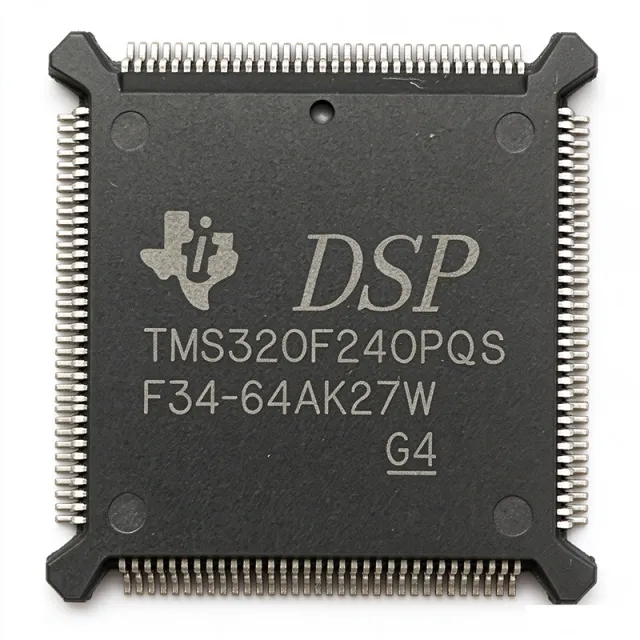
TMS320F240PQS - 20MHz 16-Bit Flash DSP | Texas Instruments
The Texas Instruments TMS320F240PQS is a 16-bit fixed-point digital signal processor and digital signal controller with a 20 MHz clock, 32 KB of flash program memory, and a 132-pin BQFP package measuring 24.13 mm by 24.13 mm. It belongs to the TMS320C2xx generation of DSPs and is optimized for digital motor and motion-control applications. The verified distributor listing identifies the device as a C2xx, C2000-series, 24x-family controller with 16K x 16 words of on-chip flash. A digital signal processor is a specialized microprocessor architecture designed to execute mathematical and control algorithms efficiently. A DSP controller extends that processing capability with embedded memory, digital I/O, timers, analog interfaces, and control-oriented peripherals. The TMS320F240PQS sits in the hierarchy of digital signal controller, fixed-point DSP, microcontroller, embedded processor, and semiconductor. It is intended for systems requiring deterministic real-time control rather than general-purpose computing. The most prominent verified specifications are the 20 MHz operating frequency, 16-bit processor architecture, 32 KB of flash memory, 132-pin BQFP package, and 5 V operating supply identified in the component-comparison data. Its flash memory allows control firmware to be stored directly on the controller. The large 132-pin package exposes the device's extensive motor-control peripheral set, while its 20 MHz clock supports processing associated with the verified 20 MIPS performance figure. The TMS320F240 architecture uses the C2xLP core CPU for fixed-point signal and control processing. Its combination of flash program memory and dedicated real-time peripherals distinguishes it from earlier RAM-programmed DSP controllers. This makes the part relevant to closed-loop motor systems, where acquisition, filtering, transformation, modulation, and actuator calculations must occur within a predictable control interval. The verified family description specifically identifies digital motor and motion control as the optimization target. Typical uses include digital motor control, industrial automation, power-converter control, servo systems, and embedded signal-processing equipment. In such systems, the controller can execute control algorithms while its communication and timing peripherals coordinate external sensors, power stages, and protection functions. The 132-pin BQFP package is appropriate for through-hole industrial or legacy control boards where a large pin count simplifies access to numerous control and communications signals. Designers should verify the complete pinout, timing, peripheral configuration, and electrical limits against the manufacturer datasheet before laying out a new PCB. The verified data does not expose a complete machine-readable 132-pin assignment, so no pin names are inferred here. The 132-pin BQFP package also requires careful lead clearance, solder-joint inspection, and consideration of thermal performance when the controller is mounted alongside power-conversion circuitry. This product record combines verified distributor specifications, source links, package information, lifecycle context, and application-oriented engineering guidance. It distinguishes documented facts from missing data and avoids presenting unverified pin assignments, prices, compliance declarations, or substitute parts as established facts.

TMS320F241FN - 16-Bit 20MHz Flash DSP | Texas Instruments
The Texas Instruments TMS320F241FN is a 16-bit fixed-point digital signal processor and microcontroller with a 20 MHz clock, 16 KB of flash program memory, and a 68-pin PLCC package measuring 24.23 mm by 24.23 mm. It belongs to the TMS320C2xx family and uses the TMS320C2xx core, providing source-code compatibility with TMS320C25 and object compatibility with the TMS320C2xx family. A digital signal processor is a specialized microprocessor architecture optimized for filtering, signal transformation, control, and other mathematically intensive real-time operations. The TMS320F241FN sits within the broader hierarchy of fixed-point DSP controller, digital signal processor, embedded processor, and microcontroller. Its dedicated architecture allows control and signal-processing tasks to be executed without relying on a general-purpose host processor. Key device characteristics include a 16-bit instruction width, 20 MHz operating frequency, and 16 KB of organized flash memory described by the distributor listing as 8K x 16. The verified product description also identifies a 5 V fixed-point DSP architecture, high-performance static CMOS technology, and a 50 ns instruction-cycle time for commercial and industrial grades. The integrated flash memory supports standalone control-system implementations without requiring a separate external program-memory device. The architecture follows the TMS320C2xx execution model and is designed for embedded real-time signal processing. Compatibility with TMS320C25 source code allows qualified legacy algorithms to be migrated without a complete software rewrite, while TMS320C2xx object compatibility supports established software-component reuse. This combination makes the TMS320F241FN relevant to industrial motor control, digital power conversion, instrumentation, and embedded control systems. Typical applications include digital motor control, industrial automation, power-supply control, communications signal processing, and measurement equipment. The 20 MHz processor rate and fixed-point architecture are particularly useful when deterministic execution, compact control loops, and direct access to embedded peripherals are more important than high-level processor performance. Designers should verify the complete electrical limits, peripheral configuration, memory map, and pin assignments against the manufacturer datasheet before schematic capture. PLCC assembly also requires attention to thermal performance, board cleanliness, and socket or soldering process. The distributor data does not provide current unit pricing, inventory quantities, or lead times, so procurement planning should use a current authorized-distributor quotation rather than assumed values. This product record consolidates the verified distributor identity, package, memory, clock, and source links while clearly separating unknown electrical and lifecycle details. It also documents why candidate parts that use a different package or a different processor architecture are not presented as drop-in replacements.