المنتجات (38,000+)

TS507ID - Low-Offset Rail-to-Rail Op Amp | STMicroelectronics
TS507ID

TS507ID - Low-Offset Rail-to-Rail Op Amp | STMicroelectronics

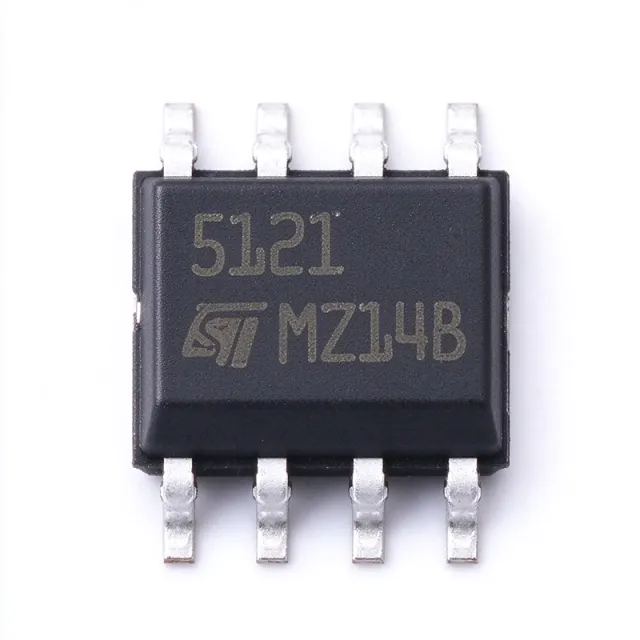
The STMicroelectronics TS507ID is a single-circuit, general-purpose operational amplifier in an 8-pin SOIC package. It is designed around rail-to-rail input and output operation, allowing the amplifier to operate close to the supply rails in precision analog signal chains. The TS507 uses a new trimming technique that produces very low offset voltage without requiring external zeroing, reducing assembly time and eliminating the need for a trim potentiometer in precision measurement circuits. A rail-to-rail operational amplifier is an amplifier whose input common-mode range and output swing extend close to both supply-voltage limits. This capability is valuable when the signal being amplified operates near a positive or negative rail and a conventional amplifier would saturate. The TS507 therefore suits precision instrumentation, sensor interfaces, low-level signal conditioning, and measurement systems where usable signal range is more important than absolute isolation from the rails. The TS507ID is identified by DigiKey and Mouser as a standard, general-purpose instrumentation amplifier section in an 8-SOIC package. Its trimmed internal design targets stable electrical characteristics across the operating range and very low offset without external adjustment. For designs requiring tighter control of input bias current, offset drift, noise, bandwidth, supply current, or temperature range, consult the manufacturer datasheet and select the appropriate TS507 grade and package variant. Because the TS507ID accepts both positive and negative signal inputs and supports near-rail output swing, it can serve as the active element in difference amplifiers, current-to-voltage converters, bridge-sensor front ends, and precision feedback networks. The 8-pin SOIC footprint also allows it to be placed in the same general layout class as many standard single op amps, although engineers should verify the actual pin assignment and stability requirements before substituting another device. When designing with the TS507ID, begin by defining the signal amplitude, common-mode range, required output swing, source impedance, and noise gain. Check the datasheet for the operating voltage range, unity-gain bandwidth, slew rate, input bias current, offset voltage, noise density, and stability conditions. Place the feedback components close to the amplifier, keep sensitive input nodes away from switching-current paths, and use a ground layout that minimizes voltage drops across analog return currents. This page combines manufacturer-level product information, verified distributor listings, package and pin-assignment guidance, application analysis, and drop-in replacement guidance. It also distinguishes confirmed package-compatible TS507 family variants from options that require additional electrical verification, helping engineers narrow a redesign quickly before committing a new component to a PCB.

طلب عرض سعر اتصل بنا
TS512ID - 3 MHz Precision Dual Op Amp | STMicroelectronics
TS512ID

TS512ID - 3 MHz Precision Dual Op Amp | STMicroelectronics

The STMicroelectronics TS512ID is a precision dual operational amplifier with two independent amplifiers, a 3 MHz gain-bandwidth product, and a maximum input offset voltage of 500 µV. The device is supplied in an 8-pin SOIC package and operates from single or dual power supplies, making it suitable for signal-conditioning and instrumentation applications requiring two amplifiers in one package. An operational amplifier is an analog integrated circuit that uses very high open-loop gain to amplify the difference between its inverting and non-inverting inputs. Precision operational amplifiers are a subtype of voltage-feedback amplifiers characterized by low offset voltage, low distortion, low noise, and stable operation with feedback. The dual-amplifier configuration places two amplifiers in one package, reducing board area and simplifying paired signal-processing circuits. The TS512 family provides a 3 MHz gain-bandwidth product, low input offset voltage of 500 µV maximum, low power consumption, short-circuit protection, low distortion, low noise, high channel separation, and internal ESD protection. According to the STMicroelectronics family datasheet, the minimum slew rate is 0.8 V/µs for TS512 and TS512A. The related TS512B has a guaranteed higher minimum slew rate of 1.072 V/µs. The TS512 family uses internal frequency and phase compensation to support stable operation in voltage-follower configurations. This is useful in application circuits where one amplifier buffers a source and the other performs gain or filtering. Its dual supply range is ±1.5 V to ±15 V, while single-supply operation is supported from 3 V to 30 V, allowing use in both conventional analog circuits and higher-voltage industrial interfaces. Typical uses include sensor-signal conditioning, low-level instrumentation, active filtering, audio preamplification, and general analog signal processing. The dual channel can implement matched buffer, gain, summing, or differential stages. Because offset voltage influences accuracy near the zero-voltage operating point, input-source resistance and bias-current compensation should be evaluated carefully. PCB layout should keep input and feedback paths short and place input compensation or filtering components close to the relevant amplifier pins. Both channels should share stable supply decoupling, while avoiding current paths through analog ground that carry output or digital return current. The SOIC package is suitable for conventional surface-mount assembly and conventional thermal design at low to moderate output current. This page consolidates the verified manufacturer-family information, distributor listing details, package data, sourcing information, and engineering guidance for TS512ID. It distinguishes documented TS512-family characteristics from unavailable detailed electrical limits and clearly identifies uncertainty where the supplied source data does not provide a defensible value.

USD $0.43 متوفر
TS512IN - 3MHz Dual Precision Op Amp | STMicroelectronics
TS512IN

TS512IN - 3MHz Dual Precision Op Amp | STMicroelectronics

The STMicroelectronics TS512IN is a precision dual operational amplifier with a 3 MHz gain-bandwidth product, 1.5 V/µs slew rate, and a maximum input offset voltage of 500 µV, supplied in an 8-pin Mini DIP package. It is designed for general-purpose instrumentation, analog signal conditioning, and dual-channel measurement applications where two amplifiers share the same package. A dual operational amplifier is an analog integrated circuit containing two independent amplifier channels. Operational amplifiers are voltage amplifiers whose behavior depends mainly on external feedback components. The TS512IN combines frequency-compensated amplifiers for stable voltage-follower operation, low distortion, low noise, short-circuit protection, and internal ESD protection. The 3 MHz gain-bandwidth product supports useful closed-loop bandwidth well below 3 MHz at higher noise gains, while the 1.5 V/µs slew rate improves response to larger transient signals. A maximum offset voltage of 500 µV helps reduce DC error in precision feedback networks. Its dual-channel organization reduces package count and simplifies PCB routing when two amplified signals must be processed under shared supply conditions. The device operates from single 6 V to dual ±15 V supplies, matching conventional analog and industrial voltage ranges. Internal phase compensation allows voltage-follower use without an external compensation network. Short-circuit protection limits the effects of output overload, although sustained shorts still require appropriate supply and thermal checks. Internal ESD protection improves handling robustness without eliminating the need for normal assembly precautions. TS512IN applications include sensor-interface amplification, low-frequency instrumentation, dual audio-channel control, buffering, active filtering, and general analog signal conditioning. Designers should place input and feedback components close to their associated pins, observe the specified common-mode and output-current limits, and avoid excessive loading near the bandwidth and slew-rate limits. This product page combines verified manufacturer-linked specifications, source URLs, package information, application guidance, and honest comparison limitations. It distinguishes confirmed TS512IN attributes from parameters that require verification before a PCB or production cross-reference is approved.

طلب عرض سعر اتصل بنا
TS514ID - High-Speed Precision Quad Op Amp | STMicroelectronics
TS514ID

TS514ID - High-Speed Precision Quad Op Amp | STMicroelectronics

STMicroelectronics TS514ID is a high-speed, precision quad operational amplifier with four amplifier circuits, internally compensated frequency and phase response, short-circuit protection, internal ESD protection, and a 14-pin SOIC package. The verified product data identifies a maximum offset voltage of 500 uV and highlights a high gain-bandwidth product, low distortion, low noise, low power consumption, and high channel separation. The TS514ID is intended for instrumentation and general-purpose precision signal-processing designs requiring four amplifiers in one package. An operational amplifier, commonly called an op amp, is a voltage-controlled differential amplifier with very high open-loop gain. Its external feedback network determines the closed-loop behavior. The TS514 belongs to the operational-amplifier hierarchy, which includes instrumentation amplifiers, buffer amplifiers, comparators, and general-purpose voltage amplifiers. Internal phase compensation allows the TS514 to operate as a voltage follower despite its high gain-bandwidth product, reducing the external compensation effort required in many designs. The quad architecture integrates four amplifier channels into one 14-pin SOIC-14 package. Verified manufacturer-related product descriptions identify low offset voltage, low power consumption, short-circuit protection, low distortion, low noise, high gain-bandwidth product, high channel separation, and internal ESD protection. These characteristics make the device applicable to precision buffering, signal conditioning, instrumentation, industrial measurement, and general analog signal-processing systems. Each amplifier requires stable supply decoupling and careful handling of output-current limits. The TS514 uses internal frequency and phase compensation. This architecture is particularly useful in follower and precision-gain configurations because the compensation is already incorporated into the device. Its high speed does not eliminate the need for short feedback traces, adequate grounding, and supply bypassing. Designers should avoid long output routing and place input, output, and ground returns so that parasitic capacitance does not degrade stability or transient response. Typical uses include four-channel sensor conditioning, low-level signal amplification, active filtering, voltage buffering, and instrumentation chains requiring several matched amplifier functions. Industrial control and test equipment can also use the quad package to reduce board area compared with four discrete single-amplifier packages. Where precision offset and noise dominate, the complete manufacturer datasheet should be consulted for test conditions and application-specific limits. The principal design trade-off is speed versus power and stability margin. Although the TS514 supports high-speed operation and voltage-follower use, board layout, capacitive loading, output-current demand, and supply bypassing remain critical. A short, low-inductance layout with local decoupling is recommended. Application notes and the manufacturer datasheet should control the final compensation, grounding, and thermal implementation. This product page combines verified distributor and datasheet information with practical guidance on precision analog design, package reuse, selection criteria, and drop-in alternatives. It also distinguishes confirmed TS514-family candidates from cross-package or merely functional substitutes so engineers can avoid redesigns that require PCB changes.

طلب عرض سعر اتصل بنا
TS514IN - Quad Precision Op Amp | STMicroelectronics | DIP-14
TS514IN

TS514IN - Quad Precision Op Amp | STMicroelectronics | DIP-14

The STMicroelectronics TS514IN is a high-performance quad operational amplifier with internal frequency and phase compensation, supplied in a 14-DIP package. The device contains four amplifier channels in one package and is designed for general-purpose instrumentation, signal-conditioning, and analog control applications where stable voltage-follower operation is useful. The verified manufacturer description identifies low offset voltage, low power consumption, short-circuit protection, low distortion, low noise, high gain-bandwidth product, high channel separation, and internal ESD protection as key features. An operational amplifier is an analog integrated circuit that amplifies the voltage difference between its inverting and non-inverting inputs. A quad operational amplifier extends this architecture to four independent channels in one package, reducing board area and simplifying multi-channel designs. The TS514IN belongs to the broader operational-amplifier, analog-amplifier, signal-conditioning, and semiconductor hierarchy. The TS514IN's compensated architecture is intended to support stable operation as a voltage follower despite its high gain-bandwidth product. Internal compensation simplifies circuit design when unity-gain stability is required, while short-circuit protection improves robustness in conventional analog signal paths. Low offset voltage supports precision-oriented instrumentation, and low noise and low distortion are useful for audio and measurement front ends. Four channels make the device suitable for sensor signal conditioning, current-voltage conversion, active filtering, waveform shaping, instrumentation amplifiers, feedback networks, and general analog control loops. The 14-DIP package is appropriate for through-hole prototyping, educational systems, laboratory instruments, and industrial assemblies where a dual-inline footprint is preferred over a fine-pitch surface-mount package. The principal design consideration is to verify the supply-voltage limits, input common-mode range, output swing, input bias current, noise density, and load-current behavior against the manufacturer datasheet before finalizing a new design. Decoupling capacitors should be placed close to the supply pins, and unused amplifier inputs should be tied to a defined voltage within the input common-mode range. This page consolidates the verified manufacturer and distributor information, package details, application guidance, technical limitations, and drop-in replacement analysis. It also identifies parameters that require confirmation from the complete TS514 datasheet rather than substituting unverified assumptions.

طلب عرض سعر اتصل بنا
TS522ID - Dual 15MHz Low-Noise Op Amp | STMicroelectronics
TS522ID

TS522ID - Dual 15MHz Low-Noise Op Amp | STMicroelectronics

The STMicroelectronics TS522ID is a monolithic dual operational amplifier optimized for precision audio signal processing. It provides two amplifiers, a 15 MHz gain-bandwidth product, a 7 V/µs slew rate, low-voltage noise of 4.5 nV/√Hz, and a maximum input offset voltage of 850 µV in an 8-pin SOIC package. The device operates from 5 V to 30 V over an industrial temperature range of -40°C to +125°C. An operational amplifier is a voltage-controlled differential amplifier that uses feedback to amplify the difference between two input voltages. The dual configuration places two amplifiers in one package, allowing stereo audio, balanced signal paths, active filtering, or independent measurement channels to share a common footprint. Within the broader semiconductor hierarchy, the TS522 belongs to the operational-amplifier family, the analog amplifier category, and the signal-conditioning IC hierarchy. The TS522 combines low input offset, low voltage noise, and high dynamic performance for audio-oriented designs. Its 850 µV maximum input offset voltage supports accurate signal amplification, while the 4.5 nV/√Hz voltage-noise density is particularly relevant when processing low-level microphone, musical-instrument, or line-level signals. A 15 MHz gain-bandwidth product provides useful bandwidth for audio and general-purpose precision applications, and the 7 V/µs slew rate improves large-signal response. Internally, each amplifier is configured around high-gain stages with internal ESD protection. The manufacturer datasheet reports low distortion of 0.002%, macromodel inclusion, and excellent frequency stability. These characteristics make the TS522 suitable for precision audio signal chains where low noise, low distortion, and predictable frequency response matter more than very low power consumption. Typical uses include stereo audio preamplification, active crossover filters, mixer input stages, microphone preamplifiers, audio buffer circuits, and low-level sensor-conditioning channels. Two amplifiers in the same 8-pin SOIC package can reduce board area in stereo designs, while the industrial temperature range supports industrial control, communications, and instrumentation equipment. Designers should verify the required supply headroom, input common-mode range, output swing, noise gain, and stability for the selected feedback network. Decoupling capacitors should be placed close to the supply pins, and sensitive audio inputs should use short traces with suitable grounding to minimize parasitic pickup. A SPICE macromodel is available for circuit simulation, but board-level stability and distortion should still be verified with real components. This page consolidates the verified TS522ID operating characteristics, sourcing links, application guidance, design cautions, and replacement information. It also distinguishes confirmed technical facts from parameters that were not present in the supplied source data, helping engineers make a defensible design decision without treating unverified values as guaranteed specifications.

طلب عرض سعر اتصل بنا
TS522IN - 15MHz Dual Low-Noise Op Amp | STMicroelectronics
TS522IN

TS522IN - 15MHz Dual Low-Noise Op Amp | STMicroelectronics

The STMicroelectronics TS522IN is a monolithic dual precision operational amplifier primarily intended for audio applications. Each amplifier provides a 15 MHz gain-bandwidth product, a 7 V/us slew rate, and low voltage noise of 4.5 nV/sqrt(Hz). The device is offered in an 8-pin mini-DIP package for through-hole PCB assembly. An operational amplifier is an analog signal-conditioning IC that uses high open-loop gain and negative feedback to amplify, buffer, filter, or compare small voltage signals. The TS522 belongs to the operational-amplifier hierarchy within linear and amplifier ICs. Its dual-channel architecture integrates two amplifiers in one package, reducing board area and simplifying dual audio-path or differential-signal designs. The TS522IN emphasizes low-noise signal handling, low input offset voltage, and high dynamic performance. Manufacturer descriptions identify a maximum input offset voltage of 850 uV, voltage noise of 4.5 nV/sqrt(Hz), gain-bandwidth product of 15 MHz, and slew rate of 7 V/us. The device also includes internal ESD protection rated at 2 kV and a macromodel for simulation. These characteristics make it relevant to audio preamplification, active filtering, buffering, and general low-noise analog signal chains. The dual amplifier can process two related signals independently, including left and right audio channels or the positive and negative sides of a differential circuit. Its 15 MHz bandwidth provides useful bandwidth for audio and wider-band analog stages, while the 7 V/us slew rate supports rapidly changing waveforms. The 4.5 nV/sqrt(Hz) voltage-noise figure helps reduce amplifier-added noise in high-gain stages, making the TS522IN most useful when the signal source impedance, resistor selection, and feedback topology are controlled carefully. Typical applications include stereo audio preamplifiers, microphone preamplifiers, active low-pass filters, audio buffers, sensor-conditioning stages, and small-signal audio-driver interfaces. The mini-DIP package is appropriate for legacy through-hole designs, test equipment, prototypes, and applications where hand insertion or socket assembly is preferred. Surface-mount production should use an electrically and mechanically verified SO-8-family option rather than assuming the DIP package is interchangeable. When designing around the TS522IN, begin with the power-supply limits and common-mode input range listed in the manufacturer datasheet. Confirm that source and sink output-current requirements remain within the operating limits at the selected gain and load. Place input and feedback components close to the device, maintain a stable ground reference, and use appropriate bypassing at each supply pin. Decoupling capacitors should be placed at the amplifier pins rather than at a distant power entry point. This page consolidates the TS522IN technical characteristics, package constraints, sourcing guidance, application fit, and verified cross-reference information. It also distinguishes documented device attributes from parameters that require confirmation in the manufacturer datasheet, helping engineers assess the part before PCB and production decisions.

طلب عرض سعر اتصل بنا
TS524ID - Quad Low-Noise Audio Op Amp, 15MHz, SOIC-14 | STMicroelectronics
TS524ID

TS524ID - Quad Low-Noise Audio Op Amp, 15MHz, SOIC-14 | STMicroelectronics

The STMicroelectronics TS524ID is a monolithic quad operational amplifier for precision audio signal paths, integrating four low-noise, high-fidelity amplifiers on one silicon die in a 14-pin SOIC (SO-14) surface-mount package. It combines a 15 MHz gain-bandwidth product, a 7 V/µs slew rate and 4.5 nV/√Hz input voltage noise with an input offset voltage of 950 µV maximum and total harmonic distortion of 0.002%. An operational amplifier, or op amp, is a high-gain differential amplifier with two inputs and one output that is used to amplify small signals faithfully across a wide frequency range. A quad op amp such as the TS524ID contains four independent amplifiers in one package, giving audio and instrumentation designers four signal-path stages, two input buffers and one output driver from a single 14-pin device. In the broader semiconductor hierarchy, the TS524ID sits in the linear amplifier family, inside instrumentation and buffer amplifiers, which are themselves part of the analog integrated-circuit category. Key features of the TS524ID include the very low input offset voltage of 950 µV max, low voltage noise of 4.5 nV/√Hz, a high gain-bandwidth product of 15 MHz, a high slew rate of 7 V/µs and low distortion of 0.002%. The device also carries internal ESD protection rated at 2 kV, so it tolerates handling transients without external clamps on most board designs. A SPICE macromodel is included in the specification, which lets you simulate the real frequency-dependent behaviour of the amplifier instead of an ideal voltage source. Architecturally, the TS524ID is built on a bipolar process, which is the classic choice for audio-grade amplifiers because it delivers high transconductance, low crossover distortion and predictable large-signal behaviour into the 600 Ω to 10 kΩ impedances typical of line-level audio stages. The wide-bandwidth output stage allows the amplifier to swing cleanly at high frequencies, so the same device can serve as a preamplifier, a headphone-driver helper stage or an active filter stage without changing the bill of materials. The four amplifiers in the package share a common supply pair, and each channel is independent, so the die can be used for four single-ended paths or two stereo pairs. Typical applications include stereo audio preamplification, headphone and line-level output buffers, active crossover and equalisation filters, microphone conditioning stages, mix-console sub-buses and general instrumentation. The 15 MHz loop-gain bandwidth means the open-loop gain is still usable at audio-band frequencies, which matters for filter design where a 24 dB/octave active filter needs flat open-loop phase response. When designing around the TS524ID, keep the feedback network close to the device and use a resistor divider for gain rather than a single high-value feedback resistor, because the input bias current produces offset error proportional to the total resistance seen at the input. Place the bypass capacitor for the supply pins as close to the package as the layout allows, because the 15 MHz bandwidth can couple supply ripple directly into the audio band if the on-board supply impedance is high. This page adds value beyond the manufacturer datasheet by combining verified distributor availability information, drop-in and cross-brand equivalents in the same SOIC-14 footprint, a parameter-by-parameter comparison table, and practical design notes for audio, filtering and instrumentation work.

طلب عرض سعر اتصل بنا
TS524IN - Quad Low-Noise Precision Op Amp | STMicroelectronics
TS524IN

TS524IN - Quad Low-Noise Precision Op Amp | STMicroelectronics

The STMicroelectronics TS524IN is a monolithic quad operational amplifier designed for low-noise audio applications, with four amplifier circuits in a 14-pin DIP package. Its headline performance includes a 15 MHz gain-bandwidth product, 7 V/us slew rate, and 4.5 nV/sqrt(Hz) input-voltage-noise density. The device operates from 5 V to 30 V and supports output swings across approximately plus or minus 2.5 V to plus or minus 15 V. An operational amplifier is an analog integrated circuit that uses high-gain differential amplification to improve signals applied to its two inputs. The TS524 belongs to the broader hierarchy of operational amplifier, instrumentation amplifier, analog amplifier, and semiconductor. Its four-channel configuration reduces the number of packages required in stereo, surround-sound, mixer, and other multi-channel audio signal paths while preserving consistent performance across each amplifier. Key characteristics include very low input-offset voltage, 4.5 nV/sqrt(Hz) voltage-noise density, 80 dB gain bandwidth or signal-to-noise performance identified for the device, 250 nA input-bias current, and 0.8 uA input-bias current figure listed for the family. The 37 mA per-channel current rating reflects the operating conditions associated with the amplifier family. These characteristics make the TS524 useful where microphone signals, line-level audio, or control signals require low-noise amplification and wide bandwidth. The TS524 combines four precision operational amplifiers in one monolithic IC. Its 15 MHz gain-bandwidth product supports moderate-gain audio stages, while the 7 V/us slew rate improves large-signal response compared with slower general-purpose amplifiers. The low 4.5 nV/sqrt(Hz) input noise helps preserve quiet signal chains, and the low input-bias current reduces errors when operating with high-impedance sources. Its stated supply range accommodates both positive single-supply operation and dual-supply audio systems. Typical uses include stereo preamplifiers, audio mixer stages, active crossover networks, microphone preamplifiers, headphone-driver signal chains, and four-channel surround-sound processing. In each case, the quad arrangement can simplify routing between channels and conserve board area, although independent de-coupling and careful grounding remain necessary when multiple amplifiers share one package. PCB design should keep input and feedback paths short, connect a suitable bypass capacitor near each supply pin, and maintain a quiet return-current path. Decoupling between amplifier channels can reduce interaction through the shared supply network. Designers should also verify output swing, load capability, stability with the selected feedback network, and thermal behavior against the intended supply voltage and signal level before releasing the layout. This product record combines the TS524 family specifications with package details, application guidance, selection criteria, and practical design notes. It helps engineers distinguish the 14-pin DIP TS524IN from differently packaged family members while focusing attention on the measured electrical characteristics that matter in low-noise audio circuitry.

طلب عرض سعر اتصل بنا
TS555CD - 2.7MHz CMOS Timer | STMicroelectronics | SOIC-8
TS555CD

TS555CD - 2.7MHz CMOS Timer | STMicroelectronics | SOIC-8

STMicroelectronics TS555CD is a single CMOS 555-type timer/oscillator operating from 2 V to 16 V, with a maximum frequency of 2.7 MHz and typical supply current of 100 µA at VCC = 5 V. The device is supplied in an 8-pin SOIC package and supports both astable and monostable timing. Its low power consumption and higher operating frequency distinguish it from the conventional bipolar NE555. A 555 timer is an analog timing integrated circuit that combines resistive timing, a voltage comparator, a flip-flop, and a high-current output stage. Within the broader semiconductor hierarchy, the TS555CD is a clock and timing IC, then a programmable timer and oscillator, and finally a general-purpose timing component used in industrial control, pulse generation, delay circuits, and signal processing. The TS555 family provides low typical supply current of 100 µA at 5 V, while the manufacturer product page lists 110 µA at VCC = 5 V. Its maximum astable frequency is 2.7 MHz, compared with 0.1 MHz for the conventional NE555. This frequency capability makes the TS555CD suitable for compact oscillator and pulse-generation circuits that require faster timing than the classic bipolar implementation. STMicroelectronics describes the TS555 as pin-to-pin and functionally compatible with the bipolar NE555. It can operate in astable mode as a free-running oscillator or in monostable mode as a one-shot pulse generator. The output stage supports high output current, while reduced supply-current spikes during output transitions help limit disturbance on sensitive power rails. Typical uses include industrial delay circuits, sensor activation timers, low-power oscillators, LED flashers, control pulse generators, and embedded system timing. Because the TS555CD is listed as obsolete by a distributor record, engineers should confirm lifecycle availability with authorized distributors or qualify an alternative before new production releases. Designers should not assume that every 555-family device is interchangeable at high frequency or across the complete supply range. Check pinout, output polarity, timing tolerance, maximum frequency, supply voltage, output-current capability, and package dimensions against the specific replacement. Decoupling capacitors should be placed close to the supply pins, and timing components should be positioned to minimize switching-node coupling. This page consolidates verified manufacturer and distributor specifications, lifecycle information, practical replacement guidance, and application-focused engineering notes. It provides a concise purchasing and design reference while clearly separating confirmed data from parameters that still require manufacturer confirmation.

طلب عرض سعر اتصل بنا
TS555CN - 2.7MHz Low-Power CMOS Timer | STMicroelectronics
TS555CN

TS555CN - 2.7MHz Low-Power CMOS Timer | STMicroelectronics

The STMicroelectronics TS555CN is a low-power, single CMOS timer with a maximum astable frequency of 2.7 MHz, a typical supply current of 100 µA at 5 V, and an operating supply range up to 18 V, housed in an 8-pin DIP package. It provides the familiar 555 timer functions in astable and monostable configurations while offering pin-to-pin and functional compatibility with the bipolar NE555. A 555 timer is a programmable timing IC that combines a resistor, capacitor, and internal threshold comparator into a compact oscillator or one-shot pulse generator. The TS555CN belongs to the CMOS timer, oscillator, and clock-and-timing hierarchy: it can generate continuous periodic waveforms in astable mode or produce a timed output pulse in monostable mode. Its CMOS implementation is especially useful in low-power and higher-frequency circuits where lower supply current than a conventional bipolar NE555 is valuable. Key features include very low typical supply current, a maximum astable frequency of 2.7 MHz, wide operating voltage support to 18 V, high input impedance, and output compatibility with TTL, CMOS, and logic families. According to the STMicroelectronics manufacturer datasheet, typical supply current is 110 µA at 5 V and 90 µA at 3 V, with reduced current spikes during output transitions. These characteristics make the device practical for portable timing, pulse generation, debouncing, and periodic-control applications. Internally, the TS555CN uses CMOS circuitry to implement the comparator, flip-flop, discharge transistor, and timing-control functions of a standard 555 timer. In astable operation, two external resistors and one capacitor establish the oscillation period; in monostable operation, one resistor and one capacitor set the pulse width. The external timing elements determine practical accuracy, while the timer provides repeatable thresholding and state control. Typical uses include low-power delay circuits, oscillator clocks, LED flashers, pulse generators, debounce networks, and control timing in embedded equipment. The TS555CN can also replace a standard NE555 where the circuit permits CMOS supply current and operating-voltage differences. Before substitution, verify trigger-level, output-drive, timing-tolerance, and maximum-frequency requirements against the actual design. For PCB layout, keep the timing capacitor and resistor leads short, connect the decoupling capacitor close to VCC and GND, and avoid long traces around high-impedance threshold and control pins. Because the DIP package has exposed through-hole leads, mechanical spacing and soldering cleanliness should also be considered. This page combines manufacturer specifications, verified distributor information, replacement guidance, and practical design notes for engineering selection.

طلب عرض سعر اتصل بنا
TS555ID - 2.7MHz Low-Power CMOS Timer | STMicroelectronics
TS555ID

TS555ID - 2.7MHz Low-Power CMOS Timer | STMicroelectronics

The STMicroelectronics TS555ID is a single CMOS 555-type timer and oscillator with a 2.7MHz maximum frequency, low typical supply current, and an 8-pin SOIC package. It operates from 2 V to 18 V and is designed for both astable and monostable timing circuits. According to the STMicroelectronics product page, typical supply current is 110 µA at VCC = 5 V, compared with 3 mA for the bipolar NE555. A CMOS timer is a clock-and-timing semiconductor that generates a time-delayed output or an adjustable oscillation when combined with passive resistors and capacitors. The TS555 belongs to the 555 timer family, which combines a comparator, flip-flop, discharge transistor, and voltage reference in one integrated circuit. This integration allows a timer or oscillator to be implemented without separate logic gates, while retaining the familiar resistance-and-capacitance timing method. The TS555ID provides a maximum astable frequency of 2.7 MHz, substantially higher than the 0.1 MHz maximum cited for the NE555 in the supplied manufacturer data. Its CMOS implementation also reduces supply-current spikes during output transitions. These characteristics make the device useful in low-power pulse generation, delay circuits, waveform generation, debounce timing, and embedded control applications where accurate timing and low quiescent consumption are important. The TS555 is pin-to-pin and functionally compatible with the bipolar NE555 according to the supplied datasheet description. Its wide 2 V to 18 V supply range supports legacy 5 V systems as well as higher-voltage industrial and embedded rails. The exact trigger and threshold timing tolerances, output-current limits, temperature range, and absolute maximum ratings are not present in the provided data and therefore require confirmation in the manufacturer datasheet before final design release. Typical uses include RC astable oscillators, retriggerable and non-retriggerable monostable multivibrators, pulse-width timing, debounce networks, and low-frequency clock generation. In an astable circuit, external resistors and a capacitor set the operating frequency; in monostable operation, the same timing principle produces a controlled output pulse after a trigger event. Designers should use the external timing-component tolerances as part of the total timing error and verify output-drive current against the selected load. Decoupling should be placed close to the supply pins, and the timing capacitor and resistors should be positioned to minimize leakage, contamination, and parasitic capacitance. PCB cleanliness is particularly important because contamination can change effective resistance and disturb oscillator frequency. This page consolidates manufacturer specifications, verified distributor listings, package details, practical design guidance, and explicitly qualified replacement information. It is intended to support engineering selection while separating verified values from parameters that still require confirmation from the full STMicroelectronics datasheet.

طلب عرض سعر اتصل بنا
TS555IN - 2.7 MHz Low-Power CMOS Timer | STMicroelectronics
TS555IN

TS555IN - 2.7 MHz Low-Power CMOS Timer | STMicroelectronics

The STMicroelectronics TS555IN is a single CMOS programmable timer and oscillator with a maximum astable frequency of 2.7 MHz, a 2 V to 16 V supply range, and an 8-pin DIP package. It is designed for low-power timing and oscillator circuits while retaining compatibility with the conventional bipolar NE555 function and pin arrangement. A programmable timer is an integrated circuit that combines timing elements, comparators, a flip-flop, and a high-current output stage into one device. The TS555IN belongs to the 555 timer family, which sits within clock and timing ICs and can operate as a monostable one-shot or an astable free-running oscillator. This integration removes the need for discrete comparator, flip-flop, and discharge-transistor networks in common delay and pulse-generation circuits. The principal advantages are low supply consumption, high operating frequency, and reduced supply-current spikes during output transitions. The cited manufacturer product page reports typical TS555 supply current of 110 uA at a 5 V supply, while a distributor specification listing reports 65 uA under its specified test conditions. The maximum astable frequency of 2.7 MHz is substantially higher than the 0.1 MHz maximum commonly associated with the bipolar NE555 in the supplied comparison data. The TS555IN supports both one-shot and free-running operation. In monostable mode, its output changes state for a controlled interval after an external trigger. In astable mode, external resistors and a capacitor establish repeated output oscillations. The 2 V to 16 V operating range permits use from low-voltage battery-powered equipment through higher-voltage industrial control circuits, subject to the component's detailed absolute maximum ratings. Typical uses include pulse generation, delayed switching, debounce and missing-pulse circuits, simple oscillators, LED flashers, industrial timing modules, and control-signal generation. Its CMOS implementation is particularly useful where standby supply current matters, while its 2.7 MHz maximum frequency supports higher-rate timing than the bipolar reference timer. Designers should preserve the standard 555 interface when making PCB substitutions and should account for the TS555's low-voltage limitations, timing tolerances, and output-drive behavior. Supply bypassing and timing-component placement should follow the manufacturer datasheet, especially in astable circuits operating near the 2.7 MHz upper frequency limit. This product page consolidates manufacturer specifications, distributor availability information, verified cross-reference results, and practical selection guidance. It also distinguishes true same-package replacements from functionally similar timer families that may require different pinouts, voltage tolerances, or application-level qualification.

طلب عرض سعر اتصل بنا
TS556CD - Dual CMOS Timer, 2.7MHz, 14-SOIC | STMicroelectronics
TS556CD

TS556CD - Dual CMOS Timer, 2.7MHz, 14-SOIC | STMicroelectronics

The STMicroelectronics TS556CD is a low-power dual CMOS 555-type timer and oscillator with a maximum frequency of 2.7 MHz, a 2 V to 16 V supply range, and a 14-pin SOIC package. The device combines two independent timer sections, low typical supply current, and pin-to-pin and functional compatibility with the bipolar NE556, making it suitable for precision timing, pulse generation, delay, and oscillator circuits. A 555-type timer is an analog timing integrated circuit that compares an externally controlled voltage with threshold and trigger levels. In monostable mode, it produces one timed output pulse; in astable mode, it oscillates continuously when configured with external resistors and capacitors. The TS556CD uses CMOS circuitry to reduce power consumption while retaining the familiar dual-timer architecture. Key verified features include a maximum astable frequency of 2.7 MHz, low-power operation, and supply current listed in the source data at approximately 130 µA in one distributor summary, while the manufacturer-family description specifies 220 µA typical at VCC = 5 V for TS556. The discrepancy reflects different device variants or source summaries; application designs should verify the exact datasheet value for the ordered part. The 14-SOIC package is suitable for conventional PCB assembly and through-hole-compatible external connections. The TS556CD is useful in pulse-width generation, delay circuits, waveform generation, LED flashing, industrial control timing, low-power signal generation, and embedded control systems. Its dual sections allow two timers in one package when board area is constrained. Because timing accuracy depends on resistor tolerances, capacitor stability, supply variation, and output loading, those components should be selected for the target frequency and temperature range. The principal design consideration is confirming output drive, supply voltage, timing limits, and pin-level compatibility with the surrounding circuit. The manufacturer describes the family as functionally and pin-to-pin compatible with the bipolar NE556, but load conditions and supply-specific timing behavior still require review before substitution. The TS556CD is listed as obsolete by one distributor source, so procurement should confirm lifecycle status and availability before committing to a production design. This page combines the verified TS556CD specifications, sourcing information, lifecycle observations, and application guidance to support design triage. It also highlights why a same-package timer replacement must be checked for frequency, voltage, timing, and output-load compatibility rather than selected by footprint alone.

طلب عرض سعر اتصل بنا
TS556CN - Dual 2.7MHz CMOS Timer | STMicroelectronics
TS556CN

TS556CN - Dual 2.7MHz CMOS Timer | STMicroelectronics

The STMicroelectronics TS556CN is a dual low-power CMOS timer with two independent 555-compatible timing sections, a maximum astable frequency of 2.7 MHz, and a 14-DIP package. Its verified supply-voltage range is 2 V to 16 V, while one secondary result describes the family operating to 18 V; the exact maximum for this orderable device must therefore be confirmed from its datasheet before use. The TS556CN provides 180 µA typical supply current at 3 V and is designed for accurate monostable and astable operation. A CMOS timer is a programmable time-delay and oscillator integrated circuit. It belongs to the timer/oscillator category, within clock and timing ICs and broader semiconductor devices. Each timer section uses external resistors and capacitors to set delay or oscillation behavior, making this device useful where conventional 555-type timing, pulse generation, delay, and repetitive switching are required without a microcontroller. Key verified attributes include dual-timer construction, operation from 2 V to 16 V, a high maximum astable frequency of 2.7 MHz, and pin-to-pin and functional compatibility with bipolar NE556 devices. Reduced supply-current spikes during output transitions can permit lower decoupling capacitance than a conventional bipolar implementation. The stated 180 µA typical current at 3 V supports battery-conscious designs, although load and switching conditions must be checked against the datasheet. The TS556CN uses CMOS circuitry to combine low quiescent consumption with higher timer frequency than the bipolar NE556 comparison cited in the search data. That comparison reports 2.7 MHz maximum frequency for TS556 versus 0.1 MHz for NE556. However, actual operating frequency depends on timing resistors, capacitors, propagation delays, output loading, and supply voltage, so high-frequency layouts require short traces and careful grounding. Typical uses include LED and lamp flashers, pulse generators, delay stages, debounce or retriggerable timing networks, simple oscillators, industrial control timers, and low-power instrumentation. The 14-DIP through-hole package favors prototypes, educational designs, repairable assemblies, and human-built electronics where a socketed or perforated-board implementation is practical. Design with the two timer sections independently unless datasheet pin behavior explicitly permits shared connections. Place timing components close to their associated pins, bypass the supply near the device, and account for output-current limits and threshold tolerances. Because the web evidence provides conflicting voltage-range wording, use the 2 V to 16 V range for this listing and verify absolute maximum and operating limits before releasing production hardware. This page combines verified distributor and datasheet findings, package-aware replacement analysis, and practical timer-circuit guidance. It also distinguishes documented TS556CN data from specifications that were not supplied, avoiding unsupported claims about pricing, lifecycle, compliance, or exact pin assignments.

طلب عرض سعر اتصل بنا
TS556ID - Dual 2.7MHz CMOS Timer | STMicroelectronics
TS556ID

TS556ID - Dual 2.7MHz CMOS Timer | STMicroelectronics

The STMicroelectronics TS556ID is a dual CMOS 555-type timer and oscillator with two independent timing sections, operation from 2 V to 16 V, a maximum astable frequency of 2.7 MHz, and typical supply current of 220 µA at 5 V. It is supplied in a 14-pin SOIC package. The TS556ID combines 555 timer compatibility with CMOS power efficiency and higher timing frequency than the traditional bipolar NE556. A 555-type timer is a programmable clock and timing semiconductor that can operate as a monostable one-shot or astable oscillator. In system hierarchy, the TS556ID belongs to clock and timing ICs, timer ICs, oscillators, and semiconductors. Each internal timer provides resistive and capacitive timing inputs, trigger and reset controls, and an output stage. Two independent sections allow one circuit to generate two events, delays, tones, or periodic waveforms. The verified data identifies the TS556 as a pin-to-pin and functionally compatible bipolar NE556 design, while reducing typical supply current to 220 µA at a 5 V supply. Another source lists 180 µA typical at 3 V. Its 2.7 MHz maximum astable frequency allows shorter timing periods and higher-frequency waveform generation than a 0.1 MHz NE556, subject to the datasheet's timing limits, component tolerances, and output-drive conditions. The TS556ID supports monostable and astable operating modes. In monostable service, an external trigger produces a timed output pulse whose duration is determined primarily by external resistance and capacitance. In astable service, external timing components charge and discharge an internal node, producing continuous oscillation. Engineers should calculate the timing values from the manufacturer datasheet, include realistic resistor and capacitor tolerances, and verify output rise and fall behavior in the intended load. Typical uses include low-power pulse generation, delayed actuator triggering, LED and indicator flashing, audible tones, small signal-clock generation, industrial control timing, and embedded system timing support. The dual architecture is especially useful when two related but nonsynchronous events are needed. Compared with a NE556, the principal benefits are lower typical consumption and a substantially higher maximum astable frequency; NE556 compatibility does not mean every electrical limit is identical. Design with the 2 V to 16 V supply range in mind, especially the output behavior at low supply voltage. Keep the reset and trigger paths free of unwanted noise, select timing-component tolerances for the required frequency accuracy, and provide the bypass and output-loading conditions required by the datasheet. Because timing accuracy depends on real component values and parasitics, breadboard validation is advisable for high-frequency or precision intervals. This page combines verified manufacturer and distributor information, practical timing guidance, and a conservative assessment of drop-in replacements. It distinguishes documented electrical facts from parameters that require datasheet confirmation, helping engineers locate the TS556ID datasheet, evaluate purchasing options, and decide whether a same-package substitute is suitable for an existing PCB.

طلب عرض سعر اتصل بنا
TS556IN - Dual 2.7 MHz CMOS Timer | STMicroelectronics
TS556IN

TS556IN - Dual 2.7 MHz CMOS Timer | STMicroelectronics

The STMicroelectronics TS556IN is a low-power dual CMOS 555-type timer and oscillator with a maximum astable operating frequency of 2.7 MHz, supplied from 2 V to 16 V and packaged in a 14-pin DIP. Each half of the device can operate as a monostable timer, astable oscillator, or frequency divider. The dual timer uses CMOS construction to reduce supply consumption, with one verified source quoting a typical supply current of 100 µA at VCC = 5 V. The TS556 family is also described as pin-to-pin and functionally compatible with the bipolar NE555, which simplifies replacement of legacy timer circuits. A programmable timer is an oscillator-and-triggering circuit that produces a timed output pulse. A 555-type timer belongs to the clock and timing IC hierarchy: timer and oscillator > programmable timer > clock and timing integrated circuit > semiconductor. In monostable mode, one trigger produces a pulse of a defined duration. In astable mode, the two internal comparators and flip-flop repeatedly charge and discharge an external timing capacitor, creating continuous pulses. Two independent timer sections can therefore control separate events or generate related timing sequences. The TS556IN combines several useful characteristics for timer applications. Its maximum astable frequency is 2.7 MHz, allowing short timing periods when supported by suitable external resistors and capacitors. The verified operating-voltage information identifies a 2 V minimum supply and a 16 V maximum supply for TS556IN. Additional family-level features include high output-current capability, reduced supply-current spikes during output transitions, and compatibility with bipolar NE555 implementations. The reported operating-temperature range is -40 °C to +125 °C, supporting industrial-temperature designs. Internally, the TS556 is a CMOS implementation of the classic dual-timer architecture. Each section uses voltage thresholds, a discharge transistor, and an output stage to compare an external capacitor voltage with control levels derived from the supply voltage. CMOS operation is principally valuable for low supply consumption and reduced switching activity compared with the bipolar NE555. Designers must still account for timing-component tolerance, output rise and fall behavior, and the maximum astable frequency when setting high-frequency operating conditions. Typical uses include pulse generation, delay and retrigger circuits, periodic switching, lamp and motor control, low-frequency oscillators, and two-channel industrial timing systems. TS556IN is particularly appropriate where a through-hole 14-DIP footprint and dual timer are required rather than a surface-mount package. In an astable oscillator, external R-A, R-B, and capacitor C values determine the repetition rate and duty cycle; the 2.7 MHz maximum frequency is an important upper-bound constraint for high-speed timing designs. The primary design consideration is preserving the 555-compatible timing architecture while allowing adequate tolerance and ESR for the selected capacitor. Place timing components close to the device, keep discharge-current paths compact, and avoid excessive loading of the threshold and trigger nodes. Because the part is supplied in a through-hole DIP package, board spacing, connector accessibility, and thermal performance should be checked before using it in new compact designs. This product page consolidates verified distributor specifications, manufacturer-family information, application guidance, packaging details, and available replacement references. It distinguishes directly documented TS556IN characteristics from family-level or distributor-supplied information and explicitly identifies data that remains unavailable, allowing engineers to make sourcing and design decisions without relying on unverified assumptions.

طلب عرض سعر اتصل بنا
TS5A2053 - 10Ω SPDT Analog Switch | Texas Instruments
TS5A2053

TS5A2053 - 10Ω SPDT Analog Switch | Texas Instruments

The TS5A2053 is a single-pole double-throw (SPDT) analog switch from Texas Instruments, designed to operate from 1.65 V to 5.5 V. It can handle both digital and analog signals, and signals up to V+ can be transmitted in either direction. The device features a low ON-state resistance of 10Ω (typical) and includes an enable pin for power management. It is available in the 8-pin VSSOP (DCU) package, making it suitable for space-constrained applications. An analog switch is a semiconductor device that selectively connects or disconnects an analog signal path based on a digital control signal. It is a fundamental building block in signal routing, multiplexing, and sample-and-hold circuits. Analog switches are part of the broader category of interface ICs, which manage signal integrity and connectivity between different subsystems in electronic systems. Key features of the TS5A2053 include a low ON-state resistance of 10Ω, which minimizes signal attenuation, and a wide operating voltage range from 1.65 V to 5.5 V, allowing compatibility with various logic levels. The device also offers fast switching speeds, with a typical turn-on time of 20 ns and turn-off time of 15 ns, making it suitable for high-frequency signal routing. The enable pin allows the switch to be disabled, reducing power consumption in standby modes. Technically, the TS5A2053 uses a CMOS process that provides low power consumption and high ESD robustness. The device has a bandwidth of 300 MHz, enabling it to pass high-frequency signals with minimal distortion. The ON-state resistance is flat across the input voltage range, ensuring consistent performance. The device also features break-before-make switching, preventing momentary short circuits between channels. Typical applications include audio signal routing, data acquisition systems, and test equipment. In audio systems, the low ON-state resistance and high bandwidth ensure minimal signal degradation. In data acquisition, the switch can route analog signals to an ADC, with the enable pin allowing power saving when not in use. In test equipment, the TS5A2053 can be used for signal multiplexing and routing. When designing with the TS5A2053, it is important to consider the ON-state resistance and its effect on signal integrity. For high-frequency signals, the parasitic capacitance of the switch can cause signal attenuation, so proper PCB layout and termination are recommended. Additionally, the enable pin should be tied to a defined logic level to avoid floating inputs.

طلب عرض سعر اتصل بنا
TS5A3159QDBVRQ1 - 1Ω SPDT Analog Switch AEC-Q100 | TI
TS5A3159QDBVRQ1

TS5A3159QDBVRQ1 - 1Ω SPDT Analog Switch AEC-Q100 | TI

The Texas Instruments TS5A3159QDBVRQ1 is an automotive-qualified (AEC-Q100) single-pole double-throw (SPDT) 2:1 analog switch with 1Ω typical ON-state resistance (1.3Ω max), operating from a 1.65V to 5.5V supply in a 6-pin SOT-23 (DBV) package. An analog switch is a semiconductor device that routes or gates analog and digital signals under the control of a logic-level input. Within the signal-chain hierarchy, the SPDT analog switch sits in the analog switches and multiplexers family, below large multiplexer arrays and alongside transmission-gate logic. An SPDT device connects one common (COM) terminal to either of two throw terminals (NO or NC), making it the fundamental building block of signal routing and redundancy switching. Key features include break-before-make switching, which prevents momentary channel shorting during transition and eliminates signal distortion when a signal source moves between paths; an excellent total harmonic distortion (THD) specification that preserves audio and precision-signal integrity; and low ON-resistance matching and flatness, which minimize signal error across the input range. The device operates from a single 1.65V to 5.5V supply, compatible with 1.8V, 2.5V, 3.3V, and 5V logic systems. The switch core uses a low-charge-injection MOS transmission-gate architecture with approximately 8pF typical ON capacitance (per TI family data), limiting high-frequency insertion loss in data and RF routing paths. The digital IN pin is logic compatible across the full supply range, and the -Q1 suffix denotes AEC-Q100 qualification with -40C to +125C operation for automotive environments. Typical applications include automotive audio source selection, sensor-signal multiplexing in battery-management and body-control modules, UART/SPI/SMBus line sharing, and general-purpose signal gating in industrial systems. The 2.9mm x 1.6mm SOT-23-6 footprint suits densely populated boards. Design tip: terminate or AC-ground unused throw terminals to reduce crosstalk, and place the device close to the signal source to minimize parasitic trace capacitance. This page synthesizes distributor pricing, drop-in alternatives, comparison tables, and practical design notes not found in the manufacturer datasheet.

USD $0.28 اتصل بنا
TS7003ITD833 - 12-Bit 300ksps SAR ADC, 2.5V Ref, TDFN-8 | Silicon Labs
TS7003ITD833

TS7003ITD833 - 12-Bit 300ksps SAR ADC, 2.5V Ref, TDFN-8 | Silicon Labs

The Silicon Labs TS7003ITD833 is a 12-bit, 300 ksps successive-approximation analog-to-digital converter (ADC) with a single-ended single-channel input, integrated +2.5V reference, and a high-speed serial digital interface, packaged in an 8-pin TDFN (3x3 mm) with exposed pad for thermal and ground integrity. Designed for single-supply operation from +2.7V to +3.6V, it draws less than 1 mA at full 300 ksps conversion rate. An ADC in this product category is a mixed-signal data converter that translates real-world analog voltages into discrete digital codes. The successive-approximation register (SAR) architecture family uses a binary-search algorithm with an internal track-and-hold front end, achieving a balance of speed, accuracy, and low power consumption suitable for embedded sensing, instrumentation, and process-control front-ends. This part sits within the broader hierarchy: ADC -> data converter -> mixed-signal IC -> semiconductor. Its integrated reference removes an external component and reduces board area, an important benefit for compact sensor-interface designs. Key features include 12-bit resolution, 300 ksps throughput, a high-bandwidth input track-and-hold amplifier, and an internal +2.5V reference. The serial interface reduces pin count compared to parallel-output ADCs, simplifying routing and host-MCU connection. Low conversion-mode power consumption and an industrial temperature range support battery-aware and factory-floor deployments alike. The TS7003ITD833 successive-approximation architecture implements a charge-redistribution DAC internally, capturing input samples on the T/H at the rising edge of CNVST and presenting results one frame later through the SPI-compatible serial port. The integrated reference and single-supply rail minimizes external component count, while the 8-pin TDFN EP package provides a low-impedance thermal/ground path that enhances noise immunity at full throughput. Typical applications include industrial process-control analog front-ends, portable battery-powered data loggers, sensor-signal digitizers, weigh-scale and load-cell readouts, and microcontroller-based instrumentation. Use it where channel count is small, sampling rate is moderate, and PCB real estate is at a premium. When designing with this ADC, place the decoupling capacitor directly between AVDD and GND, keep analog and digital ground returns separated until they join at the exposed pad, and respect the tACQ acquisition-time timing parameter when writing firmware. Driving the analog input from a low-impedance buffer maintains data-sheet linearity at high source resistances. This page synthesizes distributor pricing, drop-in alternatives, and practical design notes not found in the manufacturer datasheet to help procurement and design engineers evaluate the TS7003ITD833 for new designs and second-source risk mitigation.

طلب عرض سعر اتصل بنا
TS7221BILT - Single BiCMOS R2R uPower Comparator | STMicroelectronics
TS7221BILT

TS7221BILT - Single BiCMOS R2R uPower Comparator | STMicroelectronics

The STMicroelectronics TS7221BILT is a single BiCMOS rail-to-rail micropower comparator housed in a 5-pin SOT-23 (SOT-23-5) package, designed for space- and weight-critical designs. It is fully specified at 2.7 V, 5 V and 10 V operation, drawing only a few microamperes of supply current while delivering rail-to-rail input performance and an open-drain output stage. The 'B' grade denotes a tighter input offset voltage grade versus the 'A' suffix variant, while the 'I' temperature suffix indicates the -40C to +85C industrial operating range and 'LT' indicates SOT-23-5 tape-and-reel packaging. A comparator is an analog building block that compares two input voltages and produces a logic-level output indicating which is larger. Micropower comparators like the TS7221 occupy a position in the power-management/analog signal-chain hierarchy below op-amps but above simple logic gates, and are favoured for always-on battery-powered designs where quiescent current dominates total energy consumption. Within ST's broader comparator family, the TS7221 sits alongside the TS7222 (dual) and TS7223 (quad) as the single-channel foundation of the series. Key features include rail-to-rail input common-mode range, an open-drain output that allows wired-OR logic and level-shifting to any pull-up voltage, very low supply current typically well under 10 uA, and 5 V/10 V operation suitable for industrial sensor interfaces. The BiCMOS process combines CMOS input stages with bipolar output drive for a balance of low power and reasonable switching speed. Internal ESD protection on the inputs (HBM 2000 V per the datasheet absolute maximum ratings) further improves robustness in handheld and field-deployed equipment. Typical applications include battery-pack voltage monitoring, threshold detectors, window comparators, and signal conditioning in IoT sensor nodes, wearables, and portable medical devices. The small SOT-23-5 footprint also makes the device attractive for space-constrained designs such as hearing aids and remote keyless-entry keyfobs. When designing with this part, choose the pull-up resistor on the open-drain output based on the desired propagation delay versus power budget; lower pull-up resistance speeds up edges but increases static current when the output is LOW.

طلب عرض سعر اتصل بنا
TS902ID - Dual Rail-to-Rail Op Amp with Standby | STMicroelectronics
TS902ID

TS902ID - Dual Rail-to-Rail Op Amp with Standby | STMicroelectronics

The STMicroelectronics TS902ID is a dual rail-to-rail CMOS operational amplifier with a standby position, offering 1.4 MHz gain-bandwidth product, 10 mV offset voltage, and operation from single or dual supplies up to 16 V in a 14-pin SOIC package. The device is intended for instrumentation, industrial control, and signal-conditioning systems where low-power standby operation and rail-to-rail input and output behavior are useful. An operational amplifier is an analog integrated circuit that amplifies the voltage difference between its two inputs while using negative feedback to set the gain. The TS902ID belongs to the operational-amplifier hierarchy, where a dual amplifier provides two amplifier channels in one package. Rail-to-rail input and output stages allow signals to approach the supply rails, while the standby function reduces supply consumption and places the outputs in a high-impedance state. Key features include rail-to-rail input and output voltage ranges, a 1.4 MHz gain-bandwidth product, and 10 mV typical input offset voltage. The amplifier supports single- or dual-supply operation from 2.5 V to 16 V according to the available manufacturer information, and its standby current is specified at 0.5 uA. The 14-SO package supports conventional surface-mount assembly and exposes both amplifier channels and the standby control. The TS902ID uses a CMOS operational-amplifier architecture designed for general-purpose analog signal conditioning. Its low standby current supports portable and instrumented systems that need to reduce consumption when measurements are not active. Rail-to-rail operation is useful when the available signal range is close to the supply voltage, although input common-mode, output swing, noise, and stability conditions still need to be checked against the application. Typical applications include low-power instrumentation, industrial sensor interfaces, battery-operated measurement equipment, audio and control-signal conditioning, and dual-channel analog systems. The dual-channel configuration can reduce board area when two independent signal paths are required. The standby position is particularly appropriate for systems that periodically disable the amplifier while retaining the device in the circuit. When laying out a TS902ID design, keep the input and output paths short, provide stable feedback compensation, and bypass the supply pins with suitable ceramic capacitance. Do not assume that standby mode preserves signal accuracy at the moment of switching; verify the timing against the system requirements. The manufacturer datasheet should be used for the complete electrical limits, pin connections, and application recommendations. This page combines verified manufacturer and distributor references with practical engineering guidance for instrumentation, power-conscious analog design, and drop-in replacement assessment.

طلب عرض سعر اتصل بنا
TS912ID - Dual Rail-to-Rail CMOS Op Amp | STMicroelectronics
TS912ID

TS912ID - Dual Rail-to-Rail CMOS Op Amp | STMicroelectronics

STMicroelectronics TS912ID is a dual rail-to-rail CMOS operational amplifier with two independent amplifiers, an 8-pin SOIC package, and operation from single or dual supplies. Verified distributor listings identify it as a 2.7 V to 16 V device with approximately 800 kHz gain-bandwidth product and 1.3 V/us slew rate. The rail-to-rail input and output architecture supports signal stages whose operating range approaches the available supply voltage. An operational amplifier is an analog building block that uses high open-loop gain to amplify voltage differences while feedback determines the closed-loop behavior. A dual op-amp combines two amplifiers in one package, allowing designers to implement filters, buffers, level conversions, or paired signal-conditioning stages while reducing board area. CMOS construction supports low-power and low-noise signal-chain designs across industrial, instrumentation, communications, and consumer equipment. The TS912ID's rail-to-rail input range includes both supply rails, while its rail-to-rail output can swing close to the upper and lower limits. The verified 800 kHz bandwidth provides useful response for general-purpose low-frequency and moderate-frequency applications, while the 1.3 V/us slew rate supports faster transitions than very low-bandwidth precision amplifiers. Two independent, frequency-compensated amplifiers are contained in the same 8-SOIC package. Supply flexibility is central to the device: it can operate from a single 2.7 V minimum supply or from dual positive and negative rails. This makes it suitable for battery-powered instrumentation, active filtering, transducer interfaces, and general analog signal conditioning. Designers should still verify input and output common-mode limits, output-load behavior, noise, input-bias-current requirements, and stability against the conditions of the manufacturer datasheet. Typical uses include low-frequency active filters, sensor-signal conditioning, audio and communications interface blocks, voltage buffering, and two-channel sensor amplification. The SOIC-8 package is straightforward for conventional PCB assembly and breadboard or prototype layouts, although exposed-pad thermal management is not applicable. The primary design consideration is to place input, feedback, and decoupling components so that high-gain layouts remain stable. Keep sensitive input traces short, maintain a low-impedance ground reference, and follow the datasheet's recommended bypass capacitance. Verify the actual output swing against the load and required logic or sensor levels rather than assuming ideal rail-to-rail behavior. This page combines verified distributor pricing, manufacturer datasheet access, same-package replacement data, and practical selection guidance. It separates explicitly published facts from parameters requiring design verification, helping engineers source TS912ID without relying on generic amplifier descriptions.

طلب عرض سعر اتصل بنا
TS912IN - Dual Rail-to-Rail CMOS Op Amp | STMicroelectronics
TS912IN

TS912IN - Dual Rail-to-Rail CMOS Op Amp | STMicroelectronics

The STMicroelectronics TS912IN is a dual rail-to-rail CMOS operational amplifier with two amplifier channels, a 2.7 V to 16 V supply range, and an 8-pin Mini DIP package. The device supports single-supply or dual-supply operation, with rail-to-rail input and output voltage ranges. According to the manufacturer datasheet, its typical input bias current is only 1 pA, maximum input offset voltage is 2 mV, and supply current is approximately 200 µA per amplifier at a 3 V supply. These characteristics make the TS912IN suitable for low-power instrumentation, sensor interfaces, and signal-conditioning circuits that require low input bias and flexible supply operation. A CMOS operational amplifier is a voltage amplifier whose differential input controls the voltage applied to its output. Rail-to-rail input and output ratings allow the amplifier to operate close to the positive and negative supply rails, increasing the usable output range in single-supply systems. In the electronics hierarchy, the TS912IN is a dual operational amplifier, which belongs to the broader class of analog amplifier ICs and ultimately to integrated circuits used for analog signal processing. Key features include two independent amplifier channels, rail-to-rail input and output operation, and a 2.7 V to 16 V total supply range. The 1 pA typical input bias current is particularly useful for high-impedance sources because it minimizes source-loading error. Maximum input offset voltage of 2 mV supports accurate amplification of signals near the lower end of the input range. Operation from a 3 V supply at approximately 200 µA per amplifier also helps limit power consumption in battery-operated equipment. The TS912IN uses CMOS input circuitry to provide low bias current and low supply consumption. Rail-to-rail input behavior is important when the signal can approach either supply rail, while rail-to-rail output capability allows the output to use much of the available supply voltage. Designers should still account for output-current limits, load impedance, input common-mode behavior, and output-voltage headroom under the selected supply voltage and load conditions. Typical uses include low-power sensor signal conditioning, portable measurement instruments, battery-powered monitoring, and general-purpose analog filtering. The dual configuration allows one package to provide two amplifier channels for gain stages, buffers, comparators, or active filters. When the source impedance is high, the 1 pA typical bias current reduces loading, although PCB leakage and guard-ring techniques may still be necessary in demanding measurements. When designing around the TS912IN, use stable bypass capacitance at the supply pins and keep feedback components close to the amplifier pins to minimize parasitic effects. Confirm the required output swing, load, input range, and noise performance against the manufacturer datasheet before finalizing a high-gain or precision application. This page consolidates the verified manufacturer descriptions, distributor references, package information, technical characteristics, and substitution constraints for the TS912IN. It also distinguishes verified data from unavailable pricing, compliance, and pin-mapping details, helping engineers evaluate the amplifier without treating unverified substitute parts as drop-in equivalents.

طلب عرض سعر اتصل بنا