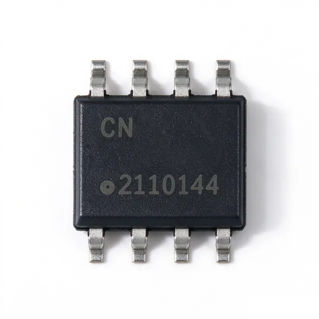
AT91SAM7A2-AU
AT91SAM7A2-AU - 30MHz ROMless ARM7 MCU | Microchip | LQFP
The Microchip Technology AT91SAM7A2-AU is a 16/32-bit ARM7-based ROMless microcontroller operating at up to 30 MHz, with 16 KB of internal RAM, 57 general-purpose I/O lines, and a 176-lead LQFP surface-mount package measuring 24 mm by 24 mm. Its ARM7 RISC architecture, mixed 16/32-bit instruction set, and integrated debug support target embedded control systems requiring deterministic real-time behavior without an embedded boot Flash memory. According to the Microchip documentation, the device also supports 64 KB of internal high-speed Flash organized into 512 pages and includes embedded ICE and Debug Communication Channel support.
An ARM7-based microcontroller is a 32-bit reduced-instruction-set-computing control device whose Thumb instruction mode supports compact 16-bit code while its 32-bit instruction set handles more complex operations. In the product hierarchy, the AT91SAM7A2-AU is a microcontroller, embedded processor, semiconductor, and programmable control component. It sits above general-purpose computing because its peripherals, interrupt structure, and embedded debug interface are tailored to industrial, communications, and real-time equipment.
Principal features include a 30 MHz maximum operating frequency, 16 KB of internal RAM, 57 general-purpose I/O lines, and an integrated 10-bit ADC interface. The device provides PWM channels, USART-based serial communications, and an ARM7TDMI-class RISC core. Its 176-LQFP package exposes substantially more I/O and peripheral connections than small leaded packages, making the device suitable for systems that need broad external connectivity while retaining a conventional leaded package for inspection and assembly.
The ROMless architecture is the most important engineering distinction. Because the AT91SAM7A2-AU does not provide a complete application program in its internal Flash, a boot system must load firmware into external memory before normal execution. This arrangement can separate boot code from the main application, permit controlled recovery or firmware updates, and allow the same microcontroller target to support different storage configurations. System designers must therefore budget for external memory, address-bus correctness, startup code, and sufficient flash endurance for the selected update strategy.
Typical uses include industrial controllers, serial gateways, data acquisition equipment, building-control interfaces, and embedded access systems. The 57 I/O lines support multiple sensors, actuators, communications ports, and status indicators without requiring a companion I/O expander in moderate-complexity designs. The ADC supports analog measurement, while the USART and PWM resources suit sensor monitoring, actuator control, and supervisory communications. The large LQFP footprint is advantageous for prototype accessibility but requires a 176-lead PCB layout and careful consideration of assembly cost.
When designing around this device, verify the external-memory interface, boot configuration, pin multiplexing, and signal levels before committing the PCB. Because the part is ROMless, firmware storage and the boot sequence are part of the system architecture rather than optional software details. A legacy ARM7 design should also include the appropriate debugger, startup routines, clock configuration, and memory timing for the selected external devices.
This product overview combines the exact orderable MPN, package and core details, practical firmware considerations, and qualified replacement guidance for engineers evaluating an obsolete ARM7 control platform. It also distinguishes true drop-in interchangeability from newer Cortex-M devices that may provide similar peripherals but require different firmware, package layouts, and board resources.
طلب عرض سعر
اتصل بنا