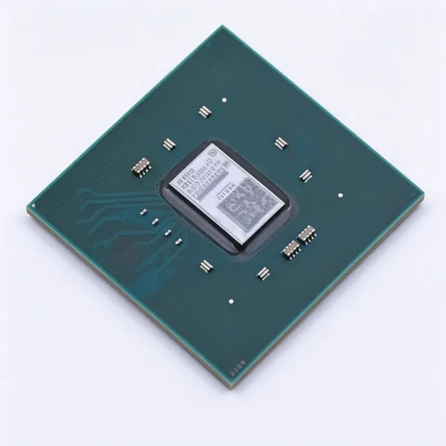
XC7K70T-2FBG484C
XC7K70T-2FBG484C - 65,600-Cell Kintex-7 FPGA | AMD Xilinx
The AMD Xilinx XC7K70T-2FBG484C is a Kintex-7 field-programmable gate array built on 28 nm process technology, with 65,600 programmable logic cells, 285 user I/Os, and a 484-pin FCBGA package. The -2 speed designation targets high-performance designs, while the XC7K70T device family combines programmable logic, DSP processing resources, block RAM, and high-speed serial transceivers in one device. The part is supplied in a tray and is identified by the FBG484 package code, with a 1.00 mm ball pitch and a 23 mm by 23 mm package body.
A field-programmable gate array is a semiconductor device whose digital logic, interconnect, and processing blocks are configured after manufacture. In the product hierarchy, an FPGA belongs to programmable logic devices, then digital programmable logic, and ultimately the broader semiconductor category. Unlike a fixed-function application-specific integrated circuit, an FPGA can be reprogrammed for protocol handling, signal processing, control logic, hardware acceleration, or interface bridging, allowing one physical design to support multiple system functions.
The Kintex-7 architecture provides a balanced combination of logic density, signal processing, memory, and connectivity for communications, industrial, imaging, and embedded systems. Its 65,600 logic cells and 285 user I/Os support complex parallel datapaths and external interfaces. The manufacturer documentation identifies MMCM and PLL resources for clock management, while the 484-ball package provides substantial I/O and power connectivity for high-speed board designs. The -2 performance grade is intended for designs requiring stronger timing performance than the -1 grade.
From a system perspective, the device can combine acquisition logic, filtering, protocol conversion, and interface control without partitioning those functions among multiple fixed chips. This integration reduces component count on boards with limited area and allows firmware or bitstream updates during product development. However, FPGA performance depends on the selected clock speed, I/O standards, memory interface configuration, routing congestion, and whether the design meets timing constraints after placement and routing.
Typical uses include wireless baseband processing, industrial automation, real-time video pipelines, network interface adaptation, test equipment, and custom hardware accelerators. In these systems, the XC7K70T-2FBG484C is valuable when designers need substantial parallel logic, flexible I/O, DSP resources, and field-updateable behavior. Designs requiring deterministic low-latency computation can implement pipelines directly in programmable logic, while clock-management resources support multiple internal and external clock domains.
PCB implementation requires careful power planning and signal-integrity control. The 1.00 mm pitch FCBGA needs a multilayer board with short return paths, appropriate decoupling, and controlled-impedance routing. Designers should follow the AMD package and board-design guidance for ball assignment, power and ground connectivity, thermal management, and high-speed transceiver layout. The dense package also makes assembly, inspection, and rework more demanding than a leaded or coarse-pitch package.
This product summary consolidates the exact ordering information, package characteristics, verified logic and I/O figures, same-package alternatives, comparison parameters, and practical implementation guidance into one engineering-focused reference. It also distinguishes package-identical speed and temperature-grade options, helping designers determine whether a substitute preserves the intended PCB footprint and system timing requirements.
طلب عرض سعر
اتصل بنا