المنتجات (38,000+)

AD9070BR - 10-Bit 100 MSPS ECL ADC | Analog Devices
AD9070BR

AD9070BR - 10-Bit 100 MSPS ECL ADC | Analog Devices

The Analog Devices AD9070BR is a monolithic 10-bit sampling analog-to-digital converter with a 100 MSPS conversion rate, an on-chip track-and-hold circuit, and ECL digital interfaces. It consumes 600 mW typical at 100 MSPS, provides 230 MHz analog input bandwidth, and accepts a 1 V p-p analog input range in a ceramic DIP package. A sampling ADC is a data-conversion IC that samples an analog voltage at a controlled instant and converts that sample into a digital code. The AD9070 belongs to the ADC and DAC product hierarchy, where it functions as a high-speed parallel-output converter. Its 100 MSPS throughput supports wideband signal acquisition while its 230 MHz analog bandwidth allows sampling signals above the converter's Nyquist frequency when used with suitable filtering. The AD9070's primary characteristics include 10-bit resolution, 100 MSPS conversion, 600 mW typical power at 100 MSPS, a 1 V p-p analog input range, and ECL-compatible digital outputs. Its on-chip track-and-hold circuitry reduces the need for external sample-and-hold components. The manufacturer also identifies an on-chip reference and a differential clock input as standard features. This converter combines an on-chip reference with an integrated sampling structure and ECL interface. ECL output levels are suited to high-speed digital systems that require fast data transfer, although the receiving logic, clock distribution, supply arrangement, and termination network must be designed carefully. According to the Analog Devices product page, the AD9070 operates over its full operating range with outstanding dynamic performance. Typical applications include broadband communications test equipment, digital oscilloscope and waveform-analysis front ends, radar or electronic-surveillance signal acquisition, high-speed instrumentation, and communications receivers. The 230 MHz analog bandwidth is especially useful when the input path must preserve high-frequency content, while the 100 MSPS conversion rate determines the maximum real-time sampling bandwidth. The main design consideration is that this is a high-speed, single-supply converter rather than a general-purpose low-voltage ADC. Layout must minimize clock and analog-input ringing, provide suitable input and reference decoupling, and route the 10-bit ECL output with controlled impedance. The exact ceramic-DIP pinout and full application circuit should be checked against the manufacturer datasheet before layout release. This page consolidates verified manufacturer information, distributor availability, pricing, technical comparisons, and engineering guidance. It also distinguishes documented AD9070BR capabilities from unverified substitute and pinout information so that procurement and design decisions can be made without treating inferred data as confirmed specifications.

طلب عرض سعر اتصل بنا
AD9071BR - 10-Bit, 100 MSPS ADC | Analog Devices
AD9071BR

AD9071BR - 10-Bit, 100 MSPS ADC | Analog Devices

Analog Devices AD9071BR is a 10-bit, 100 MSPS monolithic sampling analog-to-digital converter with an on-chip track-and-hold circuit, a 280 MHz analog input bandwidth, and TTL/CMOS-compatible digital outputs in a 28-lead plastic SOIC package. The converter operates from a single 5 V supply and requires an encode clock for full-performance operation. A sampling ADC is an analog-to-digital converter that uses an internal track-and-hold circuit to capture an input voltage before conversion. It belongs to the ADC hierarchy, which forms part of data-converter and signal-processing semiconductors. The AD9071 combines sampling, quantization, an internal reference, and parallel digital output in one device, allowing analog signals to be digitized for subsequent digital processing. The principal features include 10-bit resolution, a maximum conversion rate of 100 MSPS, low power operation at 100 MSPS, an on-chip track-and-hold circuit, and an on-chip reference. The analog input range is 1 V peak-to-peak, while the digital interface supports TTL-compatible 5 V or 3.3 V output operation. Its 280 MHz analog bandwidth is well above the 100 MSPS conversion rate, providing bandwidth for input signals and sampling requirements. The AD9071 uses a parallel digital output architecture rather than a serial interface. This allows captured words to be transferred directly into digital logic, buffers, DSPs, or programmable logic when their timing interfaces are compatible. The 28-lead package provides separate digital data and control connections, but the verified source excerpts supplied for this record do not include a complete pin-number-to-function table. Typical applications include digital communications, signal-intelligence systems, and other high-speed signal-processing installations. The device is particularly relevant where a sampling rate of 100 MSPS, 10-bit resolution, and a 1 V peak-to-peak input range are required without the complexity of a serial-output converter interface. Designers should treat the single 5 V analog supply and the encode clock as central to circuit planning. Input conditioning must provide a suitable 1 V peak-to-peak signal, while clock and digital-interface timing must be controlled to preserve conversion performance. The complete manufacturer datasheet should be used to verify pin functions, input common-mode requirements, output timing, and recommended application circuitry. This page consolidates the verified manufacturer descriptions, available distributor references, package information, selection trade-offs, and practical design guidance for AD9071BR. It also clearly separates confirmed parameters from information that was not supplied, avoiding unsupported electrical or replacement claims.

طلب عرض سعر اتصل بنا
AD9081BBCZ - Quad 16-Bit 12GSPS RF DAC & 12-Bit 4GSPS ADC | Analog Devices
AD9081BBCZ

AD9081BBCZ - Quad 16-Bit 12GSPS RF DAC & 12-Bit 4GSPS ADC | Analog Devices

The AD9081BBCZ is a highly integrated mixed signal front end (MxFE) from Analog Devices, combining a quad, 16-bit, 12 GSPS RF digital-to-analog converter (DAC) core and a quad, 12-bit, 4 GSPS RF analog-to-digital converter (ADC) core. This device is designed for wideband communication systems, radar, and test and measurement applications, offering exceptional dynamic range and bandwidth. The AD9081 features a 16-lane, 24.75 Gbps JESD204C or 15.5 Gbps JESD204B serial interface, enabling high-speed data transfer to FPGAs and ASICs. The device is packaged in a 324-ball BGA-ED (15x15 mm) package, providing excellent thermal and electrical performance. A mixed signal front end (MxFE) is a single-chip solution that integrates high-speed data converters with analog front-end circuitry, such as amplifiers, filters, and mixers, to interface directly with RF signals. In the signal chain hierarchy, the MxFE sits between the antenna and the digital baseband processor, replacing multiple discrete components with a single, highly integrated device. This integration reduces board space, power consumption, and design complexity while improving performance by minimizing parasitic effects and signal degradation. Key features of the AD9081 include a 16-bit DAC with a maximum sample rate of 12 GSPS, a 12-bit ADC with a maximum sample rate of 4 GSPS, and a flexible digital signal processing (DSP) chain with programmable decimation and interpolation filters. The device supports multiple operating modes, including single-band and multi-band configurations, and offers a wide input frequency range up to 5 GHz for the ADC and output frequency range up to 7 GHz for the DAC. The AD9081 also includes an integrated clock multiplier, phase-locked loop (PLL), and digital up/down converters, simplifying system design. The AD9081 utilizes advanced BiCMOS process technology, achieving high linearity and low noise performance. The DAC features a spurious-free dynamic range (SFDR) of [DATA_NEEDED: SFDR] dBc, while the ADC achieves a signal-to-noise ratio (SNR) of [DATA_NEEDED: SNR] dBFS. The device operates from a 1.0 V core supply and 1.8 V I/O supply, with a total power dissipation of [DATA_NEEDED: power dissipation] W. The JESD204C interface supports subclass 1 deterministic latency, ensuring precise synchronization across multiple devices. Typical applications include 5G massive MIMO base stations, phased array radar, electronic warfare, and broadband test and measurement equipment. The AD9081's high sample rates and wide bandwidth make it ideal for direct RF sampling architectures, eliminating the need for multiple downconversion stages. In 5G systems, the device enables the digitization of entire frequency bands, simplifying the radio design and improving flexibility. When designing with the AD9081, careful attention must be paid to power supply decoupling and clock jitter, as these directly impact the converter's dynamic performance. The device requires a clean, low-jitter clock source, and the use of high-quality bypass capacitors is essential. Additionally, the thermal management of the 324-ball BGA package should be considered, as the device can dissipate significant power at high sample rates.

طلب عرض سعر اتصل بنا
AD9172BBCZ - Dual 16-Bit 12.6 GSPS RF DAC | Analog Devices
AD9172BBCZ

AD9172BBCZ - Dual 16-Bit 12.6 GSPS RF DAC | Analog Devices

The AD9172BBCZ is a high-performance, dual, 16-bit digital-to-analog converter (DAC) from Analog Devices, designed for direct-to-RF wireless applications. It supports DAC sample rates up to 12.6 GSPS and features an 8-lane, 15 Gbps JESD204B data input port, an on-chip DAC clock multiplier, and advanced digital signal processing (DSP) capabilities for single-band and multiband signal generation. The device is housed in a 144-ball BGA-ED (10x10 mm) package, offering a compact solution for high-density RF systems. A digital-to-analog converter (DAC) is an electronic component that converts digital data into an analog signal. In RF applications, a high-speed DAC like the AD9172 enables direct synthesis of radio frequency signals, eliminating the need for multiple upconversion stages. This reduces system complexity, power consumption, and board space. The AD9172 belongs to the family of RF DACs, which are specialized data converters optimized for generating signals in the gigahertz frequency range, often used in software-defined radios, radar, and communications infrastructure. Key features of the AD9172 include dual 16-bit DAC cores, a maximum sample rate of 12.6 GSPS, and an integrated JESD204B interface supporting up to 15 Gbps per lane. The on-chip clock multiplier allows flexible clocking from lower-frequency references, simplifying system design. The device also includes digital upconversion (DUC) and channelizer blocks, enabling multiband operation and reducing the digital processing load on FPGAs or ASICs. These features make the AD9172 ideal for applications requiring wide instantaneous bandwidth and high spectral purity. From a technical perspective, the AD9172 leverages advanced CMOS process technology to achieve high-speed operation while maintaining excellent dynamic performance. The DAC architecture includes a current-steering core with integrated output matching, providing a differential output that can drive RF transformers or amplifiers directly. The device supports multiple operating modes, including real and complex output, and offers programmable interpolation filters to optimize signal quality. The JESD204B interface simplifies high-speed data transfer, reducing the number of digital I/O pins compared to parallel interfaces. Typical applications for the AD9172 include wireless base stations, radar systems, electronic warfare, and test and measurement equipment. In wireless infrastructure, the device enables direct RF synthesis for 5G NR and LTE signals, supporting carrier aggregation and MIMO configurations. In radar, the high sample rate and wide bandwidth allow generation of complex waveforms for improved target detection. The device is also suitable for software-defined radio platforms, where flexibility and performance are critical. When designing with the AD9172, careful attention must be paid to power supply decoupling and clock jitter, as these directly impact the output signal quality. The device requires multiple supply rails, and proper filtering is essential to achieve the specified noise and spurious performance. Additionally, the JESD204B interface must be configured correctly to ensure reliable data transfer, and the reference clock should be generated from a low-jitter source to minimize phase noise.

طلب عرض سعر اتصل بنا
AD9173BBCZ - Dual 16-Bit 12.6 GSPS RF DAC | Analog Devices
AD9173BBCZ

AD9173BBCZ - Dual 16-Bit 12.6 GSPS RF DAC | Analog Devices

The AD9173BBCZ is a high-performance, dual, 16-bit digital-to-analog converter (DAC) from Analog Devices, designed for demanding RF and wideband applications. It supports DAC sample rates up to 12.6 GSPS and features an 8-lane, 15.4 Gbps JESD204B data input port, enabling high-speed data transfer from FPGAs or ASICs. The device integrates a high-performance on-chip DAC clock multiplier and advanced digital signal processing (DSP) capabilities, including channelizers, making it ideal for single-band and multiband radio architectures. A digital-to-analog converter (DAC) is a device that converts digital signals into analog voltages or currents. In RF systems, high-speed DACs like the AD9173 are essential for generating wideband waveforms directly at radio frequencies, eliminating the need for multiple upconversion stages. The AD9173 belongs to the family of RF transceivers and data converters, which are critical components in modern communication systems, radar, and test equipment. Key features of the AD9173BBCZ include dual 16-bit DACs, a maximum sample rate of 12.6 GSPS, and a JESD204B interface with 8 lanes at 15.4 Gbps. The on-chip clock multiplier allows the use of a lower-frequency reference clock, simplifying system design. The device also offers a flexible digital upconversion (DUC) engine with multiple channelizers, supporting both single-band and multiband operation. These features enable direct RF synthesis, reducing system complexity and power consumption. From a technical perspective, the AD9173 utilizes a high-speed CMOS DAC core with advanced interpolation filters and numerically controlled oscillators (NCOs). The JESD204B interface supports subclass 1 deterministic latency, ensuring precise synchronization in multi-chip systems. The device operates from a 1.0V core supply and 1.8V/3.3V I/O supplies, with power dissipation typically around 2.5W at full sample rate. The 144-ball BGA-ED package (10x10 mm) provides excellent thermal performance and signal integrity for high-frequency operation. Typical applications for the AD9173BBCZ include wireless infrastructure (4G/5G base stations), radar systems, electronic warfare, and test and measurement equipment. Its high sample rate and wide bandwidth make it suitable for generating wideband signals in software-defined radios and direct RF sampling architectures. The device's multiband capability allows a single DAC to generate multiple carriers simultaneously, reducing component count and cost. When designing with the AD9173, careful attention must be paid to power supply decoupling and clock jitter. Use low-noise LDOs for analog supplies and a high-quality clock source to achieve optimal SNR and SFDR. The JESD204B interface requires proper termination and impedance matching to ensure error-free data transfer at 15.4 Gbps.

طلب عرض سعر اتصل بنا
AD9174BBCZ - 16-Bit 12.6 GSPS RF DAC | Analog Devices
AD9174BBCZ

AD9174BBCZ - 16-Bit 12.6 GSPS RF DAC | Analog Devices

The AD9174BBCZ is a high-performance, dual, 16-bit digital-to-analog converter (DAC) from Analog Devices that supports DAC sample rates up to 12.6 GSPS. Housed in a 144-BGA-ED (10x10) surface-mount package, the device embeds an 8-lane JESD204B data input port running at up to 15.4 Gbps per lane, an on-chip DAC clock multiplier, and digital signal processing optimized for single-band and multiband direct-to-radio-frequency (RF) wireless applications. An RF DAC is a data converter that directly synthesizes analog RF signals from digital baseband or IF data, removing multiple analog upconversion stages. In the signal chain hierarchy, the AD9174BBCZ functions as a digital-to-analog converter within the broader data converter IC family, and it is often paired with RF transceivers, FPGAs, and clock generators. The 16-bit resolution combined with 12.6 GSPS update rate enables wide instantaneous bandwidth for modern communication and radar waveforms. Key features include dual independent DAC channels, 16-bit resolution, maximum DAC sample rate of 12.6 GSPS, JESD204B input interface supporting 8 lanes at 15.4 Gbps, and a high-performance on-chip clock multiplier. The integrated DSP provides flexible interpolation, NCO, and digital upconversion functions that allow direct RF signal generation from L-band through C-band and above, depending on the clocking configuration. From an architecture perspective, the AD9174BBCZ integrates a programmable interpolator, digital upconverter, and numerically controlled oscillator (NCO) with the high-speed DAC core. This reduces the amount of external logic and programmable fabric required in the transmit path. The device is designed for dense multi-band deployments where low power, high output bandwidth, and excellent spectral performance are critical. Typical applications include 5G/6G wireless infrastructure, radar and electronic warfare systems, satellite communications, and high-performance test and measurement instrumentation. The combination of 12.6 GSPS sampling and 15.4 Gbps JESD204B lanes allows a single device to serve both single-band and multiband direct-to-RF architectures. When designing with this device, pay close attention to the reference clock quality, JESD204B link configuration, and PCB layout for the high-speed serial lines. The on-chip DAC clock multiplier reduces external clock component count but requires a clean low-jitter reference to achieve rated SFDR and phase noise performance.

طلب عرض سعر اتصل بنا
AD9220AR - 12-Bit 10 MSPS Monolithic ADC | Analog Devices
AD9220AR

AD9220AR - 12-Bit 10 MSPS Monolithic ADC | Analog Devices

The Analog Devices AD9220AR is a 12-bit, 10.0 MSPS monolithic analog-to-digital converter with one pipelined input in a 28-lead SOIC package. According to the verified manufacturer result, it operates from a single +5 V supply and belongs to the AD9221, AD9223, and AD9220 family, whose devices share interface options, package, and pinout. Its headline specifications are 12-bit resolution, 10.0 MSPS maximum sampling performance, and 28-SOIC packaging. An ADC is an integrated circuit that samples an analog input voltage and converts it into a digital code for processing, measurement, control, or communication. The AD9220AR uses a pipelined ADC architecture, which supports conversion speed and resolution while requiring multiple clock cycles to complete a conversion. Its single input and parallel data interface make it suitable for systems where a fixed, fast conversion rate is more important than multiplexing many channels. The verified product information identifies flexible sampling rates of 1.5 MSPS, 3.0 MSPS, and 10.0 MSPS, with low power dissipation values of 59 mW, 100 mW, and 250 mW corresponding to those operating modes. The family is specified as a complete 12-bit monolithic converter with true 12-bit linearity and temperature-drift performance. The AD9220AR is therefore useful when a design needs reproducible acquisition performance, a 5 V analog supply, and a conventional parallel digital interface. Technically, the device is designed as a single-supply, high-speed sampling ADC. The +5 V supply simplifies analog power planning, while the 28-lead SOIC package supports conventional surface-mount assembly. Designers should pay attention to the distinction between the family’s multiple sampling-rate options: the target MPN is specifically associated with the 10.0 MSPS class. Input conditioning, clock quality, grounding, and digital-interface timing remain essential for realizing the converter’s rated performance. Typical applications include industrial measurement, communications signal capture, instrumentation, digital oscilloscope and waveform-acquisition systems, and embedded data-acquisition modules. The converter can be paired with a microcontroller, FPGA, DSP, or other digital controller when serialized data storage, filtering, and system-level memory are required. The AD9220 family pin compatibility also permits upgrading among related family members when performance requirements change. A key design consideration is to use the manufacturer datasheet’s recommended analog input, reference, supply, and decoupling arrangements. Keep sensitive analog traces away from digital switching nodes, use a controlled clock source, and account for acquisition timing and settling before treating a conversion as valid. Do not infer pin functions from the package name; consult the complete datasheet pinout for the AD9220AR. This page combines verified manufacturer specifications, distributor listing information, lifecycle status, and same-package family comparison data. It distinguishes documented AD9220 family compatibility from unverified substitute claims and avoids presenting missing electrical details as established specifications.

طلب عرض سعر اتصل بنا
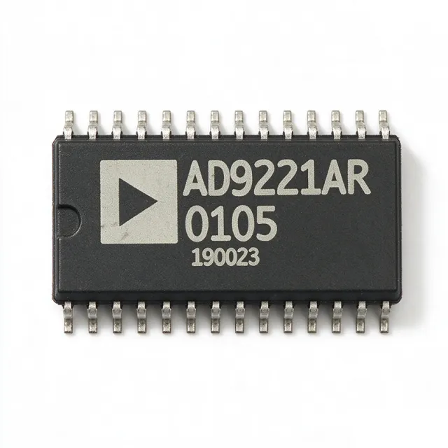
AD9221AR - 12-Bit 1.5 MSPS ADC, 28-SOIC | Analog Devices (Tape & Reel)
AD9221AR

AD9221AR - 12-Bit 1.5 MSPS ADC, 28-SOIC | Analog Devices (Tape & Reel)

The Analog Devices AD9221AR is a monolithic 12-bit, 1.5 MSPS (mega-samples per second) single-supply analog-to-digital converter (ADC) housed in a 28-pin SOIC (Small Outline IC) wide-body package. It features pipelined architecture with true 12-bit linearity, 11.5-bit or better AC performance, and parallel digital output. The wide SOIC package (0.295 inch / 7.50 mm body width) provides robust thermal performance and ease of hand-soldering during prototyping, while tape-and-reel packaging enables high-volume automated assembly. An ADC (analog-to-digital converter) is a semiconductor device that transforms continuous analog voltage signals into discrete digital codes at a defined sampling rate. Within the signal chain hierarchy, the ADC sits between the analog front end (sensor, amplifier, anti-alias filter) and the digital processing block (DSP, FPGA, microcontroller). The 12-bit resolution places the AD9221 in the precision-conversion tier, delivering 4096 discrete output codes (LSB = VREF/4096) suitable for instrumentation, communications, and industrial control where 0.024% quantization steps are acceptable. Key features of the AD9221AR include flexible sampling rates (the AD9221 family spans 1.5, 3.0, and 10.0 MSPS across AD9221/AD9223/AD9220), low power dissipation (a critical advantage for portable and densely-populated designs), on-chip sample-and-hold, and a single +5 V supply operation. The device is pin-compatible with the higher-speed AD9223 (3 MSPS) and AD9220 (10 MSPS), allowing designers to scale sampling rate up or down without PCB rework. The pipelined architecture uses multiple low-resolution stages with inter-stage DACs and digital error correction, producing high throughput at moderate power. A precision bandgap reference and flexible input configuration support both single-ended and differential drive schemes, while the parallel CMOS-compatible digital interface simplifies connection to FPGAs, ASICs, or microcontrollers. Internal calibration ensures specified linearity over temperature. Typical applications include medical imaging (ultrasound front-end digitization), communications IF sampling, instrumentation and test equipment, industrial process control loops, CCD digitizers, and sonar/radar signal processing. Its combination of 12-bit precision with mid-rate sampling suits applications where higher-resolution SAR converters are too slow but full 14-16 bit pipelines are unnecessary. When designing with the AD9221AR, use a low-impedance input buffer (such as the AD8138 or AD8055) to drive the analog inputs, and place the reference bypass capacitor close to the REFCOM and VREF pins. Decouple AVDD and DRVDD separately to prevent digital switching noise from coupling into the analog front end. The wide SOIC footprint allows easy inspection and rework, an advantage for prototype builds. This page synthesizes distributor stock and pricing, drop-in same-family alternatives (AD9220/AD9223), and practical design notes not collected in any single location on the manufacturer datasheet.

USD $16.41 متوفر
AD9221AR-REEL - 12-Bit 1.5 MSPS ADC, 28-SOIC | Analog Devices
AD9221AR-REEL

AD9221AR-REEL - 12-Bit 1.5 MSPS ADC, 28-SOIC | Analog Devices

The Analog Devices AD9221AR-REEL is a monolithic 12-bit, 1.5 MSPS (mega-samples per second) single-supply analog-to-digital converter (ADC) housed in a 28-pin SOIC (Small Outline IC) wide-body package. It features pipelined architecture with true 12-bit linearity, 11.5-bit or better AC performance, and parallel digital output. The wide SOIC package (0.295 inch / 7.50 mm body width) provides robust thermal performance and ease of hand-soldering during prototyping, while tape-and-reel packaging enables high-volume automated assembly. An ADC (analog-to-digital converter) is a semiconductor device that transforms continuous analog voltage signals into discrete digital codes at a defined sampling rate. Within the signal chain hierarchy, the ADC sits between the analog front end (sensor, amplifier, anti-alias filter) and the digital processing block (DSP, FPGA, microcontroller). The 12-bit resolution places the AD9221 in the precision-conversion tier, delivering 4096 discrete output codes (LSB = VREF/4096) suitable for instrumentation, communications, and industrial control where 0.024% quantization steps are acceptable. Key features of the AD9221AR-REEL include flexible sampling rates (the AD9221 family spans 1.5, 3.0, and 10.0 MSPS across AD9221/AD9223/AD9220), low power dissipation (a critical advantage for portable and densely-populated designs), on-chip sample-and-hold, and a single +5 V supply operation. The device is pin-compatible with the higher-speed AD9223 (3 MSPS) and AD9220 (10 MSPS), allowing designers to scale sampling rate up or down without PCB rework. The pipelined architecture uses multiple low-resolution stages with inter-stage DACs and digital error correction, producing high throughput at moderate power. A precision bandgap reference and flexible input configuration support both single-ended and differential drive schemes, while the parallel CMOS-compatible digital interface simplifies connection to FPGAs, ASICs, or microcontrollers. Internal calibration ensures specified linearity over temperature. Typical applications include medical imaging (ultrasound front-end digitization), communications IF sampling, instrumentation and test equipment, industrial process control loops, CCD digitizers, and sonar/radar signal processing. Its combination of 12-bit precision with mid-rate sampling suits applications where higher-resolution SAR converters are too slow but full 14-16 bit pipelines are unnecessary. When designing with the AD9221AR-REEL, use a low-impedance input buffer (such as the AD8138 or AD8055) to drive the analog inputs, and place the reference bypass capacitor close to the REFCOM and VREF pins. Decouple AVDD and DRVDD separately to prevent digital switching noise from coupling into the analog front end. The wide SOIC footprint allows easy inspection and rework, an advantage for prototype builds. This page synthesizes distributor stock and pricing, drop-in same-family alternatives (AD9220/AD9223), and practical design notes not collected in any single location on the manufacturer datasheet.

طلب عرض سعر اتصل بنا
AD9223AR - 12-Bit 3 MSPS ADC | Analog Devices
AD9223AR

AD9223AR - 12-Bit 3 MSPS ADC | Analog Devices

The Analog Devices AD9223AR is a 12-bit, 3.0 MSPS monolithic analog-to-digital converter in a 28-lead SOIC package. It performs parallel-output, single-channel sampling and is positioned between the AD9221 at 1.5 MSPS and the AD9220 at 10.0 MSPS within the AD9221, AD9223, and AD9220 converter family. The family uses a shared interface and pin-compatible 28-lead SOIC and SSOP package options, allowing performance selections to share a common board-level architecture. An ADC is an analog-to-digital converter, a semiconductor that samples continuous analog voltage and represents each sample as a numeric code. In the signal-chain hierarchy, an ADC belongs to data converters and analog-to-digital conversion within broader signal-chain and mixed-signal systems. Parallel output exposes the converted code directly through multiple digital pins, making the device suitable for systems in which a processor, FPGA, or programmable logic device captures the sample bus. The AD9223AR provides 12-bit conversion resolution and a 3.0 MSPS sampling rate. Its 28-pin SOIC package supports conventional surface-mount assembly and compact board layouts. The AD9223 family supports sampling rates of 1.5 MSPS, 3.0 MSPS, and 10.0 MSPS across AD9221, AD9223, and AD9220, respectively. This selection structure supports migration toward higher conversion performance while retaining a common family interface approach. The converter is designed for single-supply operation and uses a pipelined conversion architecture. Pipelined ADC operation divides the conversion into stages that can overlap during successive samples, supporting higher throughput than a single-stage converter operating at the same clock rate. The AD9223AR represents the 3.0 MSPS member of this family, balancing sampling throughput with 12-bit data resolution. Typical uses include industrial data-acquisition systems, communications equipment, instrumentation, embedded signal processing, and test equipment. Its parallel output is particularly appropriate when a downstream digital device can capture data at the converter's sampling rate. System designers should match clocking, analog input bandwidth, reference voltage, output coding, and digital-interface timing to the surrounding signal chain. Board implementation requires careful attention to analog input routing, grounding, decoupling, and digital-output timing. Place input and reference components close to their associated pins, preserve a quiet analog return path, and route the parallel data bus away from sensitive analog nodes. Consult the manufacturer datasheet for the exact pin-description table, recommended application circuit, input-range configuration, and timing values before assigning PCB nets. This page organizes the product identity, sampling-rate position, package information, selection trade-offs, and practical design guidance for engineers comparing the AD9223 with related family members. It also distinguishes exact-orderable alternatives from converters that are only functionally similar, helping avoid substitutions that change pinout, speed, or system timing requirements.

طلب عرض سعر اتصل بنا
AD9225AR - 12-Bit 25 MSPS ADC | Analog Devices
AD9225AR

AD9225AR - 12-Bit 25 MSPS ADC | Analog Devices

The Analog Devices AD9225AR is a monolithic 12-bit, 25 MSPS analog-to-digital converter with an on-chip sample-and-hold amplifier and voltage reference, supplied in a 28-pin SOIC W package. It operates from a single +5 V supply and has a typical power dissipation of 280 mW, making it suitable for compact, high-speed signal-acquisition systems that require parallel digital output. An ADC is a data-conversion IC that samples an analog voltage and converts it into a numeric value. The AD9225 belongs to the pipelined ADC family, a multistage architecture commonly used for conversion rates from tens of megasamples per second to hundreds of megasamples per second. Within the broader semiconductor hierarchy, it is an analog-to-digital converter, data-converter IC, signal-processing IC, and mixed-signal semiconductor. Key features include a 12-bit resolution, a 25 MSPS conversion rate, a guaranteed maximum differential nonlinearity error of 0.4 LSB, and guaranteed no missing codes. The converter includes both its sample-and-hold amplifier and voltage reference on chip, reducing the number of external analog components required. Its parallel output architecture supports direct connection to FPGA, CPLD, or data-capture logic for deterministic sampling throughput. The AD9225 uses a multistage differential pipelined architecture and supports a differential input arrangement with VIN and VINB connections. The manufacturer datasheet recommends centering the analog-input common-mode voltage at approximately 2.5 V by driving VINB from a low-impedance 2.5 V source. With the VREF pin connected directly to SENSE, the reference voltage is 1 V and the corresponding input span is 2 V p-p; the stated valid input-signal range is 1.5 V to 3.5 V. Typical uses include industrial process monitoring, communications infrastructure, digital oscilloscopes, radar and sonar signal chains, waveform capture, and precision control loops. The AD9225 is especially appropriate when 25 MSPS sampling is sufficient and parallel output provides an advantage over serial-interface converters. Its integrated sample-and-hold and reference functions simplify board design while the single +5 V supply reduces multi-rail complexity. The main design trade-off is input bandwidth and signal integrity at 25 MSPS. Differential routing, controlled impedance, a low-noise +5 V supply, proper reference decoupling, and careful return-path management are essential for preserving full-scale accuracy. Engineers should also account for digital-output timing when routing 12 parallel data bits plus clock signals into acquisition logic. This page consolidates the verified manufacturer specifications, current distributor availability, family pin-compatibility information, practical application guidance, and parameter-level replacement analysis. It is designed to help engineers determine whether the AD9225AR fits their acquisition architecture before purchasing or redesigning the board.

طلب عرض سعر اتصل بنا
AD9226ARS - 12-Bit 65 MSPS ADC | Analog Devices
AD9226ARS

AD9226ARS - 12-Bit 65 MSPS ADC | Analog Devices

The Analog Devices AD9226ARS is a 12-bit, 65 MSPS analog-to-digital converter with an on-chip high-performance sample-and-hold amplifier and voltage reference, supplied in a 28-pin SSOP package. It is designed for data-acquisition systems requiring parallel digital output and single-supply operation. The verified product data identifies a monolithic, single-channel, pipelined ADC with differential analog inputs and no missing codes. An ADC is an integrated circuit that converts an analog voltage into a digital numerical value. The AD9226 belongs to the data-converter hierarchy and specifically uses a multistage differential pipeline architecture. Its 65 MSPS sampling rate supports high-speed signal capture, while 12-bit resolution provides 4096 possible digital codes. The internal sample-and-hold amplifier acquires the analog input, and the on-chip voltage reference supports repeatable conversion without requiring a separate reference device. Key features include 12-bit resolution, a 65 MSPS data rate, a single analog input channel, differential input architecture, and parallel output. The converter is specified as a single-supply device. The verified manufacturer listing also describes low-power dissipation and no-missing-code operation. These characteristics make the AD9226ARS suitable for communications, instrumentation, industrial control, test equipment, and other applications where sampled analog waveforms must be digitized rapidly. The AD9226 architecture uses a multistage differential pipeline to implement the conversion. This structure separates the conversion process into successive stages, allowing high throughput compared with a single-stage flash converter. The differential input arrangement can improve rejection of common-mode noise when the source is balanced and the analog front end is correctly implemented. The output interface is parallel, so system designers must account for the timing and routing of the data lines. Typical applications include communications receivers, radar and signal-processing systems, test and measurement instruments, medical instrumentation, industrial process monitoring, and embedded data-acquisition systems. In each case, the input bandwidth, conversion rate, reference accuracy, digital interface, and package availability must be checked against the system requirements before design release. The primary design consideration is ensuring that the analog input bandwidth and external circuitry match the 65 MSPS conversion rate. The sample-and-hold amplifier, voltage reference, power supply, clocking, and digital timing should be evaluated according to the manufacturer datasheet. This page summarizes verified product information and identifies specification fields that require confirmation from the current Analog Devices datasheet.

طلب عرض سعر اتصل بنا
AD9226ARSRL - 12-Bit 65 MSPS ADC | Analog Devices
AD9226ARSRL

AD9226ARSRL - 12-Bit 65 MSPS ADC | Analog Devices

Analog Devices AD9226ARSRL is a 12-bit, 65 MSPS, single-input pipelined analog-to-digital converter with an on-chip sample-and-hold amplifier and voltage reference, supplied in a 28-lead SSOP package. It supports straight binary or two's-complement parallel output data and operates from a single 5 V analog supply with 3 V or 5 V driver supply options. The converter provides 750 MHz full-power bandwidth for wideband signal acquisition. An ADC is a semiconductor that converts continuous analog voltage into a digital representation for processing, storage, or transmission. The AD9226 belongs to the pipelined ADC hierarchy, where multiple internal stages perform successive approximation functions. The resulting 12-bit parallel interface transfers each converted sample directly to digital logic, making the device suitable for data-acquisition systems that require deterministic throughput and broad bandwidth. Key characteristics include 12-bit resolution, a maximum sampling rate of 65 MSPS, and 11.1-bit ENOB at a 10 MHz input frequency. The converter's differential pipeline architecture supports input frequencies beyond the sampling clock because its analog front end has 750 MHz full-power bandwidth. Straight binary and two's-complement output formats provide flexibility when interfacing with FPGAs, DSPs, microprocessors, or data-capture logic. The on-chip sample-and-hold amplifier minimizes the number of external high-frequency analog components, while the internal voltage reference simplifies calibration and board design. A single 5 V analog supply reduces supply complexity compared with dual-supply converter designs. Logic supply voltage can be selected to match 3 V or 5 V digital systems, although the exact clock, timing, and output-valid details should be taken from the manufacturer datasheet before finalizing an interface. Typical uses include communications receivers, industrial data acquisition, RF and IF signal sampling, digital oscilloscopes, control instrumentation, and diagnostic monitoring. The 65 MSPS rate supports a 32.5 MHz Nyquist zone, while 750 MHz full-power bandwidth is valuable when downconversion or direct RF sampling is required. System designers must still account for analog bandwidth, clock jitter, output timing, grounding, decoupling, and FPGA timing closure. For a new design, place the analog input and clock paths on a controlled-impedance board, keep the ADC and its decoupling close together, and provide a low-noise, stable supply. Use the manufacturer's evaluation-board layout and datasheet timing diagrams as the primary implementation references. This page combines verified source data, practical application guidance, and honestly qualified drop-in alternatives for AD9226ARSRL.

طلب عرض سعر اتصل بنا
AD9226ARSZ - 12-Bit 65 MSPS Pipeline ADC | Analog Devices
AD9226ARSZ

AD9226ARSZ - 12-Bit 65 MSPS Pipeline ADC | Analog Devices

The Analog Devices AD9226ARSZ is a monolithic, single-supply, 12-bit, 65 MSPS analog-to-digital converter featuring an on-chip high-performance sample-and-hold amplifier and internal voltage reference, housed in a 28-pin SSOP package. It delivers a differential input range and 65 MSPS conversion rate, consuming only a few hundred milliwatts from a single +5 V supply. An analog-to-digital converter (ADC) is a data converter that transforms continuous analog signals into discrete digital codes for processing by DSPs, FPGAs, and microcontrollers. Pipeline ADCs like the AD9226 use multiple low-resolution flash stages to achieve high sample rates with low latency; they sit within the hierarchy of successive-approximation (SAR), delta-sigma, and flash ADCs, and belong to the broader data-converter family of mixed-signal ICs used in signal-chain and instrumentation systems. Key features include a signal-to-noise ratio of approximately 69 dB, a spurious-free dynamic range (SFDR) of approximately 80 dB, an effective number of bits (ENOB) of 11.1 at fIN = 10 MHz, and a low-power architecture aimed at imaging and communications front-ends. The wideband sample-and-hold input supports differential or single-ended drive with simple passive or active signal conditioning, and the digital outputs provide CMOS-compatible parallel data. Internally the AD9226 uses a multistage differential pipeline architecture with output error-correction logic. The on-chip 2.5 V reference can be left internal or overdriven by an external reference for gain calibration or channel matching in multi-board systems; the data-ready output simplifies interface to FIFOs, DSPs, and FPGAs. Typical applications include medical ultrasound imaging, IF sampling in communications receivers, baseband digital signal processing, instrumentation digitizers, and CCD/camera imaging systems. The combination of 12-bit resolution, 65 MSPS sampling rate, and 28-SSOP footprint makes it a versatile front-end for mid-bandwidth data acquisition. When designing with the AD9226, the most important consideration is using a single +5 V supply rail and providing proper analog input common-mode biasing; bypassing the supply pins with 100 nF and 10 uF ceramic capacitors placed within a few millimetres of each pin maintains rated dynamic performance and minimizes digital coupling into the analog front-end. This page synthesizes distributor pricing, drop-in same-package alternatives, and practical design notes not found in the manufacturer datasheet, helping engineers shorten the selection and PCB procurement cycle.

طلب عرض سعر اتصل بنا
AD9226ARSZRL - 12-Bit 65 MSPS Parallel ADC | Analog Devices
AD9226ARSZRL

AD9226ARSZRL - 12-Bit 65 MSPS Parallel ADC | Analog Devices

The Analog Devices AD9226ARSZRL is a 12-bit, single-channel, 65 MSPS pipelined analog-to-digital converter with a parallel data interface, an integrated voltage reference, and an on-chip sample-and-hold amplifier, packaged in a 28-lead SSOP. An ADC converts an analog voltage into a digital code for processing, instrumentation, communications, or control. The AD9226 belongs to the pipelined ADC family and uses multiple internal stages to achieve high sampling rates while balancing resolution, power, and design complexity. Its 12-bit resolution provides 4096 code levels, while the 65 MSPS sampling rate supports high-speed signal capture. The parallel interface exposes digital conversion results through dedicated output pins and is suitable for systems whose downstream logic can accept the required data timing. Key features include a single-supply architecture, a high-performance sample-and-hold amplifier, an integrated voltage reference, and a multistage differential pipeline. The verified manufacturer information identifies a 65 MSPS data rate, 12-bit resolution, one analog input, and a parallel data interface. The AD9226 also uses CMOS technology and is specified for an industrial temperature range of -40°C to +85°C. Its 28-pin SSOP package is intended for surface-mount assembly, and the AD9226ARSZRL ordering code uses tape-and-reel packaging. The converter is suitable for communications receivers, IF undersampling systems, baseband measurements, industrial signal acquisition, and embedded test equipment. Its pipeline architecture is particularly appropriate when a system needs predictable throughput and digital timing rather than the flexibility of a low-power successive-approximation ADC. The on-chip reference and sample-and-hold amplifier reduce the number of external analog functions required in a basic capture circuit. A key design consideration is the relationship between sampling rate, analog bandwidth, settling behavior, and downstream digital timing. The parallel outputs must be captured correctly by an external FPGA, ASIC, or other digital controller, while the analog input network must provide adequate impedance, bandwidth, and signal integrity. The AD9226ARSZRL is a fixed-function converter, so system flexibility must be provided by the surrounding analog and digital circuitry. Pricing and availability should be checked with authorized distributors as of 2026-10-22 because distributor inventory and lead time can change. This page combines verified manufacturer specifications, distributor listings, package information, and application-oriented design guidance. It also distinguishes confirmed drop-in alternatives from unverified cross-reference candidates so engineers can avoid treating a similar specification as proof of pin compatibility.

طلب عرض سعر اتصل بنا
AD9226AST - 12-Bit 65-MSPS ADC | Analog Devices
AD9226AST

AD9226AST - 12-Bit 65-MSPS ADC | Analog Devices

The Analog Devices AD9226AST is a monolithic 12-bit, 65-MSPS analog-to-digital converter with one differential input pipeline, an on-chip sample-and-hold amplifier, and an on-chip voltage reference in a 48-LQFP surface-mount package. The verified manufacturer information identifies a multistage differential pipeline architecture operating to 65 MSPS and highlights IF undersampling capability for communication receivers. An ADC is an analog-to-digital converter, a data-acquisition IC that samples a continuous analog voltage and represents each sample with a digital code. The AD9226 belongs to the pipeline ADC hierarchy, which uses multistage conversion to support high sampling rates and parallel digital outputs. Its 12-bit resolution provides 4096 possible code levels, while the 65-MSPS rate suits communications, instrumentation, and intermediate-frequency signal chains. The core verified features include a 12-bit resolution, one pipelined differential input, 65 MSPS operation, and integrated sample-and-hold and reference functions. The manufacturer's datasheet also describes undersampling schemes for single-channel communications. Additional performance figures in the provided search material include ENOB of 11.1 bits at a 10 MHz input, intermodulation distortion below -75 dBFS at a 140 MHz input, and guaranteed no-missing-codes operation, though complete test conditions must be taken from the manufacturer datasheet. The AD9226AST uses a single-supply architecture and differential pipeline conversion. Differential signaling helps reduce sensitivity to common-mode noise, while the parallel digital outputs require a correctly timed receiver and controlled PCB routing. Because this is an older high-speed data converter, signal integrity, supply decoupling, clock quality, and output-bus timing are as important as nominal resolution. Typical uses include digital communications receivers, IF undersampling front ends, industrial measurement systems, and instrumentation requiring 12-bit conversion rates up to 65 MSPS. A suitable design should provide a low-jitter sampling clock, matched input-network values, solid reference and supply bypassing, and controlled impedance for high-speed digital traces. The principal design trade-off is throughput versus resolution: 65 MSPS is useful for wideband or undersampled signals, but 12-bit conversion does not provide the precision of higher-resolution ADCs. Confirm input bandwidth, analog range, output timing, and package-level land-pattern requirements against the manufacturer datasheet before production release. This page combines verified manufacturer and distributor information with application guidance, compatibility cautions, and source-linked technical context. Pricing, stock, lifecycle status, and full pin-level data are not stated in the supplied records and therefore are not inferred here.

طلب عرض سعر اتصل بنا
AD9226ASTRL - 12-Bit 65 MSPS ADC | Analog Devices
AD9226ASTRL

AD9226ASTRL - 12-Bit 65 MSPS ADC | Analog Devices

The Analog Devices AD9226ASTRL is a 12-bit, 65 MSPS, single-input pipelined analog-to-digital converter with an on-chip sample-and-hold amplifier and voltage reference, supplied in a 48-LQFP 7 x 7 mm package. It accepts a 5 V nominal supply, supports a -40°C to +85°C operating-temperature range, and uses a parallel data interface. The converter is designed for high-speed signal capture, IF undersampling, communications equipment, and instrumentation requiring more than 12-bit resolution at a 65 MSPS sampling rate. An ADC is a data-conversion IC that transforms an analog voltage into a numeric code for processing by an FPGA, DSP, microcontroller, or other digital logic. The AD9226 belongs to the pipeline ADC family within the broader ADC and data-converter hierarchy. Its multistage differential pipeline architecture samples continuously at 65 MSPS, while the integrated sample-and-hold amplifier reduces the external component count required at the analog input. The parallel interface exposes the converted data directly to digital circuitry rather than relying on a high-speed serial link. Key device characteristics include 12-bit resolution, a 65 MSPS data rate, one analog input, and a differential pipeline architecture. The integrated high-performance sample-and-hold amplifier is specifically suited to IF undersampling schemes, including single-channel communication applications operating at input frequencies up to and beyond the Nyquist rate. Published distributor information also reports 11.1 bits ENOB at a 10 MHz input frequency and approximately -75 dBFS intermodulation distortion at a 140 MHz input frequency. The converter's monolithic implementation combines the sampling front end, pipeline stages, digital correction logic, and voltage-reference options in one package. The manufacturer datasheet describes internal reference-voltage configurations that can generate reference levels between 1 V and 2 V, as well as an external-reference option for designs requiring enhanced accuracy or drift performance. Because it uses a differential pipeline architecture, board-level implementation must preserve controlled impedance, symmetrical routing, and clean separation between analog and digital return paths. Typical uses include digital oscilloscopes, communications receivers, IF-sampling front ends, radar and signal-processing systems, industrial measurement equipment, and laboratory instrumentation. At 65 MSPS, the device can capture substantially faster waveforms than low-speed general-purpose ADCs while retaining 12-bit resolution. It is also appropriate where undersampling allows a band-limited RF signal to be converted directly without first downconverting it to baseband. The primary design consideration is analog-input implementation. The AD9226 offers internal and external reference options, but the selected mode affects accuracy, drift, and circuit complexity. Designers should also account for input bandwidth, output timing, parallel-bus skew, supply decoupling, and the difference between analog and digital signal integrity when laying out a 48-LQFP PCB. This page combines verified manufacturer and distributor information with application guidance, interface considerations, and a conservative replacement analysis. It distinguishes documented AD9226 family options from unsupported cross-package substitutes and explicitly identifies data that requires confirmation from the datasheet or current distributor inventory.

طلب عرض سعر اتصل بنا
AD9226ASTZ - 12-Bit 65 MSPS ADC | Analog Devices
AD9226ASTZ

AD9226ASTZ - 12-Bit 65 MSPS ADC | Analog Devices

The Analog Devices AD9226ASTZ is a 12-bit, 65 MSPS, single-channel pipelined analog-to-digital converter with an on-chip sample-and-hold amplifier and voltage reference, supplied in a 48-LQFP 7 mm x 7 mm package. It provides a parallel 12-bit data interface and operates from a single 5 V supply. The converter is designed for high-speed signal acquisition, IF undersampling, communications, instrumentation, and industrial imaging systems. An ADC is an analog-to-digital converter, a semiconductor that samples an analog voltage and produces a corresponding digital code. The AD9226 belongs to the pipelined ADC family, using multiple internal stages to convert each sample at a high throughput. Its 65 MSPS rating means the converter can acquire up to 65 million samples per second, while the 12-bit resolution represents each sample with 4096 digital codes. The parallel interface simplifies connection to FPGAs, CPLDs, DSPs, and digital capture systems. The AD9226ASTZ provides a single analog input, a differential pipeline architecture, an integrated voltage reference, and a single-supply operating design. According to the Analog Devices product page and datasheet, the device is intended for communications receivers and IF undersampling schemes, including input frequencies above the traditional Nyquist region when supported by the system design. The 12-bit resolution is suitable for many communication and measurement systems where compact digital resolution and high sample throughput are more important than very high conversion resolution. The device uses a parallel data output rather than a serial LVDS interface. This can simplify timing at moderate board speeds, but it requires routing 12 data lines plus clock and control signals on the PCB. The LQFP package provides a familiar surface-mount footprint, while the exposed package area and thermal design must be handled according to the manufacturer datasheet and board-level thermal requirements. Input and reference routing are performance-sensitive because clock, analog, digital, and return currents should be separated carefully. Typical uses include digital RF receivers, IF signal capture, communications test equipment, oscilloscope and waveform-analysis systems, industrial measurement, and embedded signal-processing platforms. A clock source must meet the converter's timing and jitter requirements, and the analog input network must provide the appropriate impedance and bandwidth. Firmware and hardware should account for the parallel output latency, clock polarity, data-valid timing, settling time, and calibration or offset behavior of the complete acquisition chain. When selecting this converter, compare resolution, sampling rate, input bandwidth, output interface, supply voltage, package, operating temperature, and system clocking rather than relying on resolution alone. This page summarizes verified manufacturer and distributor information while clearly separating specifications that were not supplied from design-dependent values that require board-level validation.

طلب عرض سعر اتصل بنا
AD9226ASTZRL - 12-Bit 65 MSPS ADC | Analog Devices
AD9226ASTZRL

AD9226ASTZRL - 12-Bit 65 MSPS ADC | Analog Devices

The Analog Devices AD9226ASTZRL is a 12-bit, single-channel, 65 MSPS pipelined analog-to-digital converter with an integrated sample-and-hold amplifier and voltage reference, supplied in a 48-LQFP 7 mm × 7 mm package. It is designed for high-speed signal conversion where a parallel output interface and single-supply operation simplify connection to digital control, communications, instrumentation, and test systems. The verified product information identifies a 1-input architecture, industrial temperature range of -40°C to +85°C, and tape-and-reel packaging. An ADC converts an analog voltage into a digital numeric representation. The AD9226 belongs to the pipeline ADC category, where multistage internal converters operate with a latency between sampling and output availability. Its 12-bit resolution provides 4,096 digital codes, while the 65 MSPS sampling rate supports acquisition of rapidly changing signals. The integrated sample-and-hold amplifier captures the input during the sampling interval, and the internal voltage reference helps reduce the need for external reference circuitry. Key verified features include 12-bit resolution, 65 MSPS throughput, one analog input, a differential pipeline architecture, a parallel data interface, and a 48-LQFP package. The manufacturer describes the device as a monolithic, single-supply ADC fabricated on an advanced CMOS process. The sample-and-hold amplifier is specifically suited to IF undersampling schemes, including single-channel communication applications where input frequencies can reach or exceed the Nyquist frequency. The AD9226 is appropriate for communications receivers, RF and IF signal-chain conversion, radar-related instrumentation, industrial measurement systems, and digital signal-processing front ends. Because the converter uses a parallel output, the surrounding system must provide compatible digital voltage levels, sufficient data capture timing, clocking, grounding, and decoupling. The 48-LQFP footprint is suitable for conventional surface-mount assembly but requires careful attention to analog signal integrity and clock jitter. A key design consideration is ensuring that the analog input, reference, and clock paths have appropriate impedance and return paths. The datasheet should be consulted for the exact pinout, input range, output coding, timing, supply requirements, and recommended application circuit because those details are not fully available in the supplied distributor excerpts. The verified data identifies the industrial package and temperature grade, but it does not provide enough information to fabricate all electrical parameters. This page combines verified manufacturer and distributor information with package, application, selection, and design guidance. It is intended to help engineers identify the AD9226ASTZRL for high-speed conversion while clearly separating confirmed specifications from parameters that require confirmation in the official datasheet.

طلب عرض سعر اتصل بنا
AD9228ABCPZRL7-40 - Quad 12-Bit 40 MSPS Serial LVDS ADC | ADI
AD9228ABCPZRL7-40

AD9228ABCPZRL7-40 - Quad 12-Bit 40 MSPS Serial LVDS ADC | ADI

The Analog Devices AD9228ABCPZRL7-40 is a quad, 12-bit, 40 MSPS analog-to-digital converter (ADC) with an on-chip sample-and-hold circuit, packaged in a 48-lead LFCSP-VQ (7x7 mm) with exposed pad and shipped on a 7-inch reel. It integrates four pipelined ADC channels into a single package, delivering 119 mW per channel at 65 MSPS and supporting a 1.8 V analog/digital supply. The SNR is 70 dB to Nyquist with an ENOB of 11.3 bits and SFDR of 82 dBc, making it suitable for cost- and power-sensitive multi-channel systems. An analog-to-digital converter is a mixed-signal integrated circuit that samples continuous-time analog signals and converts them to discrete digital codes for downstream DSP, FPGA, or processor consumption. Within the signal-chain taxonomy, the AD9228 sits as an ADC -> data converter -> mixed-signal IC -> semiconductor. Pipelined ADCs like this one achieve high sampling rates by cascading low-resolution stages, trading latency for throughput. Key features include 4 ADCs integrated into 1 package, a serial LVDS digital interface that reduces board-routing complexity and EMI, SPI-compatible configuration registers for per-channel gain and offset trim, and an operating temperature range of -40C to +85C. The LFCSP-VQ-48 footprint provides a low thermal resistance path through the exposed pad, enabling the quad converter to operate at full speed without external heatsinking in typical ambient conditions. The AD9228ABCPZRL7-40 is optimized for low cost, low power, and small size, while its pin-compatible 65 MSPS speed grade (AD9228ABCPZRL7-65) lets designers select the sample rate on the same PCB footprint. The integrated sample-and-hold circuit on each channel ensures matched timing skew across the four inputs, simplifying calibration in phased-array and quadrature receivers. Typical applications include medical imaging, communications base-station receivers, portable and handheld instrumentation, multichannel data acquisition, and ultrasound. Engineers choose the AD9228ABCPZRL7-40 when they need four synchronized 12-bit channels at 40 MSPS with LVDS output in a compact 7x7 mm CSP footprint. When designing with this device, ensure the exposed pad is soldered to a sufficiently large copper pour to maintain junction temperature within the -40C to +85C operating range. Decouple AVDD and DRVDD separately and place 0.1 uF bypass capacitors as close to each supply pin as possible. This page synthesizes distributor pricing, drop-in alternatives, and practical design notes not found in the manufacturer datasheet, helping engineers evaluate the AD9228ABCPZRL7-40 alongside ADI's broader quad-ADC portfolio.

طلب عرض سعر اتصل بنا
AD9228BCPZ-40 - Quad 12-bit 40 MSPS Serial LVDS ADC | Analog Devices
AD9228BCPZ-40

AD9228BCPZ-40 - Quad 12-bit 40 MSPS Serial LVDS ADC | Analog Devices

The Analog Devices AD9228BCPZ-40 is a quad, 12-bit, 40 MSPS analog-to-digital converter (ADC) with four on-chip sample-and-hold circuits, housed in a 48-pin LFCSP-VQ (7x7 mm) package. It integrates four ADCs into a single device, consumes 119 mW per channel at 65 MSPS, and serializes the conversion data over ANSI-644 LVDS links for low-pin-count board routing. An ADC (analog-to-digital converter) is a semiconductor device that converts continuous-time analog signals into discrete digital codes at a defined sample rate. The AD9228 belongs to the pipelined ADC family within the broader data-converter category, sitting between sigma-delta (high-resolution, low-speed) and SAR (medium-resolution, high-speed) converters. Quad ADCs are used when multiple channels must be sampled simultaneously - typically in medical imaging, communications base stations, and multi-antenna receivers - because integrated quad parts reduce board area, BOM cost, and channel-to-channel timing skew versus four discrete ADCs. Key specifications include 70 dB SNR to Nyquist, 11.3-bit effective number of bits (ENOB), 82 dBc spurious-free dynamic range (SFDR) to Nyquist, ±0.3 LSB typical DNL and ±0.4 LSB typical INL. The -40 speed grade limits operation to 40 MSPS maximum; the higher-grade AD9228BCPZ-65 variant shares the same package and runs up to 65 MSPS. Programmable clock and data alignment plus built-in digital test pattern generation (deterministic, pseudo-random, and user-defined via SPI) simplify board bring-up and ATE test. Typical applications include medical ultrasound beamforming receivers, multi-channel communications IF digitization, portable instrumentation, and multi-antenna software-defined radio front ends. The 1.8 V analog supply and LVDS digital interface minimize EMI and ease interface to modern FPGAs such as the Xilinx 7-series and Intel Cyclone families. When designing with the AD9228, route analog inputs as 50 ohm differential pairs and place decoupling capacitors within 5 mm of each supply pin. Match trace lengths across the four channels when simultaneous sampling is required - the device's internal timing skew specification confirms the maximum acceptable mismatch budget. This page synthesizes distributor pricing, drop-in alternative analysis, and practical design notes that are not aggregated on the manufacturer datasheet alone.

طلب عرض سعر اتصل بنا
AD9235BRURL7-40 - 12-Bit 40 MSPS 3V ADC | Analog Devices
AD9235BRURL7-40

AD9235BRURL7-40 - 12-Bit 40 MSPS 3V ADC | Analog Devices

The Analog Devices AD9235BRURL7-40 is a 12-bit, 40 MSPS, single 3 V supply, monolithic pipelined analog-to-digital converter housed in a 28-pin TSSOP (RU) surface-mount package. The device integrates a high-performance sample-and-hold amplifier (SHA), an internal voltage reference, and an on-chip duty-cycle stabilizer to maximize dynamic performance across varying input clock duty cycles. It is the 40 MSPS speed-grade variant within the broader AD9235 family, which also includes 20 MSPS and 65 MSPS versions. A pipelined ADC is a multi-stage converter architecture that processes samples in parallel sub-stages, achieving high sampling rates while keeping per-stage power dissipation low. Pipelined ADCs, in the broader ADC hierarchy, sit between successive-approximation-register (SAR) converters and flash converters, combining moderate resolution (typically 8-16 bits) with high throughput (tens to hundreds of MSPS). They are widely used in communications, instrumentation, and imaging applications where speed and resolution must be balanced against power and cost. Key features of the AD9235BRURL7-40 include a fully differential SHA input that supports user-selectable input ranges and offsets (single-ended or differential), an internal 2.5 V bandgap reference (external reference option available), CMOS-compatible digital outputs, and low power dissipation of approximately 110 mW at 40 MSPS with 3 V supply. The wide input bandwidth SHA handles multiplexed systems that switch full-scale voltage levels in successive channels and supports undersampling of IF signals well beyond the Nyquist rate. Operating temperature range spans -40°C to +85°C, making it suitable for industrial environments. Typical applications include communications IF sampling, portable and battery-powered imaging systems, multichannel multiplexed data acquisition, handheld oscilloscope front-ends, and cable-modem downstream receivers. The on-chip reference and small TSSOP footprint reduce external BOM, enabling compact designs. When using the internal reference, decouple REFT and REFB pins with high-quality ceramic capacitors; for best SFDR in multitone IF applications, the external reference mode is recommended.

طلب عرض سعر اتصل بنا
AD9235BRURL7-65 - 12-Bit 65 MSPS ADC, 3V, TSSOP-28 | Analog Devices
AD9235BRURL7-65

AD9235BRURL7-65 - 12-Bit 65 MSPS ADC, 3V, TSSOP-28 | Analog Devices

The Analog Devices AD9235BRURL7-65 is a 12-bit, 65 MSPS pipelined analog-to-digital converter (ADC) operating from a single 3 V supply, housed in a 28-pin TSSOP package. It is a member of the AD9235 family that offers 20/40/65 MSPS speed grades, with this specific order code shipping in tape-and-reel packaging (the "RL7" suffix designates the 7-inch reel). The 65 MSPS variant provides a 70 dBFS SNR to Nyquist and 85 dBFS SFDR to Nyquist, supporting high-fidelity intermediate-frequency sampling in communication receivers. An ADC (analog-to-digital converter) is a semiconductor device that converts a continuous analog voltage into a discrete digital code at a sampling rate set by an external clock. Pipelined ADCs like the AD9235 use a multi-stage architecture that enables high sample rates at low power, while 12-bit resolution is the workhorse for cellular base stations, ultrasound imaging, and instrumentation. Within the broader taxonomy, the AD9235 sits in the data-converter category of mixed-signal ICs. Key features of the AD9235BRURL7-65 include a differential analog input with 500 MHz bandwidth, an on-chip sample-and-hold amplifier (SHA), an internal voltage reference, and ±0.4 LSB differential non-linearity (DNL). The analog input range scales from 1 V p-p to 2 V p-p, output data is available in offset-binary or twos-complement format, and an integrated clock-duty-cycle stabilizer (DCS) relaxes clock-source requirements. A proprietary front-end SHA driving the pipelined core allows IF-sampling well beyond the Nyquist limit, useful in undersampling radio receivers. Power consumption is 300 mW at 65 MSPS, and a flexible LVCMOS/TTL-compatible parallel digital interface simplifies FPGA/CPLD downstream connections. Typical applications include communications IF sampling, ultrasound and medical imaging front-ends, low-cost instrumentation, and high-speed data acquisition cards. Designers value the part when a low-power, single-supply 12-bit ADC in a compact surface-mount footprint is needed. When laying out the PCB, keep analog and digital grounds separated and join them at a single point near the ADC to limit return-path noise; place the input anti-alias filter as close as practical to the analog inputs and use a stable, low-jitter clock source to preserve SNR and SFDR. This page synthesizes distributor pricing, pin-compatible drop-in alternatives, and PCB-level design notes not found in the manufacturer datasheet, helping engineers select the right speed grade and validate second-source supply.

طلب عرض سعر اتصل بنا
AD9237BCPZ-20 - 12-Bit 20 MSPS ADC 3V Low Power LFCSP-32
AD9237BCPZ-20

AD9237BCPZ-20 - 12-Bit 20 MSPS ADC 3V Low Power LFCSP-32

The Analog Devices AD9237BCPZ-20 is a 12-bit, 20 MSPS monolithic analog-to-digital converter (ADC) that operates from a single 3 V supply in a 32-lead LFCSP-WQ (5x5 mm) package. It features an integrated high-performance sample-and-hold amplifier (SHA), an on-chip voltage reference, and selectable input ranges from 1 V p-p to 4 V p-p for flexible signal conditioning. An ADC (analog-to-digital converter) is a data-acquisition integrated circuit that samples continuous analog waveforms and converts them into discrete digital codes for downstream DSP, microcontrollers, or FPGAs. ADCs form a critical link in the signal chain between analog transducers (sensors, antennas, IF stages) and digital processors, and high-speed variants such as the AD9237 typically employ pipelined architectures for high sampling rates at moderate resolution. Within the broader taxonomy, the AD9237BCPZ-20 belongs to the family of pipeline ADCs, which sit between successive-approximation (SAR) ADCs (low-power, multi-MHz) and high-speed flash/serial-lvds ADCs (hundreds of MSPS). Key differentiating specifications include ultralow power dissipation at 20 MSPS, differential analog inputs with 500 MHz full-power bandwidth, and excellent dynamic performance that includes SNR of up to 66 dBc to Nyquist and SFDR of 80 dBc to Nyquist at 65 MSPS. The part also offers DNL of ±0.7 LSB, an output enable pin for multiplexing, and CMOS-compatible digital outputs. These specifications make it well suited for imaging, communications IF sampling, and portable instrumentation. Architecturally, the AD9237 uses a multistage differential pipelined topology with output error correction logic. The on-chip reference and SHA minimize external component count, while the selectable input-span feature allows direct coupling to a wide range of op-amp and transformer front ends without external attenuators. Typical applications include ultrasound and medical imaging front ends, communications IF sampling in software-defined radios, handheld test instruments, and low-power industrial data acquisition modules. Designers often select the AD9237BCPZ-20 when migrating from the pin-compatible AD9235 for additional speed headroom. A key design consideration is proper layout of the analog and digital grounds and the use of low-noise LDOs on the 3 V supply rail to preserve SNR. The output enable pin should be tied properly to avoid bus contention during multi-ADC multiplexing. This page synthesizes distributor pricing, drop-in alternatives, and practical design notes beyond what the manufacturer's datasheet alone provides.

طلب عرض سعر اتصل بنا