دوائر التوصيل البيني المتكاملة
الفئات الفرعية
المنتجات (2,200+)

VSP3200Y-2K - 16-Bit 8MSPS CCD Signal Processor | Texas Instruments
The Texas Instruments VSP3200Y-2K is a 16-bit, 8 MSPS, 3-channel analog front end (AFE) signal processor for CCD, CMOS, and CIS image sensors, housed in a 48-pin LQFP (7x7 mm) package and operating from a single +5V supply. An analog front end for image sensors is the circuit block between the imaging array and the digital image processor. It performs correlated double sampling (CDS) to remove reset noise and kTC noise from the CCD output, applies programmable gain to normalize signal amplitude across color channels, and digitizes the conditioned signal with a high-resolution ADC. Within the system hierarchy, the AFE sits inside the imaging signal chain: image sensor -> AFE (CDS + PGA + ADC) -> DSP/ASIC -> host interface. Key features of the VSP3200Y include three Correlated Double Samplers (CDSs) and three Programmable Gain Amplifiers (PGAs) that process CCD signals from 3-channel (RGB) scanners, a 16-bit conversion path running at up to 8 MSPS, dual output mode for flexible host interfacing, and single +5V operation that simplifies power tree design in desktop scanner platforms. Technically, the VSP3200Y integrates the complete analog processing chain for CCD signal conditioning: the CDS stages sample the pixel signal twice to cancel low-frequency drift and reset noise, the PGAs allow per-channel gain calibration, and the internal 16-bit ADC delivers 8 Msps throughput. Interface compatibility with the VSP3210 single-chip product, which is itself pin-to-pin compatible with the VSP3100 in demultiplexed output mode, provides a migration path for higher integration designs. Typical applications are flatbed and document scanners using CCD or CIS linear arrays, industrial inspection cameras, and desktop imaging peripherals that require 16-bit depth at moderate 8 MSPS speeds. A key design consideration is layout of the analog ground and the CCD output trace: keep the sensor-to-CDS input path short, guard it from digital output drivers, and provide a clean +5V rail with local decoupling, because residual reset noise not removed by the CDS directly limits the effective 16-bit resolution. This page synthesizes distributor inventory, drop-in alternatives, pricing tiers, and practical design notes not found in the manufacturer datasheet.

W5100 - 10/100 Ethernet Controller with TCP/IP | WIZnet
WIZnet W5100 is a single-chip Internet-enabled 10/100 Ethernet controller for embedded systems, integrating TCP/IP, MAC, and PHY functions in an 80-LQFP 10 x 10 mm package. The controller supports 10/100 Base-T/TX Ethernet connectivity through an SPI interface, reducing the need for a host processor to manage low-level network stacks. An Ethernet controller is an interface IC that connects an embedded processor to a physical network. In the W5100, the MAC, TCP/IP hardware, and 10/100 PHY are integrated into one device, allowing the host MCU or CPU to communicate through SPI while the controller handles Ethernet framing and protocol processing. The verified distributor listing identifies W5100 as a 10/100 Base-T/TX Ethernet controller with an SPI interface and an 80-LQFP package. The manufacturer datasheet describes the device as a full-featured, single-chip Internet-enabled controller designed for embedded applications where integration stability, performance, area, and system cost control are important. W5100 is suited to industrial embedded equipment, control systems, instrumentation, building automation, and other Ethernet-connected products. Its integrated architecture can simplify hardware design by combining the Ethernet MAC and PHY with hardware-assisted TCP/IP functions, while the SPI host interface keeps the external processor interface compact. The 10/100 Ethernet capability makes W5100 appropriate for legacy and cost-sensitive networks operating at 10 or 100 Mbit/s. The exact PHY, electrical, timing, temperature, memory, and SPI operating details should be confirmed directly in the manufacturer datasheet before final schematic, layout, and qualification decisions. The W5100 is not a power semiconductor, so a safe operating area is not applicable. Proper implementation requires attention to Ethernet magnetics, RJ45 integration, PCB signal integrity, power sequencing, decoupling, and the exact pin assignments shown in the official documentation. This page consolidates the verified product description, distributor package information, datasheet links, and engineering-oriented application guidance.

W5500 - Hardwired TCP/IP Ethernet Controller SPI | WIZnet
The WIZnet W5500 is a hardwired TCP/IP embedded Ethernet controller that integrates the TCP/IP stack, 10/100 Ethernet MAC, and PHY in a single chip, communicating to a host MCU over an SPI bus at up to 80 MHz. It provides 8 simultaneous sockets with 32 KB of internal TX/RX buffer memory and is housed in a 48-pin LQFP (7x7 mm) package. An Ethernet controller (also called a network controller or NIC controller) is a semiconductor device that offloads the low-level networking functions - framing, MAC addressing, PHY transceiver signaling, and protocol handling - from the host microcontroller. Hardwired TCP/IP controllers go further by implementing the TCP, UDP, IPv4, ICMP, PPPoE, ARP, and IGMP protocols in dedicated silicon rather than firmware. Within the broader taxonomy, the W5500 sits at: Ethernet controller -> network controller -> communication IC -> semiconductor. Compared to a microcontroller running an LWIP software stack, a hardwired controller delivers deterministic latency, low MCU overhead, and a smaller code footprint, but lacks the flexibility of full-protocol software stacks. Key features include 10/100 Base-TX auto-negotiation, full/half-duplex operation, 8 independent socket buffers, a wake-on-LAN (WoL) pin for remote wake scenarios, and integrated 802.3az energy-efficient Ethernet support. The SPI interface runs from 0 to 80 MHz in variable-length mode and supports Mode 0 / Mode 3, allowing direct connection to most ARM Cortex-M, ESP32, AVR, and PIC hosts without glue logic. The W5500's architecture is built around a hardwired protocol engine and dedicated socket memory blocks. Each of the 8 sockets has a Tx buffer and Rx buffer routed through an internal DMA-like engine, so the host MCU does not have to manage TCP state machines. The embedded PHY supports HP Auto-MDIX, eliminating the need for crossover cables. Compared to the legacy W5100 (80-pin), the W5500 reduces pin count to 48 and adds SPI efficiency improvements, while W5100S retains the 80-pin footprint for drop-in W5100 upgrades. Typical applications include IoT sensor nodes, industrial Ethernet PLCs, smart-home gateways, IP-camera control planes, and Arduino/MCU Ethernet shields. The 32 KB buffer is sufficient for most MQTT/CoAP/HTTP payloads without external memory, and the SPI bus allows the part to be wired directly to microcontrollers that lack integrated Ethernet MAC/PHY. Design consideration: because the W5500 integrates the PHY, the board must route the MDI differential signals as a 100-ohm differential pair and provide a 1:1 center-tap magnetics module. Decouple both 3.3 V analog and digital rails at the chip pins with 0.1 uF and 10 uF ceramics; share ground with the host MCU through a single stitch. This page synthesizes distributor pricing, same-family drop-in alternatives, and practical hardware-design notes not consolidated in the manufacturer datasheet.
W6300-L - IPv4/IPv6 Hardwired TCP/IP Ethernet Chip | WIZnet
The WIZnet W6300-L is a hardwired TCP/IP Ethernet controller chip that integrates a dual IPv4/IPv6 protocol stack in hardware, delivering 10/100 Mbps Ethernet performance for embedded systems in an LQFP-48-EP (7x7 mm) surface-mount package. A hardwired TCP/IP controller is a type of offload engine (TOE - TCP/IP Offload Engine) in the broader hierarchy of network interface ICs. Unlike software stacks running on a host MCU, a hardware protocol stack offloads TCP, UDP, ICMP, ARP, and related processing from the main processor, so even a small 8-bit MCU can implement reliable network connectivity with minimal firmware overhead and deterministic timing. This makes the category essential for industrial automation, IoT gateways, and embedded networking nodes. Key features of the W6300-L include the dual IPv4/v6 hardware stack, which sets it apart from WIZnet's earlier IPv4-only devices; multiple independent hardware sockets for simultaneous connections; a high-speed host interface for fast data throughput; and low-power operation modes for energy-sensitive designs. According to the WIZnet product page, the chip combines high-speed Ethernet performance with advanced power efficiency. Technically, the W6300 continues WIZnet's well-established W-series architecture: socket registers, internal TX/RX buffers, PHY, and MAC are all integrated, so designers need only an external RJ45 magnetics jack and a host MCU to complete the network node. The hardware stack eliminates porting, memory-footprint, and real-time concerns associated with software TCP/IP stacks such as lwIP. Typical applications include industrial automation and factory networking, IoT gateways bridging field devices to cloud backends, and embedded equipment requiring IPv6 readiness for modern network infrastructure. For design consideration, verify host-interface timing against your MCU's SPI or bus clock, and follow the WIZnet reference schematic for magnetics, crystal, and decoupling placement to guarantee PHY signal integrity. This page synthesizes distributor pricing, drop-in alternatives, design notes, and AEO-optimized FAQs not found in the manufacturer datasheet.

WGI210AT - Intel I210-AT Gigabit Ethernet Controller QFN-64 | Intel
The Intel WGI210AT (also marketed as the Intel Ethernet Controller I210-AT) is a single-chip, PCIe-based Gigabit Ethernet controller that supports 10BASE-T, 100BASE-TX, and 1000BASE-T operation, packaged in a 9 mm x 9 mm 64-pin QFN with an exposed thermal pad. It integrates a PCIe v2.1 (2.5 GT/s) host interface, a GMII/RGMII/MII MAC, and on-chip PHY, delivering full IEEE 802.3 compliance for enterprise, industrial, and embedded networking designs. The device uses a 0.9 V internal core supply with a 3.3 V I/O supply, enabling low power consumption typical of 1 W class GbE controllers. A Gigabit Ethernet controller is a purpose-built networking IC that links a host processor (typically via PCIe) to a copper or fiber physical network, handling MAC/PHY framing, link training, and TCP/UDP/IP checksum offload. Within Intel's Ethernet controller taxonomy, the I210 sits in the lower-power mainstream tier below the I350/I210 server parts, optimized for single-port embedded and small-form-factor designs. PCIe is the standard host interconnect for these controllers, replacing the older PCI-X interfaces that preceded the GbE era. Key features include TimeSync offload (IEEE 1588/802.1AS) for industrial automation, energy-efficient Ethernet (EEE) per IEEE 802.3az, jumbo frame support up to 9.5 KB, and the proven Intel PROSet driver stack. The exposed pad of the QFN-64 package provides a low-thermal-resistance path to the host PCB, a critical feature since GbE PHYs can dissipate 600 mW to 1.2 W during continuous full-duplex operation. On-die MACsec and VLAN stripping/insertion further reduce host CPU overhead. Architecturally, the I210 uses a PCI Express 2.1 endpoint controller with one x1 lane, hardware IEEE 802.1Qav time-sensitive-networking shaping, and an integrated 1000BASE-T PHY capable of auto-negotiation across all three link rates. The MAC supports 9.6 KB jumbo frames, IPv4/IPv6 checksum offload, TCP segmentation offload (TSO v2), and iSCSI boot for SAN-attached storage platforms. This combination of MAC, PHY, and PCIe in a single 64-pin QFN distinguishes the I210 from external-PHY controllers. Typical applications include industrial PCs, factory automation controllers, point-of-sale terminals, network printers, embedded routers, and small business servers. For automotive and industrial-grade designs with extended temperature requirements, Intel offers the pin-compatible WGI210IT variant rated for -40 C to +85 C operation rather than the 0 C to +70 C commercial range of the WGI210AT. When designing with this controller, allocate at least four PCB layers with a continuous ground plane beneath the QFN-64 exposed pad to keep junction temperature below 110 C; provide 4 kV ESD protection on the MDI lines; and verify driver compatibility with your OS kernel (Windows, Linux, VxWorks, or RTOS). The PCIe reference clock must be a 100 MHz HCSL source with the impedance and jitter specified in the Intel I210 datasheet. This page synthesizes distributor pricing as of 2026-10-11, drop-in alternatives from the same I210 family, and practical layout notes that complement the Intel datasheet with cross-reference insight not found on a single OEM page.
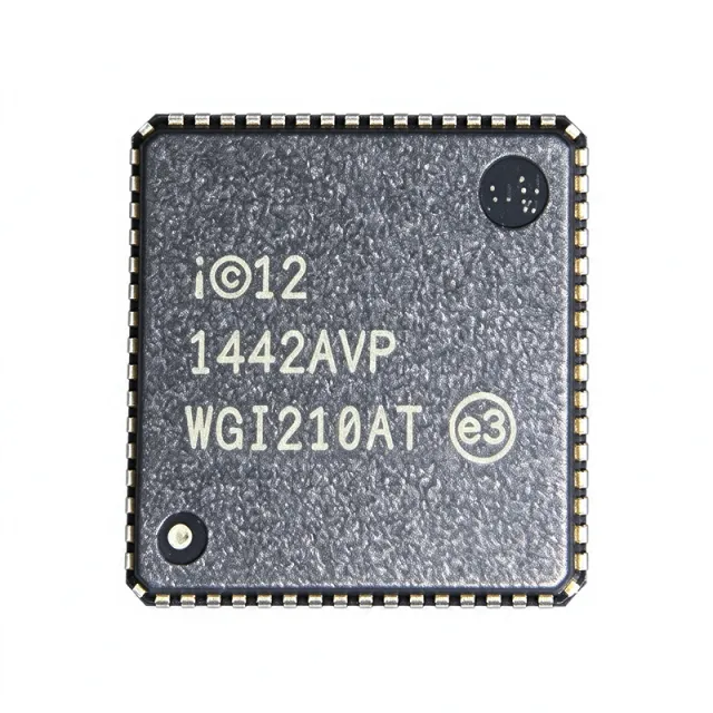
WGI210AT-SLJXR - Intel I210-AT GbE Ethernet Controller QFN-64
The Intel WGI210AT-SLJXR is an Intel Ethernet Controller I210-AT single-chip Gigabit Ethernet MAC + PHY in a 9x9 mm QFN-64 (9x9) package, supporting 10BASE-T, 100BASE-TX, and 1000BASE-T over PCIe, SGMII, SPI, JTAG, and I2C interfaces at 3.3 V supply and 0.9 V core. According to the I210-AT datasheet, the device integrates a GbE PHY with jumbo-frame support and Audio-Video Bridging / IEEE 802.1AS / 802.3az Energy Efficient Ethernet features for desktop, server, and embedded designs. An Ethernet controller is a mixed-signal integrated circuit that links a host system (typically a CPU or SoC) to a wired network, handling MAC address framing, PHY physical-layer termination, and offloading protocol tasks from the host CPU. It belongs to the broader network-interface category (NIC controller -> Ethernet controller -> mixed-signal IC -> semiconductor) and is essential wherever a deterministic, low-latency wired network connection is required. Ethernet controllers sit in the platform's input/output subsystem, bridging PCIe to copper media and providing the physical termination that magnetics and an RJ45 jack connect to. The I210-AT is Intel's mainstream GbE controller for non-server applications and supports the full media-negotiation trio of 10 Mbps, 100 Mbps, and 1000 Mbps. It exposes a PCIe v2.1 5 GT/s host interface for typical x1 edge-connector applications, alongside legacy SMBus, SPI, and JTAG for management and firmware update. Power is supplied through a 3.3 V main rail and a 0.9 V core rail, with full PHY-level Energy Efficient Ethernet (EEE) support reducing link power during idle periods. Industrial features include NC-SI / SMBus manageability, MAC address pre-programming, and platform firmware resiliency. Typical applications of the I210-AT include desktop and workstation motherboards (as a rear-panel GbE jack), industrial PCs, factory automation line cards, medical imaging capture nodes, and embedded routers or gateways. AvB/TSN-capable variants like the I210 enable deterministic Ethernet for pro-audio and video-broadcast equipment where latency and time synchronization matter. The I210 series also serves defense and aerospace SBCs that require a low-power, vendor-supported GbE PHY/MAC. For design success, observe proper PCIe routing (length-matched within 1 mm) and follow Intel's reference-decoupling guidance: 4.7 uF + 0.1 uF near each power pin with a solid ground return. Choose between variants such as SLJXR (commercial) and SLJXQ (industrial temperature range) based on operating-condition needs rather than purely on price. Designers using AVB/802.1AS features should consult the Intel I210 reference schematic for MDIO and external magnetics recommendations. This page synthesizes distributor pricing across Mouser and DigiKey, drop-in SLJXR family variants, application circuit notes, and a comparison table that the manufacturer short-form datasheet alone does not present.
WGI210IS - Intel I210-IS Gigabit Ethernet Controller QFN-64
The Intel WGI210IS is the industrial-temperature variant of the Intel® Ethernet Controller I210, a single-chip, low-power Gigabit Ethernet (10/100/1000 Mbps) controller with a PCI Express v2.1 (2.5 GT/s) host interface, packaged in a 64-pin QFN (9 mm × 9 mm) with exposed pad. Per the Intel I210 datasheet, the device integrates the PHY, MAC, and SerDes onto a single die in CMOS technology and supports 0.9 V / 3.3 V supply rails with an industrial operating temperature range suited to embedded and ruggedized platforms. Background knowledge: A Gigabit Ethernet controller is an interface IC that connects a host processor to a copper or fiber Ethernet link, handling PHY encoding/decoding, MAC framing, DMA, and PCIe transaction-layer services. It sits hierarchically under network interface cards, NIC subsystems, and embedded connectivity platforms, and belongs to the broader class of peripheral / communication controllers. Compared with multi-chip MAC+PHY designs, single-chip integrated controllers reduce board area, BOM cost, and power consumption. Key features include support for IEEE 802.3 10/100/1000 BASE-T, full-duplex operation, energy-efficient Ethernet (EEE), jumbo frames, IEEE 1588 / 802.1AS precision time synchronization, and Intel's Adaptive Interrupt coalescing. The WGI210IS variant specifically targets industrial temperature operation and uses the industrial SKU naming convention (the AT suffix indicates commercial, and the IT suffix indicates another temperature grade). Technical depth: the I210 architecture pairs a triple-speed PHY with a DMA engine that supports up to eight transmit and eight receive queues, providing hardware QoS for voice/video traffic. Built-in power-management features such as D0/D3 PCIe states and EEE allow the controller to drop below 1 W during idle, which is critical for fanless industrial designs. Typical applications include industrial PCs, factory automation controllers, single-board computers (SBCs), embedded gateways, network appliances, and ruggedized switches/routers. The PCIe v2.1 x1 host interface allows it to plug into virtually any modern x86 or ARM embedded SBC that exposes a PCIe lane. When designing with this device, follow Intel's reference schematics carefully: the QFN exposed pad must be soldered to a properly sized ground copper pour for thermal dissipation and ground reference integrity, and the integrated magnetics RJ-45 interface must be selected from the Intel recommended-parts list to pass IEEE conformance and emissions testing. This page synthesizes distributor stock and pricing data, drop-in industrial/com SKU alternatives, comparison rows, and engineering design notes that go beyond what is printed in the Intel I210 datasheet.

WM8044CFN Audio Channel IC | Texas Instruments
The Texas Instruments WM8044CFN is a programmable audio-channel integrated circuit offered in a package identified by the “CFN” ordering suffix. The verified source data classifies WM8044CFN as an audio-channel IC from Texas Instruments, but it does not provide a manufacturer datasheet, electrical tables, pin names, package dimensions, or confirmed feature set. Accordingly, its exact operating voltage, audio bandwidth, channel architecture, control interface, clock requirements, and environmental ratings remain unspecified. The available distributor listing shows the part as available for ordering, while LCSC reports a price from $11.4948 as of 2026-10-23. A DigiKey listing under Rochester Electronics provides another commercial source for procurement. What is a programmable audio-channel IC? It is an audio signal-processing semiconductor that receives, routes, filters, mixes, converts, or otherwise conditions audio signals under digital or analog control. Within the electronics hierarchy, an audio-channel IC belongs to audio signal-processing ICs, a specialized type of interface or logic-adjacent integrated circuit. Its exact architecture cannot be inferred safely from the generic distributor classification alone, so engineers should consult the original Wolfson or Texas Instruments documentation before schematic capture. The most decision-relevant verified features are the MPN, manufacturer association, and device category. Search results identify WM8044CFN as a Texas Instruments audio-channel device and also describe it as a WOLFSON programmable logic IC in one marketplace listing. That historical WOLFSON association may help locate archived documentation, but it is not sufficient proof that any similarly named part is electrically or pin-for-pin replaceable. Typical uses cannot be assigned safely without the datasheet. Audio-channel ICs may serve portable audio, digital home audio, communications, or interface systems, but those possibilities are not verified WM8044CFN applications. Likewise, no performance claim regarding signal-to-noise ratio, total harmonic distortion, sample rate, channel count, or power consumption is supported by the supplied evidence. For design-in work, the critical first step is to obtain the authoritative WM8044 family datasheet, register map, application circuit, and pin description. Do not infer connections from the CFN suffix or from distributor board-layout references. Check the exact pin count and exposed-pad requirements before PCB layout because neither value appears in the verified data. This page combines verified distributor availability, the $11.4948 LCSC starting price, category information, sourcing links, and explicit data gaps. It avoids fabricating electrical specifications or offering unverified drop-in substitutes, thereby supporting component identification and procurement while reserving engineering approval until the original manufacturer documentation is available.
WM8144CCPT Audio Channel IC | Texas Instruments
The Texas Instruments WM8144CCPT is an audio-channel integrated circuit listed by DigiKey Marketplace and Octopart, with the product categorized as an Audio Special Purpose device in the Audio ICs family. The verified distributor information identifies WM8144CCPT as an active part available for sourcing, but the supplied records do not provide a verified package, pin count, electrical ratings, or detailed functional specifications. The searchable part number and category indicate a dedicated audio signal-processing role rather than a general-purpose logic or power component. Engineers should obtain the manufacturer datasheet and confirm the exact land pattern before committing a replacement to an existing PCB. An audio-channel IC is a specialized integrated circuit that handles one or more functions within an audio signal chain, such as conditioning, conversion, channel selection, or control. These devices sit between audio sources and downstream amplifiers, converters, microphones, speakers, or digital audio processors. Their performance requirements commonly include low signal distortion, stable channel behavior, compatible logic levels, and electrical characteristics matched to the intended audio architecture. Because the verified WM8144CCPT records provide only the part identity and broad category, device-specific claims should not be inferred without the original Wolfson Microelectronics or Texas Instruments documentation. The visible sourcing records support three practical points about WM8144CCPT. DigiKey Marketplace labels it as an audio channel from Texas Instruments, Octopart lists it as an integrated circuit for audio special purposes, and Rochester Electronics distribution data reports active production status. The supplied pricing excerpt gives a starting unit price of $4.07 at one-unit quantity and mentions volume discounts at 10, 100, 500, and 1,000 units. Availability language differs among marketplaces, so a purchase decision should use a current authorized-distributor quote and manufacturer inventory confirmation. WM8144CCPT is most relevant to legacy or industrial audio platforms in which the original circuit was designed around this exact device. In such systems, preserving the original device is generally safer than selecting a generic audio IC with similar nominal functionality. Any substitute must be checked for exact package dimensions, lead pitch, exposed-pad requirements, pin assignments, supply voltage, clocking, control interface, analog performance, and lifecycle status. The verified information identifies Rochester Electronics as the source of the distributed WM8144CCPT offer, so procurement documentation should also confirm the original manufacturer and authorized sourcing chain. The key engineering constraint is that the available verified data is incomplete. Mounting type, operating-temperature range, package case, absolute maximum ratings, supply voltage, channel count, resolution, interface type, and pin assignments are not stated in the supplied records. These values must be read from the applicable manufacturer datasheet before schematic capture, footprint selection, or production release. This prevents the mistake of treating a distributor category label as a substitute for full electrical and mechanical documentation. A sound sourcing workflow is to compare the distributor listing, Rochester Electronics product record, and Octopart cross-reference data against the original system documentation. Confirm that the ordered suffix CCPT matches the required package and ordering configuration, then request current stock and traceable shipment details. For repair and redesign programs, also inspect the board assembly records for markings or bill-of-material entries that may reveal the original manufacturer designation. This page consolidates the verified sourcing status, pricing basis, category placement, and data gaps for WM8144CCPT while avoiding unsupported electrical claims. It is intended to support initial part identification and procurement research, not to replace the manufacturer datasheet, reference schematic, or board-level compatibility checklist.
WM8281ECS/R - Low-Power Smart Audio Codec | Cirrus Logic
The Cirrus Logic WM8281ECS/R is a low-power smart audio codec with programmable DSP processing, acoustic echo cancellation, and ambient noise cancellation in a 138-W-CSP package measuring 5.86 mm by 4.56 mm. It provides a 24-bit audio interface using SLIMbus and is identified by distributor data as integrating 6 ADC and 8 DAC channels. An audio codec is an integrated circuit that converts analog microphone or line-level signals into digital audio data while converting digital playback streams back into analog audio outputs. The WM8281 belongs to the broader smart-codec hierarchy, combining a conventional audio codec with embedded DSP functions. This integration allows a host processor to handle system control while dedicated hardware executes noise reduction, echo cancellation, speech enhancement, and advanced media processing. Key product features include programmable DSP cores supporting multi-microphone wideband noise reduction, acoustic echo cancellation, speech enhancement, and advanced media enhancement. The 24-bit SLIMbus interface supports connected audio systems, while the integrated ADC and DAC channels reduce the external analog circuitry required for voice and multimedia products. Its low-power design is intended to benefit always-listening and portable audio equipment where continuous processing must remain energy efficient. The WM8281 architecture separates audio conversion from programmable signal processing. SLIMbus provides a shared serial link between the codec and a host or audio processor, while the DSP feature set performs real-time voice enhancement. This combination can shorten signal paths and reduce system complexity in applications requiring microphone capture, voice processing, and audio playback through a common codec package. Typical uses include smartphone and tablet voice-calling systems, headset and wearable audio platforms, smart speakers, teleconferencing equipment, voice-user-interface products, and connected consumer devices. Cirrus Logic markets the device as a low-power smart codec with echo cancellation, making it especially relevant to designs handling near-field or far-field speech where acoustic feedback and ambient noise reduce intelligibility. Designers should treat the 138-ball wafer-level chip-scale package as a layout-intensive component and follow the manufacturer's recommended land pattern, exposed-pad, power, ground, and high-speed routing guidance. The analog and digital power domains, microphone inputs, codec outputs, and SLIMbus signals must be planned together because power sequencing, decoupling, and acoustic layout can materially affect performance. This page consolidates verified manufacturer and distributor information about the WM8281ECS/R, identifies the missing technical fields explicitly, and provides application-focused selection guidance without presenting unverified electrical values, pin assignments, pricing, or drop-in replacements as confirmed facts.

WM8350GEB/V 12-Bit Audio Codec | Cirrus Logic | Power Management
Cirrus Logic WM8350GEB/V is a 12-bit stereo audio interface with integrated power management, operating at 48 kHz and supplied in a 129-BGA package measuring 7 x 7 mm. The device combines two ADC and two DAC channels, according to the verified distributor and cross-reference records, making it suitable for compact audio subsystems that need conversion and regulated power support in one package. Its BGA construction supports dense PCB layouts but requires careful ball-layout inspection, assembly-process control, and thermal verification. An audio codec is a mixed-signal semiconductor that converts digital audio samples into analog signals and analog sound signals into digital data. A stereo codec therefore normally handles left and right playback and recording paths. As an integrated circuit combining audio conversion with power management, the WM8350GEB/V belongs to the broader semiconductor and audio-interface hierarchy rather than being a simple analog amplifier or passive audio component. The verified product information identifies the WM8350GEB/V as a 12-bit audio interface operating at 48 kHz. Its 129-BGA, 7 x 7 mm package is a principal selection constraint because pin-compatible alternatives must reproduce the same ball layout, exposed features, and board-level connectivity. The listed package also requires land-pattern and assembly inspection that cannot be completed from a distributor category listing alone. Detailed electrical limits, clock requirements, analog performance, power-rail values, and ball functions must be confirmed in the manufacturer datasheet before schematic or PCB release. The integrated power-management function can simplify the architecture of portable and embedded audio products by placing conversion and rail support in one device. This integration may reduce the number of external supporting components when the application uses the complete WM8350 audio subsystem. The tradeoff is that its 129-ball package is less straightforward to hand-solder and more dependent on advanced assembly capability than a leaded or small-outline package. Designers should also validate startup sequencing, analog grounding, clocking, and codec-to-host interface timing against the intended system architecture. Typical uses include portable media devices, smart displays, connected audio products, communication terminals, and embedded systems requiring stereo recording and playback. In these applications, the 48 kHz sampling rate supports conventional digital-audio workflows, while the 12-bit resolution defines the converter word length represented by the verified listing. System-level audio quality still depends on microphone conditioning, amplifier selection, clock jitter, analog layout, grounding, and power-supply implementation; the codec alone does not determine the final acoustic performance. Before design-in, engineers should obtain the official WM8350 datasheet and verify the complete 129-ball pin map, recommended decoupling, supported clock modes, host interface, analog input and output limits, and absolute maximum ratings. The verified distributor record labels the part as an audio interface and 12-bit codec, but it does not provide those implementation details. PCB designers should use the manufacturer land pattern rather than deriving it from package dimensions, and assemblers should confirm whether the selected BGA assembly process supports the device's ball pitch and thermal requirements. This page consolidates verified distributor identification, package constraints, cross-reference evidence, procurement questions, and application guidance that a basic catalog result does not provide. It also distinguishes verified facts from parameters requiring datasheet confirmation, helping engineers decide whether the WM8350GEB/V fits their PCB before committing to a 129-BGA design.

WM8759GED/V - 24-Bit 192kHz Stereo DAC | Wolfson
Wolfson Microelectronics WM8759GED/V is a 24-bit, 192kHz stereo digital-to-analog converter with an integrated headphone buffer. It provides line-level and headphone output connections for portable DVD players, MP3 players, and other consumer audio equipment. The converter combines digital audio playback, stereo DAC conversion, and headphone amplification in one integrated circuit, reducing the need for separate output-driver stages in compact products. A stereo DAC is an audio signal-chain component that converts digital PCM audio samples into analog left and right channel voltages. It belongs to the broader digital-to-analog converter and audio interface hierarchy. An integrated headphone buffer further conditions those analog signals for headphone loads, allowing the WM8759GED/V to serve both fixed-line and variable-headphone outputs within portable consumer-audio designs. The verified manufacturer-datasheet description identifies the principal audio capabilities as 24-bit resolution, operation up to 192kHz, stereo conversion, an integrated headphone driver, line output, and headphone output. These specifications make the device relevant to digital media players and other systems that reproduce CD-quality or higher-resolution digital audio and require both line-level and headphone connections. The WM8759GED/V's architecture combines a stereo DAC section with a headphone-output stage rather than treating headphone drive as a completely separate function. Integrating those blocks can simplify system partitioning and reduce board area. The precise digital interface format, analog performance figures, clocking requirements, output topology, and supported sample-rate details require confirmation from the complete manufacturer datasheet and must not be inferred from the available distributor summary. Typical uses include portable DVD players, MP3 players, and consumer equipment featuring line and headphone outputs. Its 24-bit, 192kHz capability supports high-resolution digital-audio paths, while the integrated headphone buffer is especially useful where a product needs both an external line connection and a direct headphone connection without adding another discrete output buffer. Designers should verify the exact 32-lead QFN footprint, exposed-pad requirements, decoupling, analog routing, and digital interface timing before layout release. Headphone and line outputs should also be checked for load compatibility, startup behavior, and channel alignment. Because the verified web results provide only a functional summary, unavailable electrical, environmental, and package details are marked separately rather than estimated. This page consolidates the verified WM8759GED/V function, distributor availability information, qualified same-family references, and practical selection guidance. It distinguishes documented capabilities from parameters that still require confirmation, helping engineers locate the datasheet, assess replacement risk, and plan a portable-audio design without presenting unverified specifications as facts.

WM8804GEDS/V - 1:1 S/PDIF Transceiver | Cirrus Logic
Cirrus Logic WM8804GEDS/V is a high-performance consumer-mode S/PDIF audio transceiver with one received channel and one transmitted channel, supplied in a 20-lead Pb-free SSOP package. It supports a 2.7 V to 3.6 V supply range, an industrial temperature grade of -40°C to +85°C, a 1:1 digital audio interface, and an internal PLL for generating common audio clocks. An S/PDIF transceiver is an interface IC that converts digital audio signals between consumer Sony/Philips digital audio format and a parallel digital audio interface. Within the broader semiconductor hierarchy, the WM8804 is a digital audio interface IC, an interface IC, and a signal-processing semiconductor used to connect audio converters, receivers, and digital playback systems. The WM8804 can use either a crystal-derived clock or an externally supplied high-quality master clock. Its clock-recovery architecture provides low-jitter recovery of the master clock carried by an S/PDIF stream, while the internal PLL can generate commonly used audio clocks. A dedicated CLKOUT pin provides access to a generated or recovered clock for associated audio-processing circuitry. The 1:1 digital interface supports integration between S/PDIF-capable audio hardware and a digital audio bus. A clock derived from the incoming S/PDIF signal can support system synchronization, while the transmit path provides S/PDIF output from a compatible digital audio source. The combination of integrated PLL functions and clock output reduces the amount of external clock-generation circuitry required in consumer audio products. Typical applications include digital home-theater equipment, CD and DVD player subsystems, digital audio receiver boards, active speaker interfaces, consumer home-audio products, and industrial digital audio equipment. The 20-lead SSOP package supports compact circuit layouts, although its larger lead pitch and body dimensions should be considered against smaller surface-mount alternatives when space is constrained. Designers should provide a clean and stable 2.7 V to 3.6 V supply, route the S/PDIF data and clock signals away from noisy switching nodes, and ensure the selected master-clock source has adequate low-jitter performance. Decoupling and exposed-ground layout should follow the manufacturer datasheet recommendations, particularly when the transceiver is adjacent to a switching power supply or a high-speed digital processor. This product summary consolidates the verified distributor specifications, manufacturer-oriented datasheet references, package information, and design considerations into one engineering-focused guide. It also distinguishes documented electrical facts from unavailable pricing, lifecycle, pin-level, and equivalent-part information so engineers can assess fit without relying on unverified substitutions.
WM8958ECS/R - 24-Bit Stereo Audio Codec | Cirrus Logic
Cirrus Logic WM8958ECS/R is a 24-bit stereo audio codec with 2 ADC channels, 4 DAC channels, I2S and PCM digital audio interfaces, and integrated stereo Class D/AB speaker plus Class W headphone drivers, housed in a 72-pin W-CSP package measuring 4.5 mm by 4.3 mm. An audio codec is a mixed-signal semiconductor that converts between digital audio data and analog microphone, speaker, and headphone signals. It belongs to the codec and audio-interface hierarchy, combines an audio codec, integrated analog-to-digital converters and digital-to-analog converters, and ultimately falls under mixed-signal and signal-processing semiconductors. This integration reduces external components and board area in portable multimedia systems. The WM8958 is designed for smartphones and other portable multimedia devices. Key features include ultra-low-power operation, 24-bit audio conversion, stereo full-duplex asynchronous sample-rate conversion, multiple digital audio channels, integrated Class D/AB speaker amplification, and integrated Class W headphone amplification. It requires two external voltage supplies, while other internal supply rails are generated by integrated low-dropout regulators. Its architecture places an audio hub, converters, digital interfaces, and output-driver functions in one device. The digital side supports I2S and PCM formats, while the analog conversion section supports two ADC inputs and four DAC outputs. The integrated speaker and headphone drivers reduce the need for separate output amplifiers, although external passive filtering, routing, and decoupling networks may still be required by the final circuit design. Typical uses include smartphone and tablet audio hubs, portable media-player headsets, Bluetooth and wireless audio accessories, compact consumer-audio systems, and portable multimedia products. The device is especially relevant where low power, compactness, high-fidelity conversion, integrated headphone drive, and integrated stereo speaker drive are important design priorities. Designers must verify the exact pin assignments, supported audio rates, clocking scheme, speaker-load limits, analog biasing, and decoupling requirements against the manufacturer datasheet before layout. The 4.5 mm by 4.3 mm W-CSP also demands careful escape routing, acoustic inspection, and assembly-process control; trace geometry, component placement, and thermal or power-distribution planning can materially affect audio performance. This product record combines verified manufacturer and distributor information with package-level comparison, application guidance, and engineering-oriented design notes. It also distinguishes documented integrated features from unverified details, avoiding unsupported claims while helping engineers evaluate the WM8958ECS/R for portable audio designs.
WM8960CGEFL/RV Stereo Codec with 1W Drivers | Cirrus Logic
The Cirrus Logic WM8960CGEFL/RV is a stereo audio codec with integrated Class-D speaker drivers, headphone drivers, and a microphone interface, designed for portable digital audio applications. The device is identified as a 24-bit stereo audio interface in a 32-QFN package measuring 5 x 5 mm, and the verified manufacturer-related data states that it provides 1 W per channel into 8-ohm loads with a 5 V supply. Its combination of digital audio conversion, analog input, headphone output, and integrated speaker amplification allows portable equipment to use one compact audio subsystem instead of separate codec and amplifier packages. A stereo audio codec is an interface IC that converts digital audio data into analog signals and converts analog microphone or line-level inputs back into digital audio data. The WM8960CGEFL/RV belongs to the broader audio interface and power-management hierarchy: audio codec, mixed-signal interface IC, semiconductor, and portable-audio signal-chain component. Its integrated Class-D speaker drivers target compact speaker solutions where PCB area, component count, and low power are important. The headphone drivers support personal-audio outputs, while the microphone interface supports portable voice and communication functions. Verified source data identifies the part as a stereo CODEC with 1 W stereo Class-D speaker drivers and headphone drivers for portable audio applications. The supplied DigiKey result identifies it as a 24-bit stereo audio interface in a 32-QFN 5 x 5 mm package. The WM8960CGEFL/RV is therefore suited to portable audio systems where the digital host interface, analog audio paths, and speaker amplification must coexist in one package. The exact sample rate, voltage range, control interface, and full pin-level electrical limits are not included in the supplied verified data and must be confirmed from the manufacturer datasheet before design release. A key design consideration is analog and power-supply layout. Digital audio clocks and control signals should be kept away from sensitive microphone and headphone paths, while the integrated speaker outputs require careful return-current routing and adequate power delivery. Decoupling must follow the manufacturer’s recommended values and placement because the codec combines digital, analog, headphone, and Class-D output functions in one package. Designers should also verify speaker impedance, load current, thermal conditions, and supply sequencing against the official datasheet before connecting external transducers. Typical uses include portable media players, compact audio accessories, personal-audio products, voice-enabled devices, and small speaker systems. This page consolidates the verified distributor descriptions, package information, identified audio functions, source links, and engineering guidance; it does not substitute unavailable electrical details with assumptions.
WM8998ECS/R - 24-Bit Hi-Fi Audio Hub | Cirrus Logic
Cirrus Logic WM8998ECS/R is a 24-bit HD audio hub and SLIMbus audio interface housed in a 117-WCSP package measuring 5.35 mm by 4.09 mm. The verified distributor records identify the device as a Hi-Fi coding-switch solution intended for compact digital audio systems. Its interface orientation makes it suitable for products that require a low-power, highly integrated audio front end while retaining a digital audio link to a host processor. An audio codec is an integrated circuit that converts digital audio data into an analog output and converts analog microphone or line inputs back into digital data. In the product hierarchy, a codec is an audio interface IC within the broader class of interface ICs. The WM8998ECS/R is positioned for portable and embedded audio functions where component count, board area, and host connectivity are important design constraints. The verified product listing specifically identifies a 24-bit HD audio interface, SLIMbus connectivity, and a 117-WCSP package. These confirmed attributes make the part relevant to smartphone, tablet, portable-media, headset, and embedded-audio designs. The 5.35 mm by 4.09 mm package reduces board footprint, although its 117-ball construction requires careful assembly, inspection, and PCB-layout planning. Technical evaluation must be completed against the manufacturer datasheet because the supplied distributor results do not expose the complete electrical tables. Sample rate coverage, supported clock rates, microphone bias, codec specifications, digital levels, power-supply requirements, and thermal limits are not available in the verified data and therefore cannot be safely inferred. Designers should also confirm the exact exposed-pad, ball-map, and recommended-land-pattern details before layout release. Typical implementation places the WM8998ECS/R between one or more analog audio transducers and a digital audio host connected through SLIMbus. Its integrated hub role can simplify system routing in devices containing speaker, headphone, microphone, and line-level audio paths. The correct external amplifiers, passive network, clocking, and decoupling must be selected from the manufacturer reference design rather than inferred from the distributor summaries. The primary design consideration is PCB implementation. A 117-WCSP package has a much denser interconnect than a conventional leaded package and can create soldering, inspection, and repair challenges. Confirm whether the assembled board will use optical inspection or X-ray inspection, and use the manufacturer-approved footprint and reflow profile to reduce assembly defects. The verified data does not expose pin names, so a complete ball assignment cannot be published here. This product record combines verified distributor pricing, package information, sourcing links, and engineering-oriented selection guidance. It also separates confirmed facts from unavailable datasheet parameters and avoids presenting generic codec specifications as facts about the WM8998ECS/R.
WM9701CPT Stereo Audio Codec | Texas Instruments
The Texas Instruments WM9701CPT is a stereo audio codec with an integrated analog audio channel and digital audio interface, supplied in a 28-pin TQFP package. The verified distributor data identifies it as an Audio Special Purpose / Audio Channel device and lists an LCSC starting price of $0.6762. Its primary role is converting digital audio data into analog stereo signals while supporting audio-system signal conditioning and analog output control. The package designation CPT identifies a 28-pin TQFP-compatible physical format, but detailed electrical limits, supported sample rates, interface modes, analog performance, and pin functions are not present in the supplied verification records. A codec is an audio interface integrated circuit that combines digital-to-analog conversion, analog signal paths, and control or communication functions. In the broader semiconductor hierarchy, an audio codec belongs to an audio interface IC, then to an interface IC and a mixed-signal semiconductor. This integration can reduce the number of separate converters and support components in consumer audio, communications, and embedded systems. For the WM9701CPT, however, the supplied data does not establish whether its digital interface is I2C, I2S, or another format, nor does it quantify the number of supported channels. The verified records provide three useful procurement anchors: DigiKey Marketplace lists WM9701CPT for purchase and shipment, Octopart identifies availability and pricing across two distributors, and LCSC lists the part as in stock from $0.6762. A separate distributor listing describes the device as an analog consumer audio/video IC. These sources support commercial availability, but they do not provide manufacturer lifecycle status, operating temperature, supply voltage, clock requirements, DAC resolution, SNR, THD, output impedance, or pin-level mapping. WM9701CPT is best evaluated as a legacy or inventory-dependent audio codec rather than assumed to be a currently designed modern USB audio solution. Before schematic release, an engineer should obtain the original manufacturer datasheet and confirm the CPT land pattern, exposed-pad requirements, digital interface, analog routing, clocking, and firmware or register expectations. The part number alone is not enough to establish drop-in compatibility or modernization safety. Potential audio applications include legacy consumer-audio systems, portable media equipment, communications terminals, and embedded products that already target this codec family. Such uses remain conditional because the supplied data does not verify operating conditions or signal paths. Component selection should be based on a complete datasheet review rather than the distributor category label. The main engineering risk is assuming that similarly named stereo codecs are interchangeable. Digital-interface timing, register maps, analog routing, package dimensions, exposed-pad treatment, and software initialization can differ even when the functional description is similar. Validate the replacement against the original schematic and PCB footprint before committing to an alternative. This page consolidates the verified distributor listings, separates confirmed procurement facts from missing technical data, and avoids inventing specifications, pin assignments, or drop-in replacements. Obtain the authoritative datasheet before layout release or production substitution.
XIO2221ZAY - PCIe to 1394b OHCI Bridge | Texas Instruments
The Texas Instruments XIO2221ZAY is a PCI Express (PCIe) to PCI translation bridge with an integrated 1394b Open Host Controller Interface (OHCI) and a 1-port 1394b PHY. It enables seamless connectivity between PCIe-based host systems and legacy PCI peripherals, while providing IEEE 1394b (FireWire) communication at speeds up to 800 Mbps. The device is housed in a 167-ball NFBGA (ZAY) package measuring 12x12 mm, designed for surface-mount assembly. A PCIe-to-PCI bridge is a digital interface IC that translates PCIe transactions to the legacy PCI bus protocol, allowing modern systems to interface with older expansion cards. The XIO2221 integrates this bridge with a 1394b OHCI controller and PHY, consolidating multiple functions into a single device. This reduces board space, power consumption, and system complexity compared to discrete implementations. Key features include full compliance with the PCI Express to PCI/PCI-X Bridge Specification, Revision 1.0, and support for the standard PCI-to-PCI bridge programming model. The integrated 1394b OHCI controller with 1-port PHY supports data rates of 100, 200, 400, and 800 Mbps. The device operates over a commercial temperature range of 0°C to 70°C and requires a 3.3V core supply. The XIO2221 uses a digital architecture that handles protocol translation and data buffering between the PCIe and PCI domains. It supports advanced error handling, power management, and configurable interrupt routing. The integrated PHY provides electrical signaling for the 1394b bus, including cable power and arbitration. Typical applications include desktop and laptop computers, industrial PCs, test and measurement equipment, and professional audio/video systems that require FireWire connectivity. The bridge enables designers to add 1394b ports to systems that only have PCIe slots, extending the life of legacy FireWire peripherals. When designing with the XIO2221, ensure proper decoupling of the 3.3V supply and follow the layout guidelines in the datasheet for the PCIe differential pairs and 1394b PHY signals. The device requires an external reference clock and EEPROM for configuration.

XR21B1420IL28-F - 1-Ch USB 2.0 FS UART Bridge, 28-QFN | MaxLinear
The MaxLinear XR21B1420IL28-F is an enhanced single-channel Universal Asynchronous Receiver/Transmitter (UART) bridge to USB interface IC, housed in a 28-pin QFN package (5x5 mm). The device integrates a USB 2.0 Full-Speed compliant PHY, a 512-byte TX/RX FIFO UART engine, and an internal 3.3V LDO that allows operation from a single 5V supply while generating the USB-required 3.3V rail internally. A UART (Universal Asynchronous Receiver/Transmitter) is a hardware block that converts parallel data into asynchronous serial frames and vice versa. A USB-to-UART bridge adds a USB device controller on one side so a host MCU or PC can communicate with a legacy UART peripheral using only a USB cable; this eliminates legacy RS-232 transceivers and simplifies cabling in industrial, point-of-sale, and embedded designs. The XR21B1420 supports the full USB 2.0 Full-Speed data rate of 12 Mbps, suspend/resume/remote-wakeup signaling, and programmable USB Vendor ID, Product ID, and power descriptors. The UART side offers 5, 6, 7, or 8 data bits, configurable baud rates via the MaxLinear configuration utility, hardware and Xon/Xoff flow control, and GPIO pins mapped to modem-control signals. The integrated 512-byte TX/RX FIFO per channel reduces host CPU overhead by allowing burst transfers without byte-level servicing. Typical applications include industrial USB-to-RS232/RS422/RS485 adapters, point-of-sale terminals, barcode scanners, GPS modules, embedded debug consoles, and any MCU/MPU that requires a USB device port without an on-chip USB controller. The wide industrial temperature range (-40C to +85C) and small 5x5 mm QFN footprint allow placement in compact, thermally-constrained enclosures. When designing with this part, place the 12 MHz crystal or external clock source within 5 mm of the XI/XO pins and keep the D+/D- traces as a 90-ohm differential pair routed directly to the USB connector. Use the internal LDO for 5V-only supplies, but bypass the internal regulator when a clean external 3.3V rail is available to reduce internal power dissipation. This page synthesizes distributor pricing, drop-in alternatives, and practical design notes that the manufacturer datasheet does not present in a single view.
XR21B1421IL28-F - USB 2.0 FS to UART Bridge IC | MaxLinear
The MaxLinear XR21B1421IL28-F is an enhanced Universal Asynchronous Receiver and Transmitter (UART) bridge to a Human Interface Device (HID) class USB interface, offered in a 28-pin QFN (5x5 mm) package. The USB interface is fully compliant with the USB 2.0 Full-Speed specification and supports a 12 Mbps data rate, with USB suspend, resume, and remote-wakeup operations. The part supplies a regulated 3.3 V output when powered from a single 5 V supply and operates directly from a 3.3 V supply as well, with the 28-pin package internally tying VIO to 3.3 V. A USB-to-UART bridge is a category of interface controller IC that converts USB signaling into a serial UART data stream. Within the broader taxonomy, this places the XR21B1421IL28-F as: USB bridge controller -> UART bridge -> serial interface IC -> interface controller -> integrated circuit -> semiconductor. Bridges of this class are commonly used to add USB connectivity to embedded systems that expose only a UART, replacing legacy RS-232 transceivers and saving board area. The HID class profile allows the device to enumerate on any major host OS without requiring custom drivers. Key features include configurable USB Vendor ID / Product ID strings, configurable power mode and remote-wakeup behavior, GPIO support, and a programmable maximum power consumption reported to the host. The integrated 3.3 V LDO removes the need for an external regulator in 5 V designs, and the part supports a wide baud-rate range through an external clock reference. Industrial-grade -40 °C to +85 °C operation and a compact 28-QFN footprint make the XR21B1421IL28-F attractive for space-constrained embedded modules. Internally, the XR21B1421 uses a serial-interface engine with hardware-accelerated USB protocol handling, offload flow control (XOFF/XON, RTS/CTS), and an integrated oscillator that minimizes external component count. Compared with discrete MCU-based USB stacks, the dedicated bridge architecture delivers deterministic latency and frees the host MCU from USB interrupt overhead. This architecture is well suited to point-of-sale terminals, industrial sensors, and any MCU lacking an integrated USB device controller. Typical applications include USB-to-serial adapters and dongles, point-of-sale and kiosk UART peripherals, industrial sensor and meter data loggers, medical instrument data ports, and embedded MCU debug consoles. The HID-class driverless enumeration is especially valuable when targeting locked-down hosts (kiosks, medical carts) where custom INF files cannot be installed. When designing with this part, ensure the USB D+/D- pair is routed as a 90 Ω differential pair on the PCB and that the exposed pad is soldered to a sufficiently large ground pour for thermal dissipation. Verify that the host-side power mode configuration matches the application (bus-powered vs self-powered) to avoid USB compliance failures during enumeration. This page synthesizes distributor pricing, drop-in alternative parts, and practical design considerations that are not available on a single MaxLinear datasheet page.

XR21B1424IV64-F - 4-Ch FS USB UART Bridge, 64-LQFP | MaxLinear
The MaxLinear XR21B1424IV64-F is an enhanced 4-channel Full-Speed USB-to-UART bridge controller that integrates a USB 2.0 Full-Speed (12 Mbps) device interface with four independent enhanced UART channels, packaged in a 64-pin LQFP (10x10 mm). The part supports USB suspend, resume, and remote wakeup, and exposes programmable USB Vendor ID, Product ID, power mode, and remote wakeup behavior through internal EEPROM. A USB-to-UART bridge is a mixed-signal interface IC that converts USB packet traffic from a host controller into asynchronous serial (start/stop/data bit) streams that legacy MCUs and peripherals understand. Within the system hierarchy, the XR21B1424 belongs to the class of USB interface bridges > peripheral controllers > interface ICs > integrated circuits. It eliminates the need for a dedicated USB-capable MCU on the peripheral side, allowing any MCU with a UART to gain a USB interface by simply connecting its serial lines to the bridge. Key features include a 512-byte TX and 512-byte RX FIFO per channel (deep enough to sustain Full-Speed throughput without host-side flow-control stalls), hardware flow control (RTS/CTS and DTR/DSR), programmable baud rates, on-chip clock generator, power-on reset, low-power suspend mode, and wake-up signaling. Supply voltage is 3.0 V to 3.6 V or 4.4 V to 5.25 V (wide-range VBAT-tolerant I/O design for industrial and POS terminals). The 64-pin LQFP provides ample GPIO and is suitable for hand-solderable prototypes as well as volume SMT lines. The XR21B1424 architecture pairs a USB 2.0 Full-Speed PHY + SIE with four enhanced 16550-compatible UART cores. Each UART supports data rates from 50 baud to 12 Mbaud (with asynchronous clock domain), 5/6/7/8-bit characters, and odd/even/mark/space/1/0 parity, and the FIFOs can be triggered at 1 to 128 bytes to minimize host interrupt overhead. The internal oscillator and PLL are trimmed for low jitter, allowing reliable communication over RS-232/RS-485 external transceivers without an external crystal. Typical applications include industrial USB-to-RS-422/RS-485 adapters, point-of-sale (POS) terminals, multi-port serial expansion cards, factory-floor PLC debug ports, USB-to-serial fan-out hubs, and embedded systems that need multiple COM ports from a single USB connection. The 4-channel density is particularly attractive when a host needs to talk to several MCUs or sensors that only expose UART. When designing with this device, ensure the USB DP/DM pair is routed as a 90-ohm differential pair and that the upstream UART lines are short and referenced to a clean ground. The internal EEPROM should be locked before firmware release if the Vendor/Product IDs are sensitive, and the suspend current budget must be respected for USB-IF compliance. This page synthesizes distributor pricing, drop-in same-package alternatives, and practical layout notes that supplement the manufacturer datasheet with engineering-decision context.
XR3160EIU-F - RS-232/422/485 Multiprotocol Transceiver, 20-SSOP
The MaxLinear XR3160EIU-F is an advanced multiprotocol serial transceiver supporting RS-232, RS-485, and RS-422 standards from a single 3V to 5.5V supply, housed in a 20-pin SSOP package. It integrates 1/1 RS-232 driver/receiver channels plus 2/2 RS-422/RS-485 driver/receiver channels, with 15 kV ESD protection on the bus pins. The part supports RS-485/RS-422 data rates up to 20 Mbps and RS-232 data rates up to 1 Mbps. A multiprotocol transceiver is a single IC that bridges a UART or microcontroller to multiple physical-layer standards (RS-232, RS-485, RS-422), enabling one PCB design to serve point-to-point (RS-232), half-duplex multidrop (RS-485), or full-duplex differential (RS-422) links via software-mode selection. Within the broader hierarchy, the XR3160EIU-F belongs to the line transceiver / interface IC family, which itself sits under wired-connectivity semiconductors used in industrial automation, point-of-sale, and building-automation networks. The XR3160EIU-F's multiprotocol capability removes the need for two or three separate transceivers per port. Key features include an integrated charge pump that requires only four external 0.1 uF capacitors to generate RS-232 voltage levels from a single 3.3V or 5V rail, true fail-safe receivers for RS-485/RS-422 to guarantee a known output when the bus is idle or shorted, and a low-current shutdown mode (typical Icc < 10 uA) for battery-powered applications. The wide 3V to 5.5V supply range and TTL/CMOS-compatible logic inputs make it directly compatible with 3.3V MCUs and 5V legacy systems without level shifters. Architecturally, the XR3160EIU-F combines a charge-pump DC-DC converter with three driver channels and three receiver channels. Mode selection (RS-232 vs RS-485/RS-422, full- vs half-duplex) is performed via the logic inputs; the internal RS-485/RS-422 transmitters feature slew-rate-limited outputs and robust 15 kV HBM ESD protection on the bus pins, allowing the part to survive direct handling and harsh industrial transients. Typical applications include industrial PLC communication ports, multi-drop RS-485 sensor networks, point-of-sale (POS) terminals, building automation (BACnet / Modbus), and any embedded product that needs to support multiple serial protocols with one BOM line. Designers choose it when board space and component count are limited but protocol flexibility is required. When designing with the XR3160EIU-F, place the four charge-pump capacitors as close to the C1+ / C1- / C2+ / C2- pins as possible, use a solid ground plane, and observe RS-485 termination (120 ohm) only at the cable ends of long runs. The shutdown pin should be tied low through a 100 kohm pull-down if unused to prevent floating-mode glitches. This page synthesizes distributor pricing, drop-in same-brand and cross-brand alternatives, and application-specific design notes not found in the manufacturer datasheet alone.

XR33180ESBTR - 52Mbps RS-485/422 Receiver | MaxLinear | 3-5.5V
The MaxLinear (formerly Exar) XR33180ESBTR is a high-performance 0/1 RS-485/RS-422 receiver housed in a 5-pin TSOT-23-5 (TSOT-5) surface-mount package, designed for serial communication applications up to 52Mbps. The device operates from a single 3.0V to 5.5V supply, supports 1/8 unit-load (up to 256 nodes on the bus), and provides ±15kV ESD protection on the bus pins per IEC 61000-4-2 air-gap discharge. A single-channel receiver-only topology simplifies point-to-point and multi-drop designs using an external transceiver such as the XR33183, or pairs directly with discrete driver ICs. A receiver is a serial-interface sub-block that converts a differential voltage on the RS-485/RS-422 bus into a single-ended logic-level signal for a UART, MCU, or ASIC. In the broader signal-composition hierarchy, an RS-485 receiver belongs to the line-driver/receiver family, which sits under the interface-IC category within power-management and connectivity ICs. Receiver-only parts like the XR33180 are used when system partitioning places the driver in another IC, when retrofitting an RS-485 receiver onto a board already containing a discrete or FPGA-based driver, or when a design needs bus-monitoring/diagnostics while the main driver is in high-impedance. Key specifications include a maximum data rate of 52Mbps, a wide 3.0V to 5.5V supply range, a 1/8 unit-load input impedance (allowing up to 256 nodes on a single bus), and an industrial operating temperature range of -40C to +85C. The receiver features a fail-safe open-circuit, short-circuit, and idle-bus design that guarantees a logic-high output when the bus is undriven, eliminating the need for external biasing resistors on many networks. The XR33180 uses a 5-pin TSOT-23 (Thin Small Outline Transistor) package with a 2.9mm x 1.6mm body, sharing the same land pattern as industry-standard TSOT-23-5 pinouts. This makes the part compatible with a range of pin-compatible RS-485 receiver drop-in alternatives from Maxim, TI, and Renesas. Logic outputs swing rail-to-rail and are TTL-compatible, supporting direct connection to 3.3V and 5V MCUs without level shifters. Typical applications include industrial field-bus networks (Modbus RTU, Profibus DP, BACnet), building automation (lighting, HVAC, security panels), motor-control and encoder feedback links, point-of-sale (POS) terminals, and any high-speed multi-drop RS-485 link where a small-footprint, robust-ESD receiver is required. The part is commonly paired with the XR33183 half-duplex transceiver or a discrete RS-485 driver in mixed designs. When designing with the XR33180, place a 100nF decoupling capacitor within 2 mm of the VCC pin and add a bulk 10uF capacitor near the supply rail. Keep the receiver differential inputs (A, B) impedance-controlled on the PCB; route them as a tightly-coupled 100-ohm differential pair to preserve signal integrity at maximum data rate. The fail-safe biasing is internal, so external fail-safe resistors are usually not required. This page synthesizes MaxLinear distributor pricing, same-brand drop-in alternatives (XR33181ESBTR, XR33183ESBTR, XR33184ESBTR), and practical design notes not found in the manufacturer datasheet alone.

XR34350ILTR - Multiprotocol RS-232/RS-485/RS-422 Transceiver | MaxLinear
The MaxLinear XR34350ILTR is an advanced multiprotocol serial transceiver supporting RS-232, RS-485, and RS-422 standards in a 40-pin QFN (6x6 mm) package. It delivers integrated cable termination, four configuration modes, and up to 20 Mbps RS-485/RS-422 throughput. According to the MaxLinear datasheet, the device operates from a single 3.3 V or 5.0 V supply (±5%) and requires only four external 0.1 µF charge pump capacitors for full operation. An RS-485/RS-422 multi-protocol transceiver is a single-chip interface IC that allows one physical port to communicate over multiple serial standards by reconfiguring its drivers and receivers. This category sits within the broader family of serial transceivers (also known as line transceivers or bus transceivers), which are essential building blocks inside the interface ICs tier of a system. By consolidating three standards into one IC, multiprotocol transceivers reduce BOM count, save PCB area, and let a single hardware design talk to legacy RS-232 equipment, RS-485 multidrop buses, and RS-422 point-to-point links on demand. Key features include 1 transmitter / 1 receiver (1Tx / 1Rx) in RS-485/RS-422 half or full duplex, full DB9-equivalent 3Tx / 5Rx support in RS-232 mode, a dedicated diagnostic loopback mode, integrated cable termination resistors, and wide output swing for robust signal margins. High-speed drivers reach 20 Mbps in RS-485/RS-422 and 1 Mbps in RS-232 mode. Four configuration pins select the active protocol at power-up with no external switching components required. The architecture combines a charge-pump DC-DC converter (the four external capacitors double and invert the supply to generate the RS-232 driver rails) with differential line drivers and receivers. Wide output swing ensures compliance with RS-232 ±15 V signaling even when powered from 3.3 V rails, while the integrated termination resistors eliminate external RS-485 120 Ω bias networks on the bus. Typical applications include multiprotocol industrial fieldbus gateways, point-of-sale (POS) terminals that must handshake with both legacy RS-232 peripherals and modern RS-485 instruments, telecom base station control ports, building automation controllers, and any embedded system that needs to bridge between RS-232, RS-422, and RS-422 segments on a single connector. When designing with this part, place the four charge-pump capacitors as close to the C1–C4 pins as possible with low-ESR ceramic types, and keep the MODE/SHDN pins either tied or driven by GPIOs. Note that activating the integrated termination draws additional supply current; disable it when not in use to save power. This page synthesizes distributor pricing, drop-in alternatives, and practical design notes not found in the manufacturer datasheet, helping engineers quickly compare multiprotocol transceiver options for industrial-grade serial designs.