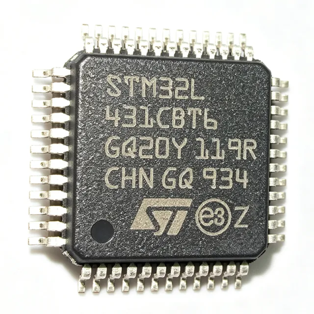
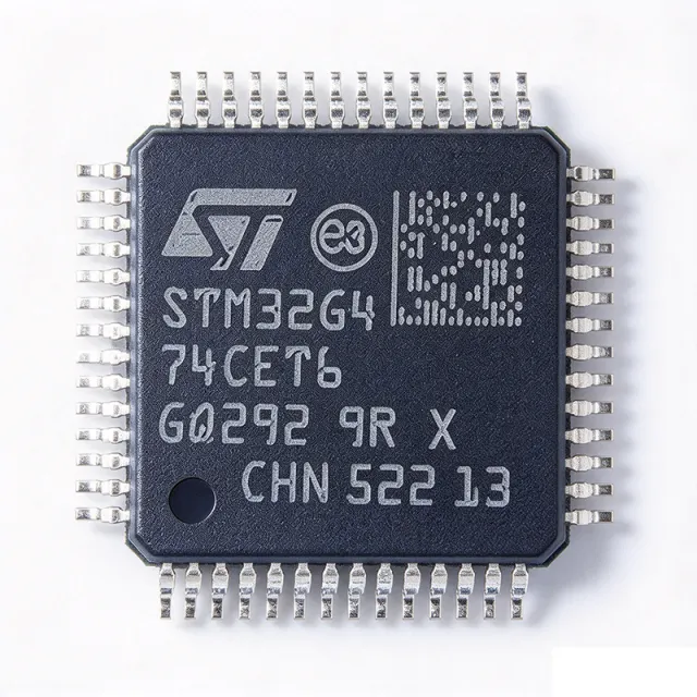
STM32G0B1RET6
STM32G0B1RET6 - 64MHz Cortex-M0+ 512KB MCU | STMicroelectronics
STMicroelectronics STM32G0B1RET6 is an Arm Cortex-M0+ 32-bit RISC microcontroller operating at up to 64 MHz, with 512 KB of Flash memory, 144 KB of RAM, and a 64-pin LQFP 10 x 10 mm package. The device belongs to the STM32G0 mainstream microcontroller family and combines a compact general-purpose MCU with six USART interfaces and embedded security features.
A microcontroller is a programmable system-on-chip that integrates a CPU, memory, peripherals, and communication interfaces on one integrated circuit. Within the semiconductor hierarchy, an MCU is a semiconductor, embedded controller, and general-purpose processing device. The STM32G0 family targets cost-sensitive embedded applications while retaining an Arm ecosystem, efficient real-time execution, and extensive peripheral integration.
The STM32G0B1RET6 provides up to 512 KB of Flash memory with protection, securable areas, two banks, and read-while-write support. It also includes 144 KB of RAM and six USART peripherals. Its Arm Cortex-M0+ core operates at up to 64 MHz, providing useful processing capacity for control loops, human-interface systems, communications, and connected industrial equipment. The 64-pin LQFP package also exposes substantially more I/O than smaller MCU packages.
The two-bank Flash organization supports controlled programming and protection workflows, while the securable area provides a hardware-defined region for isolating sensitive code or data. These capabilities are relevant to firmware security, access-control products, metering equipment, and systems requiring more disciplined code isolation. Exact details such as supply voltage, peripheral current, ADC performance, and package thermal limits are not included in the supplied records and must be confirmed in the manufacturer datasheet.
Typical uses include industrial automation modules, building and access-control terminals, serial gateways, sensor-hub controllers, battery-powered instruments, and human-machine interfaces. The combination of 64 MHz processing, 512 KB Flash, 144 KB RAM, and six USART channels is particularly useful when a design must manage multiple serial endpoints while retaining enough memory for protocol stacks, local data buffering, and application firmware.
Engineers should treat software migration, peripheral mapping, clock configuration, and bootloader compatibility as part of replacement planning. A component having the same package does not by itself prove that firmware is interchangeable. Before substitution, verify the exact pin assignment, power domains, peripheral configuration, pin multiplexing, boot behavior, and errata applicable to the production revision.
This page consolidates the supplied manufacturer and distributor records, verified memory and interface specifications, package information, and a structured comparison of same-family alternatives. It also adds engineering guidance for memory planning, mixed-signal design, and production sourcing while clearly identifying details that still require datasheet confirmation.
طلب عرض سعر
اتصل بنا