المنتجات (20,000+)

W78L365A24PL - 8-Bit 24MHz 64KB MCU | Nuvoton | PLCC-44
W78L365A24PL

W78L365A24PL - 8-Bit 24MHz 64KB MCU | Nuvoton | PLCC-44

Nuvoton Technology Corporation W78L365A24PL is an 8-bit W78 8052-compatible microcontroller with a 24 MHz operating frequency, 64 KB of flash program memory, and a 44-pin PLCC package. It provides 36 I/O pins and 1.25K x 8 bits of RAM, making it suitable for embedded control systems requiring substantial flash storage, moderate I/O density, and a compact leaded-chip carrier footprint. A microcontroller is a programmable integrated circuit that combines a CPU core, memory, timers, serial interfaces, and I/O ports on one device. The W78 family belongs to the broader 8-bit embedded-controller hierarchy, where an instruction-compatible architecture can support legacy 8052 designs while flash memory simplifies firmware updating. The W78L365A24PL is intended for appliances, industrial controllers, instrumentation, and other systems that need deterministic embedded control rather than application-processing performance. The principal device parameters are a 24 MHz clock, 64 KB of flash program memory, 1.25K x 8 bits of RAM, and 36 I/O lines. The suffix identifies the 24 MHz configuration, while the PL package designation identifies the leaded PLCC implementation. Program storage supports firmware of up to 64K x 8 bits, and the 36 available I/O pins permit connections to sensors, switches, displays, actuators, and communication peripherals. The W78 8052-compatible core provides a familiar programming model for engineers maintaining or adapting existing 8051-family equipment. Flash-based program memory can simplify field updates because the firmware can be reprogrammed without replacing the device. Exact instruction-set extensions, interrupt-vector details, timer resources, oscillator options, electrical limits, and temperature ratings should be confirmed in the manufacturer datasheet before a new production design is released. Typical applications include appliance control panels, small industrial controllers, data-acquisition modules, keypad interfaces, LED indicators, motor-control supervisory logic, and embedded instrumentation. The 36 I/O count is especially useful when a design must connect multiple discrete inputs and outputs while retaining a single compact controller package. For designs requiring greater processing speed, memory density, or low-power features, the available silicon should be compared against the system timing and peripheral requirements. PCB planning should account for the PLCC package's J-lead geometry, solder-joint access, and thermal cycling requirements. Confirm the land pattern, pin-1 orientation, exposed-pad arrangement, and recommended reflow profile against the official package drawing. Do not assign signals to the 44 package positions until the complete pin description table has been checked because the visible web results do not provide a verifiable pin-by-pin map. This product page consolidates the identified device specifications, sourcing information, engineering guidance, and strict drop-in replacement analysis. It also distinguishes confirmed electrical facts from parameters that still require direct confirmation from the manufacturer documentation before schematic release, PCB layout, or firmware transfer.

طلب عرض سعر اتصل بنا
W78L516A24PL - 24MHz 8-bit 8052 MCU 64KB Flash | Nuvoton
W78L516A24PL

W78L516A24PL - 24MHz 8-bit 8052 MCU 64KB Flash | Nuvoton

The Nuvoton (formerly Winbond) W78L516A24PL is an 8-bit 8052-compatible microcontroller built around an in-system programmable Flash EPROM architecture, operating at up to 24 MHz with 64 KB of main Flash program memory housed in a 44-pin PLCC package. The part integrates a 4 KB auxiliary Flash loader region that can rewrite the 64 KB main Flash, enabling field firmware updates without an external programmer. An 8-bit microcontroller (MCU) is a single-chip computer that combines a CPU core, program memory, RAM, and peripheral I/O on one die. The W78L516 belongs to the 8051/8052 family - one of the most widely deployed microcontroller architectures globally - and falls within the broader categories of embedded controller, microprocessor, and semiconductor IC. The 8052 instruction set is fully upward-compatible with the original 8051, giving the W78L516 access to a vast ecosystem of compilers, debuggers, and reference code. Key features include 64 KB main Flash plus 4 KB loader Flash, 256 bytes of on-chip RAM, four 8-bit I/O ports, three 16-bit timers/counters, a full-duplex UART, and a six-source interrupt controller. The Flash supports in-application programming via the on-chip loader, removing the need for an external ROM or EPROM. The device operates from a 2.4 V to 5.5 V supply and supports commercial and industrial temperature grades per the W78L516 datasheet. Architecture-wise, the W78L516 uses the standard 8052 machine cycle (12 oscillator clocks per cycle), giving roughly 2 MIPS at the 24 MHz maximum. The dual-Flash layout (main + loader) is the key differentiator over single-Flash 8051 parts, because it lets firmware rewrite itself - a useful capability for remote sensor nodes, industrial controllers, and consumer appliances that may need in-field patches. Typical applications include industrial control boards, smart sensors, motor-control front-ends, security alarm panels, consumer appliances, and legacy 8051 firmware migration projects. Designers commonly pair the W78L516 with Nuvoton W27C512 EEPROMs or low-dropout regulators such as the LM1117. When designing, evaluate whether the 12-clock 8052 core delivers enough throughput; if not, consider an enhanced 8051 such as the Nuvoton N76E003 or a 32-bit MCU. Confirm Flash endurance and retention figures against the application's write-cycle budget, and budget for the loader region in code-size calculations.

طلب عرض سعر اتصل بنا
W78L801A24DL - 8-bit 8051 24MHz 40-DIP | Winbond
W78L801A24DL

W78L801A24DL - 8-bit 8051 24MHz 40-DIP | Winbond

The Winbond Electronics W78L801A24DL is an 8-bit 8051-compatible microcontroller with 4KB of mask ROM, 256 bytes of RAM, 32 I/O pins, a 24MHz clock rating, and a 40-pin DIP package. Its core role is compact embedded control for cost-sensitive products that require reliable logic execution, serial communication, timing, and discrete I/O handling without a large flash-memory footprint. A microcontroller is a semiconductor device that integrates a CPU core, program memory, data memory, I/O ports, timers, and communication peripherals into one integrated circuit. The W78L801A24DL belongs to the 8-bit MCU family and uses an 8051-compatible instruction set, making it suitable for legacy-compatible control logic, compact instrumentation, appliance interfaces, and small embedded systems. Its mask-programmed ROM is appropriate for high-volume products where firmware is fixed during manufacturing. The principal device characteristics include 4KB of program memory organized as 4K x 8, 256 x 8 bits of RAM, 32 I/O lines, and operation up to 24MHz. The device is identified in the 40-DIP package, providing through-hole assembly compatibility and straightforward prototyping. The W78L801 family also supports software-selectable idle and power-down operating modes. In idle mode, processor clock operation stops while selected peripheral functions can continue; power-down mode stops the crystal oscillator for lower power consumption. The W78L801A24DL is appropriate for controllers that need a modest code space and deterministic peripheral handling rather than high-volume flash storage, complex operating systems, or high-speed connectivity. Its 8051-compatible architecture can simplify migration from older 8051 designs. The 24MHz upper speed rating supports faster instruction throughput than many traditional 8-bit designs, although real timing must be checked against the operating voltage and device-specific limits. Typical implementations include small appliance controllers, sensor-interface modules, industrial control panels, lighting-control boards, simple serial-interface equipment, and legacy peripheral controllers. The 32 available I/O lines provide useful connectivity for buttons, indicators, relays, displays, and external logic, while on-chip timers and communication functions reduce the need for additional support components. Design with the 40-pin footprint on the PCB and follow the manufacturer pin-description table when assigning signals. Decoupling must be placed close to the supply pins, oscillator components must follow the recommended layout, and unused inputs should be configured to avoid unintended current or state transitions. The fixed mask ROM also means firmware changes normally require a different programming arrangement or a device revision, making definition-time software locking essential. This page combines the core electrical and packaging characteristics, practical integration guidance, application fit, and replacement constraints. It also distinguishes the W78L801A24DL from merely similar 8051-class devices, because equal package size and clock rating alone do not establish pin-to-pin compatibility.

طلب عرض سعر اتصل بنا
W78L801A24FL - 8-Bit 24MHz 44-Pin Microcontroller | Nuvoton
W78L801A24FL

W78L801A24FL - 8-Bit 24MHz 44-Pin Microcontroller | Nuvoton

Nuvoton W78L801A24FL is an 8-bit 8051-compatible microcontroller rated for operation from 1.8 V to 5.5 V, with a 24 MHz clock and 4 KB of MROM in a 44-pin QFP package. The W78L801A24FL is positioned for compact embedded-control designs that require a conventional 8051 architecture, low-voltage operation, and a moderate pin count. An 8051 microcontroller is a small, instruction-set-oriented embedded controller used to supervise sensors, switches, displays, communication peripherals, and actuator logic. The 8051 family combines a CPU core, program memory, data memory, timers, serial interfaces, and GPIO functions in one integrated circuit. Because the W78L801A24FL belongs to this established embedded-control category, it is useful for designs that value compact instruction execution, deterministic peripheral control, and broad software familiarity. The device is identified as an 8-bit MCU with 4 KB MROM and a maximum clock frequency of 24 MHz. Its stated operating voltage range of 1.8 V to 5.5 V supports both low-voltage and conventional 5 V system rails. One distributor listing also identifies the family as 51-series, reinforcing its 8051-compatible positioning. The package is specified as QFP-44 in a 10 mm by 10 mm surface-mount format, while another listing describes the package as 44-BQFP. Typical embedded uses include appliance controls, small industrial modules, keypads, LED indicators, sensor-conditioning front ends, programmable logic controllers, and compact consumer products. The 24 MHz operating rate supports timing-intensive control tasks, while the 8-bit architecture is most appropriate when the application is dominated by GPIO, timers, serial communication, and simple state-machine control rather than intensive arithmetic or large graphical interfaces. When laying out a W78L801A24FL board, use the manufacturer pin description table to assign every signal and preserve the exposed-pad, power, ground, clock, reset, and programming connections. Confirm the oscillator frequency, decoupling requirements, and programming interface against the manufacturer datasheet before releasing the PCB. This page combines the available device characteristics with practical application guidance, package information, sourcing support, and an honest comparison framework for engineers evaluating this 8051-family MCU.

طلب عرض سعر اتصل بنا
W78L801A24LL 8-Bit 8051 MCU, 4KB ROM, 48-LQFP | Nuvoton
W78L801A24LL

W78L801A24LL 8-Bit 8051 MCU, 4KB ROM, 48-LQFP | Nuvoton

The Nuvoton W78L801A24LL is an 8-bit 8051-family microcontroller with 4KB of mask ROM, a 48-pin LQFP package measuring 7 mm by 7 mm, and an operating voltage range listed as 2.5 V, 3.3 V, or 5 V. It is designed for compact embedded-control designs that require a conventional 8051 architecture, low pin count, and direct peripheral integration rather than a high-performance application processor. A microcontroller is a semiconductor device that integrates a CPU core, program memory, data memory, I/O ports, and peripherals into one package. The W78L801A24LL belongs to the 8051 microcontroller family, which is a CISC-based embedded-processing platform used in appliances, industrial controllers, access equipment, meters, and small automation systems. Its 4KB mask ROM provides a fixed program area for embedded control logic, while the 48-pin LQFP provides a substantial number of external signal connections for digital interfaces and control functions. The key identifiable specifications are the 8-bit CPU architecture, 4KB MROM, 48-pin LQFP package, and 2.5 V, 3.3 V, or 5 V supply options. A distributor listing also identifies the device as an active Nuvoton part and classifies it as a QFP-48 package. The product is associated with an operating-frequency entry of 24 MHz in one listing and 20 MHz in another; the applicable maximum clock for the exact ordering code must therefore be confirmed against the manufacturer datasheet before clock-tree or timing design is finalized. Typical embedded uses include keypad-controlled industrial panels, compact appliance controllers, fan and pump sequencers, digital instrumentation, LED status and drive systems, and small peripheral-control boards. The 8051 instruction set is appropriate when the application favors a mature software ecosystem and deterministic peripheral control over a larger CPU core, larger RAM, high-speed connectivity, or extensive analog conversion resources. Design planning should begin with the manufacturer pin-description table, oscillator requirements, reset behavior, I/O ratings, and memory map. Confirm the exact clock limit, RAM capacity, peripheral set, input thresholds, and output-drive limits before finalizing the schematic. A 48-pin LQFP also requires a land pattern that matches the manufacturer's package drawing, including exposed-pad and thermal-copper requirements where applicable. This product page consolidates the verified package, memory, architecture, supply-voltage, lifecycle, and sourcing information into an engineering-oriented reference. It also distinguishes confirmed device attributes from parameters that require direct datasheet verification and avoids presenting generic cross-reference listings as guaranteed drop-in replacements.

طلب عرض سعر اتصل بنا
W78L801A24PL - 24MHz 8-Bit 8051 MCU with 4KB ROM | Nuvoton
W78L801A24PL

W78L801A24PL - 24MHz 8-Bit 8051 MCU with 4KB ROM | Nuvoton

Nuvoton Technology Corporation W78L801A24PL is an 8-bit 8051-compatible microcontroller with a 24 MHz clock, 4 KB mask ROM organized as 4K x 8 bits, and a 44-LCC J-lead package. Its operating voltage range is 1.8 V to 5.5 V, making it suitable for embedded control, monitoring, and compact industrial or consumer systems. The device also provides 256 bytes of data memory and software-selectable idle and power-down operating modes for reduced power consumption. An 8-bit microcontroller is a programmable semiconductor that integrates a processor core, program memory, data memory, and peripherals into one device. The W78L801 belongs to the 8051 family, a widely used embedded-control architecture also known as an MCS-51 microcontroller. Its 4 KB mask ROM stores the fixed firmware program, while its 256-byte RAM supports variables, stack operations, and intermediate working data. Applications generally center on sequential control logic, sensor acquisition, keypad or display control, and communication interfaces. The principal operating characteristics include a maximum clock frequency of 24 MHz, an 8-bit processing architecture, 4 KB of mask-programmable ROM, and a 1.8 V to 5.5 V supply range. Two software-controlled power modes help conserve energy. Idle mode stops the processor clock while allowing supported peripheral operations to continue, whereas power-down mode stops the crystal oscillator for minimum power consumption. The external clock may also be stopped without affecting processor state according to the W78L801 datasheet. The W78L801A24PL combines conventional 8051 instruction-set compatibility with a surface-mount LCC implementation. The PL suffix denotes the 44-LCC J-lead package shown in product documentation. Its masked-program architecture is appropriate for high-volume products in which firmware is finalized before production. Because the program memory is mask ROM rather than user-programmable flash, firmware changes normally require a different programmed device rather than an in-circuit update. Typical uses include industrial controllers, appliance-control boards, instrumentation modules, building equipment, and compact embedded systems that benefit from the low-power operating modes. The 24 MHz clock provides additional processing headroom for time-sensitive control tasks, while the 8051 instruction set supports a compact software ecosystem and established development methods. System-level suitability depends on the selected external clock, memory organization, and peripheral requirements described in the datasheet. Designers should verify the exact pin functions, oscillator connections, reset behavior, and available I/O assignments against the manufacturer pin-description table before laying out a PCB. Decoupling, clock stability, exposed programming considerations, and supply sequencing also require normal mixed-signal layout practices. Because this package is a leaded LCC rather than a fine-pitch bare die, assembly planning should account for its 44 J-leads. This page combines the manufacturer-oriented device description with verified product parameters, application guidance, design cautions, and a transparent comparison of what the available technical information establishes. It helps engineers identify whether the W78L801A24PL architecture, memory configuration, clock rate, voltage range, and package align with a new embedded-control design.

طلب عرض سعر اتصل بنا
W78L812A24DL - 8-Bit 24MHz 8051 MCU | Nuvoton
W78L812A24DL

W78L812A24DL - 8-Bit 24MHz 8051 MCU | Nuvoton

Nuvoton Technology Corporation W78L812A24DL is an 8-bit 8051-compatible microcontroller with 24 MHz clocking, 8 KB of flash program memory, 32 I/O pins, and a 40-pin DIP package. Its 2.4 V to 5.5 V operating range supports low-voltage embedded control systems requiring an 8-bit processor with integrated flash memory. An 8-bit microcontroller is a programmable semiconductor designed for embedded control. The W78 series combines an 8051-compatible core, program memory, data memory, and peripherals in one device. Within the embedded-control hierarchy, the W78L812A24DL is an MCU, or microcontroller unit, intended to execute firmware that monitors inputs and controls outputs in appliances, industrial equipment, and compact automation systems. Key features include 8 KB of flash program memory organized as 8K x 8, a maximum clock frequency of 24 MHz, and 32 I/O lines. EBI/EMI and UART/USART interfaces provide external-memory and serial-communication options, while integrated LED and watchdog-timer functions support status indication and system supervision. The stated 2.4 V to 5.5 V operating-voltage range also supports compatibility with common embedded power rails. The device uses an 8-bit data path and an 8051-compatible processor core. Its flash memory permits firmware to be programmed and updated without an external program-memory device, simplifying both production and maintenance. The 40-DIP mechanical package facilitates through-hole assembly and prototyping, although its larger footprint is less suitable for compact surface-mount products than smaller microcontroller packages. Typical applications include appliance controllers, LED status and sequencing systems, industrial control panels, small motor or relay interfaces, serial-connected embedded modules, and educational 8051 platforms. Designers should confirm RAM capacity, detailed timer and peripheral assignments, clock behavior, and all electrical limits against the manufacturer datasheet before creating a production PCB. For a new design, verify the 40-pin footprint, oscillator requirements, reset behavior, and available I/O functions. The DIP package simplifies breadboard and through-hole prototypes, but a high-density production design may require a different package variant and a corresponding PCB redesign. This product page consolidates the confirmed operating specifications, interface capabilities, application guidance, sourcing path, and drop-in-replacement status for engineers evaluating the W78L812A24DL.

طلب عرض سعر اتصل بنا
W78L812A24FL - 8-Bit 24MHz 8051 Flash MCU | Nuvoton
W78L812A24FL

W78L812A24FL - 8-Bit 24MHz 8051 Flash MCU | Nuvoton

The Nuvoton W78L812A24FL is an 8-bit 8051-compatible Flash microcontroller with an operating clock of 24 MHz, 8 KB of Flash EPROM, 256 bytes of RAM, and a 44-pin QFP package. It operates from 2.4 V to 5.5 V and integrates four 8-bit bidirectional I/O ports, an additional 5-bit P4 port, three 16-bit timer/counters, a hardware watchdog timer, and a serial port. An 8051-compatible microcontroller is a compact embedded-control device built around the classic MCS-51 instruction set. Microcontrollers combine a CPU, program memory, data memory, timers, serial communication, and digital I/O on one integrated circuit. This integration allows control systems to monitor inputs, execute embedded software, operate timers, and exchange serial data without requiring a separate processor and supporting components. The W78L812A24FL combines 8 KB of Flash EPROM with 256 bytes of RAM, providing useful program storage for compact embedded applications. Its four 8-bit ports and dedicated P4 port offer multiple digital interfaces, while the three 16-bit timer/counters support periodic events, timing measurements, and waveform generation. The hardware watchdog timer adds an independent mechanism for recovering from stalled program execution. The 24 MHz operating frequency provides a higher instruction-processing rate than lower-frequency members of the same device family while retaining standard 8051 instruction-set compatibility. This makes the device suitable for designs based on established 8051 firmware, industrial controllers, compact instruments, appliance controls, and general-purpose embedded products requiring deterministic digital I/O. Typical uses include motor and actuator sequencing, temperature-instrument signal acquisition, keypad interfaces, LED status panels, programmable timers, and serial-connected control modules. The 2.4 V to 5.5 V operating range supports both lower-voltage and conventional 5 V designs, allowing system designers to choose the MCU around the power architecture of the finished product. PCB design should preserve stable supply decoupling near the power pins and route the oscillator, reset, and high-speed signals according to the manufacturer reference layout. Because the device offers limited RAM, firmware should use the available data memory carefully. Firmware development also benefits from 8051-compatible tools because the instruction set remains compatible with the standard 8051 architecture. This page organizes the principal electrical, memory, peripheral, package, and application characteristics of the W78L812A24FL. It also identifies same-family alternatives and explains the practical distinctions that matter when evaluating an 8051-compatible control IC for an embedded product.

طلب عرض سعر اتصل بنا
W78L812A24PL - 8-bit 8051 MCU, 8KB Flash, 24MHz | Nuvoton
W78L812A24PL

W78L812A24PL - 8-bit 8051 MCU, 8KB Flash, 24MHz | Nuvoton

The Nuvoton Technology Corporation W78L812A24PL is an 8-bit microcontroller with a fully 8051-compatible instruction set, an 8 KB Flash EPROM program memory, 256 bytes of RAM and a 24 MHz operating frequency, housed in a 44-pin PLCC (PL) package with a 2.4 V to 5.5 V supply range. An 8-bit MCU is the simplest tier of the microcontroller hierarchy: MCU -> 8-bit microcontroller -> 8051 core -> embedded control IC. The W78L812 belongs to the 8051 family of single-chip computers, combining a CPU core, program memory, data memory and peripherals on one die. Because the instruction set is compatible with the standard 8051, existing 8051 assembler, C compiler and bootloader tooling can be reused without architectural changes. Key features include 8 KB of Flash EPROM instead of masked ROM, which allows field re-programming and simplifies product revisions. The device carries 256 bytes of internal RAM plus a 256-byte XRAM area, four 8-bit bi-directional bit-addressable I/O ports (P0 through P3), an additional 5-bit port P4, and three 16-bit timer/counter blocks with interrupt support for timing, pulse counting and periodic event generation. A 24 MHz oscillator gives roughly ten times the execution rate of a classic 12 MHz 8051. Because the instruction set, memory map and port structure follow the established 8051 convention, the W78L812A24PL is a natural fit for cost-sensitive embedded controllers that must run existing 8051 code. The wide 2.4 V to 5.5 V supply range allows direct operation from unregulated industrial rails, 3.3 V systems or rechargeable cells after regulation. Typical applications include smart appliances, small motor controllers, security keypads, industrial sequencers, LED lighting controllers and low-cost data acquisition front ends. Its PLCC package is a strong argument for designs that expect manual soldering or socketed prototyping rather than fully automated SMT assembly. When designing around this device, remember that Flash EPROM programming requires a dedicated programmer, and that the 44-PLCC footprint is not the same as the 40-pin DIP variant of the same family. Confirm the pinout and package drawing from the manufacturer datasheet before laying out the board, and keep decoupling close to the supply pins.

طلب عرض سعر اتصل بنا
W79E217AFG - 8-bit 8051 MCU 64KB Flash 33MHz PQFP-100 | Nuvoton
W79E217AFG

W79E217AFG - 8-bit 8051 MCU 64KB Flash 33MHz PQFP-100 | Nuvoton

The Nuvoton Technology Corporation W79E217AFG is an 8-bit 8051/8052-compatible microcontroller (MCU) with a redesigned processor core that eliminates wasted clock and memory cycles, delivering up to 33 MHz core frequency and integrating 64 KB (64K x 8) of on-chip Flash program memory. Housed in a 100-pin PQFP package, it operates from a single 5 V supply (with operating voltage range per datasheet) and is positioned as a drop-in upgrade for legacy 80C51/80C52 designs that need more code space, more I/O, and embedded Flash in-system programming (ISP). A microcontroller (MCU) is a single-chip computer containing a CPU core, program memory (ROM/Flash), data memory (RAM), and peripherals such as timers, UARTs, ADC, GPIO, and interrupt controllers. The 8051 family is the most widely deployed 8-bit MCU platform in history; it sits within the broader taxonomy: 8051 -> 8-bit MCU -> microcontroller -> embedded processor -> semiconductor. The W79E217AFG belongs to Nuvoton's W79 series of industrial-grade, Flash-based 8051 derivatives aimed at motor control, instrumentation, and human-machine interface (HMI) applications. Key features of the W79E217AFG include the 33 MHz single-cycle enhanced 8052 core, 64 KB Flash, 256 + 1 KB on-chip SRAM, four 8-bit I/O ports (P0-P3), three 16-bit timers, two full-duplex UARTs, an 8-channel 10-bit ADC, an on-chip oscillator, watchdog timer, power-on reset, and brown-out detector. Industrial temperature range (-40 °C to +85 °C), PQFP-100 package with 84 usable I/O lines, and ISP via UART make it well-suited for embedded designs. Architecturally, Nuvoton re-engineered the classic 8051 pipeline to remove the original 12-clock-per-machine-cycle penalty, allowing most instructions to complete in one clock. This typically yields 2x-3x throughput vs. legacy 80C51 at the same crystal frequency, while preserving binary compatibility with standard 8051 code, assemblers, and Keil C51 toolchains. The integrated 64 KB Flash also enables field updates without external EPROM. Typical applications include industrial motor drives, AC/DC inverter controls, induction cooker controllers, smart appliance HMI panels, security alarm panels, and other 8051-based legacy designs that need to migrate from ROM/EPROM to Flash. The wide operating temperature range and large PQFP package with abundant I/O make it appropriate for human-interface boards that drive LEDs, keypads, and character/graphic LCDs. When designing with this part, ensure your ISP tool is configured for the W79E217 family boot-loader entry mode and that decoupling is placed close to the analog AVSS/AVDD pins if the 10-bit ADC is used. This page synthesizes distributor pricing, drop-in alternatives, and practical design notes not found on the manufacturer datasheet alone.

طلب عرض سعر اتصل بنا
W79E352AFG - 8-bit 8051 MCU, 24MHz, 8KB Flash, 44-QFP | Nuvoton
W79E352AFG

W79E352AFG - 8-bit 8051 MCU, 24MHz, 8KB Flash, 44-QFP | Nuvoton

The Nuvoton W79E352AFG is an 8-bit 8051-family microcontroller core running up to 24 MHz, integrating 8 KB of on-chip Flash program memory and 256 bytes of SRAM, supplied in a 44-pin QFP package. It is built around an industry-standard 8051 instruction set, providing full compatibility with the MCS-51 toolchain, Keil C51, and SDCC while adding modern peripherals such as PWM, WDT, brown-out reset, low-voltage detect (LVD), and power-on reset. An 8-bit microcontroller (MCU) is a single-chip computer that integrates a CPU, program memory (ROM/Flash), data memory (RAM), and I/O peripherals into one package. The 8051 architecture, originally introduced by Intel in 1980 and now maintained by Nuvoton and others, sits within the broader hierarchy: microcontroller -> embedded processor -> digital IC -> semiconductor. The W79E352AFG belongs to Nuvoton's W79 series, optimized for cost-sensitive industrial control, home appliance, and motor drive front-ends. Key features of the W79E352AFG include up to 36 general-purpose I/O pins, multiple communication interfaces (EBI/EMI, I2C, UART/USART), four 16-bit timer/counters, hardware PWM channels, and an in-system programmable (ISP) Flash that enables firmware upgrades without removing the device from the board. Operating voltage spans 2.4 V to 5.5 V, supporting both 3.3 V and 5 V system designs with a single device. Technically, the part uses a single-cycle 8051 core that executes most instructions in 1 to 4 clocks (versus 12 in the original 8051), yielding roughly 4x to 12x higher effective MIPS than legacy designs. The integrated 4 KB auxiliary Flash area allows bootloader/ISP separation from the application code region. On-chip RC oscillator options reduce external BOM, and configurable GPIO drive strength simplifies interface to relays, MOSFETs, or 5 V peripheral logic. Typical applications include BLDC and stepper motor control (using the PWM and timer modules), home appliances (washing machines, induction cookers, microwave ovens), industrial control boards, low-end sensor hubs, and replacement of legacy 8051 designs where pin compatibility, code compatibility, and an upgrade path to ISP Flash are required. When designing in this part, reserve pin 30 (RST) for an external reset network and ensure the VDD-to-VSS decoupling is placed within 5 mm of the package. Designers moving from older Nuvoton N79E352ADG (44-DIP) parts can reuse existing firmware because the W79E352AFG shares the same SFR map. This page synthesizes distributor pricing, drop-in alternatives, package diagrams, and practical design notes that complement the official Nuvoton datasheet for engineers migrating legacy 8051 designs or evaluating the W79 series for new industrial and appliance projects.

طلب عرض سعر اتصل بنا
W79E8213AKG - 8-bit 8051 MCU, 4KB Flash, 20MHz, 20-DIP | Nuvoton
W79E8213AKG

W79E8213AKG - 8-bit 8051 MCU, 4KB Flash, 20MHz, 20-DIP | Nuvoton

The Nuvoton W79E8213AKG is an 8-bit 4T-8051 microcontroller with 4KB of in-system programmable Flash EPROM, executing one instruction per clock cycle at up to 20MHz and housed in a 20-pin PDIP (DIP-20) through-hole package. It provides 128 bytes of on-chip RAM, brown-out detection, and an integrated 4-channel 10-bit ADC, targeting cost-sensitive industrial and consumer control applications where a mature 8051 core simplifies firmware reuse. An 8-bit 8051 microcontroller is a small single-chip computer based on the original Intel MCS-51 architecture, combining an 8-bit CPU, program memory, data RAM, and peripherals on a single silicon die. The 8051 family is widely classified as an MCU (microcontroller unit) within the broader category of microcontrollers, embedded processors, and finally semiconductors. Nuvoton's W79 series extends the legacy 8051 footprint with modern process technology, larger Flash densities, and ICP (In-Circuit Programming) capability for field-reprogrammability without removing the part from the board. Key features include 4KB (4K x 8) Flash program memory that supports both hardware writer and ICP modes, 128 bytes of on-chip SRAM, an operating frequency up to 20MHz, internal watchdog timer and brown-out reset for robust field operation, and a 20-pin DIP form factor that fits legacy through-hole PCB designs. The device runs across the industrial -40C to +85C temperature range, supports standard 8051 peripherals (UART, timers, GPIO), and integrates an ADC for mixed-signal sensing. At the silicon level, the W79E8213 uses a 4T (four-clock-per-machine-cycle) 8051 core, providing single-cycle instruction execution that delivers up to four times the throughput of legacy 12T 8051 derivatives at the same clock rate. The mixed program/data Flash architecture is partitioned as 4KB code space at the base address, with hardware lock bits available to protect intellectual property against unauthorized readout. Power management includes idle and power-down modes that drop supply current to microampere levels for battery-backed installations. Typical applications include home appliance controls such as rice cookers and washing machines, white goods and HVAC blower control modules, battery chargers, LED lighting controllers, security keypads, and small-format industrial control boards. The DIP-20 package and 8051 instruction set also make the W79E8213AKG a drop-in upgrade for legacy 8051 designs that need more Flash without requiring PCB rework. When designing with the W79E8213AKG, provide a 0.1uF decoupling capacitor as close as possible to VDD and a bulk capacitor on the reset pin if external reset components are used. For ISP/ICP, three of the device's GPIO pins double as the programming interface and must not be permanently pulled to a logic level during the in-circuit programming sequence. Operating voltage is typically 5V with tolerance for 3V to 5.5V operation depending on frequency. This page synthesizes distributor stock levels, parametric alternatives, ICP programming notes, and 8051 architecture context that supplement the manufacturer datasheet and help engineers select the right drop-in replacement when the W79E8213AKG reaches end-of-life.

طلب عرض سعر اتصل بنا
W79E825AW - 8-Bit MCU, 16KB ISP Flash, 18 I/O Ports | Nuvoton
W79E825AW

W79E825AW - 8-Bit MCU, 16KB ISP Flash, 18 I/O Ports | Nuvoton

The Nuvoton W79E825AW (formerly Winbond W79E825A family) is an 8-bit CMOS microcontroller built around a high-speed 4T (four-clock-per-instruction) core architecture, providing 16 KB of in-system programmable (ISP) Flash program memory, 256 bytes of on-chip RAM, and 256 bytes of data-flash NVM. The device integrates 18 multi-function I/O pins, two 16-bit timer/counters, 13 interrupt sources arranged in four priority levels, one Enhanced full-duplex UART, one I2C bus interface, a programmable Watchdog Timer, four channels of 10-bit PWM, and a 4-channel multiplexed 10-bit A/D converter. According to the manufacturer datasheet, the on-chip oscillator and clock circuitry eliminate the need for an external crystal on many designs, while a selectable instruction cycle architecture balances throughput and power consumption. The W79E825AW shares its fundamental die with the broader W79E82xA family, and is offered in the 'AW' suffix package code. A microcontroller (MCU) is a single-chip computer that integrates a CPU, non-volatile program memory, volatile RAM, and peripheral interfaces into one package; 8-bit MCUs such as the W79E825AW remain widely used in cost-sensitive embedded designs where the processing workload (sensing, key handling, simple state machines, motor pulse trains) fits comfortably within an 8-bit data path. Within the broader semiconductor taxonomy, an MCU belongs to the microcontrollers sub-category of Integrated Circuits, sitting above Logic ICs and beneath microprocessors in capability. The 4T core architecture positions the W79E825AW for one-instruction-per-four-clock operation, providing up to several MIPS per MHz depending on the selected clock source. Key features of the W79E825AW include ISP Flash that supports in-application firmware updates without removing the part from the board, a configurable 4-/2-channel 10-bit PWM block for motor or LED control, a 10-bit ADC that can be routed to multiple I/O pins, and a Brown-out / Watchdog combination for unsupervised recovery from power or code faults. The four-level interrupt controller lets time-critical events preempt background tasks, and the Enhanced UART supports 9-bit address-mode communications for RS-485 multi-drop networks. Typical applications include white-goods control boards, low-end motor drives, simple sensor hubs, IR remote transceivers, and consumer-electronic user-interface modules. The 18 I/O budget covers keypad scanning, LED driving, and small display interfaces without external expanders. When designing with this part, leave at least one UART accessible as a serial debug / ISP window and verify the ISP entry sequence against the In-System Programming section of the manufacturer datasheet to avoid lock-out conditions.

طلب عرض سعر اتصل بنا
W79E9781AKG - 8-bit MCU 64KB Flash | Nuvoton | Industrial
W79E9781AKG

W79E9781AKG - 8-bit MCU 64KB Flash | Nuvoton | Industrial

The Nuvoton W79E9781AKG is an 8-bit Turbo 51-compatible microcontroller with 64 KB of in-system programmable Flash, 1.25 KB SRAM, and a wide operating voltage range, packaged in a 128-pin LQFP. It integrates a 10-bit ADC, four 16-bit timers, a watchdog timer, a full-duplex hardware UART, an I2C/SPI master interface, and a built-in brown-out detector for industrial-grade reliability. An 8-bit microcontroller (MCU) is a microprocessor-on-a-chip that integrates a CPU, program memory, data RAM, and peripherals into a single IC. The 8-bit architecture is optimized for cost-sensitive, low-power, deterministic control tasks; in the system hierarchy an MCU sits between discrete logic ICs and 32-bit microprocessors, providing firmware-driven I/O handling, sensor interfacing, and protocol conversion. Nuvoton's W79 family extends the legacy 8051 instruction set with Turbo-MCU enhancements, doubling the standard clock-per-instruction cycle for higher throughput at the same crystal frequency. Key features include 64 KB of in-system programmable (ISP) Flash allowing field firmware updates via UART, an operating voltage range of 2.4V to 5.5V that supports both 3.3V and 5V rails, and an industrial-grade operating temperature of -40C to +85C. The on-chip 10-bit ADC provides up to 8 analog input channels, while the four 16-bit timer/counters support PWM generation, capture, and event counting. A dedicated hardware watchdog and brown-out reset circuit protect against code lockup and unstable supplies. The W79E9781AKG uses the standard 8051 instruction set with Nuvoton Turbo-MCU extensions, allowing one machine cycle per clock rather than the original 12, while preserving binary compatibility with legacy 8051 firmware. The device's ISP mechanism boots from a ROM-resident bootloader that re-programs the Flash via the UART pins, eliminating external programming hardware during prototyping and field service. Typical applications include industrial control panels, home appliance main boards, motor control BLDC drivers, smart meter data concentrators, and point-of-sale terminals. The integrated ADC, timers, and UART let designers replace multiple discrete components with a single chip, shrinking BOM cost and PCB area. When designing with this device, plan ISP access by routing the UART pins to a header or optocoupler-isolated connector. Use the brown-out detector level matched to the lowest reliable rail voltage (typically 2.7V for 3.3V systems) to prevent Flash corruption during power-down events. This page consolidates distributor pricing, package-level drop-in alternatives, and engineering design notes that go beyond the manufacturer datasheet, supporting faster component selection and risk-aware substitution decisions.

طلب عرض سعر اتصل بنا
W83L951ADG - Mobile Keyboard Embedded Controller | Winbond
W83L951ADG

W83L951ADG - Mobile Keyboard Embedded Controller | Winbond

The Winbond W83L951ADG is a CMOS mobile keyboard and embedded controller fabricated in a 128-pin LQFP (PQFP128) surface-mount package, integrating an 8051-compatible microcontroller core with keyboard scanning, embedded controller, and system management functions for notebook and mobile computing platforms. It was originally produced by Winbond Electronics Corporation, whose embedded controller product line later transferred to Nuvoton Technology, which is why the same MPN appears under both Winbond and Nuvoton branding in distributor catalogs. An embedded controller (EC) is a specialized microcontroller in the power-management hierarchy of a computer system: it is a dedicated, always-on processor that supervises the keyboard matrix, power sequencing, battery charging supervision, thermal sensing, and low-level I/O even while the main CPU is asleep or off. In laptop and mobile designs the EC is the first silicon to wake and the last to sleep, making its firmware and electrical behavior critical to system reliability. Key features of the W83L951ADG include the 8051-derived instruction-set core with embedded firmware memory, an integrated keyboard controller (KBC) compatible with legacy PC/AT keyboard and PS/2 interfaces, general-purpose I/O for board-level control, and low-power CMOS operation suited to battery-powered systems. The device communicates with the host chipset over an LPC (Low Pin Count) style interface used in legacy EC architectures, allowing ACPI-compliant power management event handling. Architecturally, the part follows the classic Winbond/Nuvoton EC family: a single-chip design combining the CPU, program memory, RAM, keyboard matrix scanner, host interface, timers, and GPIO banks, minimizing external component count in dense mobile motherboards. The LQFP-128 package with 0.4 mm lead pitch provides the pin count needed for large keyboard matrix scanning plus numerous GPIO without a larger footprint. Typical applications include laptop and notebook keyboard controllers, embedded system management in x86 mobile platforms, tablet and portable device keyboard scanning, and industrial legacy designs that require PC/AT-compatible KBC functionality. Design consideration: because this device is long past active production, verify remaining authorized stock and confirm firmware compatibility before committing it to a new build; legacy designs should plan a migration path to current Nuvoton EC families. This page synthesizes distributor sourcing data, datasheet availability, drop-in variant information, and practical obsolescence guidance not consolidated in the manufacturer datasheet.

طلب عرض سعر اتصل بنا
WPC8763LDG - Embedded Controller IC QFP-128 | Winbond
WPC8763LDG

WPC8763LDG - Embedded Controller IC QFP-128 | Winbond

The Winbond Electronics WPC8763LDG is a specialized embedded controller (EC) integrated circuit supplied in a 128-pin QFP surface-mount package, designed primarily for notebook PC and mobile-system platform management applications such as keyboard scanning, power sequencing supervision, and thermal/fan control. An embedded controller is a specialized microcontroller that operates semi-independently of the host CPU to manage low-level platform functions. In the PC system hierarchy, the EC sits below the main CPU and chipset (PCH) as a power-management IC tier: it handles keyboard matrix scanning, battery charging supervision, thermal monitoring, fan speed control, and lid/power-button events, typically following Intel or AMD platform EC firmware specifications such as those used with ACPI and eSPI/KBC interfaces. The WPC8763LDG belongs to Winbond's WPC876x family of embedded controllers, which integrates an 8-bit or proprietary MCU core with on-chip flash/ROM program memory, keyboard controller (KBC) logic, GPIO, PWM channels for fan control, and ADC inputs for thermal and voltage monitoring. Key differentiating features of this family include the high GPIO count required for notebook keyboard matrices, integrated PWM fan controllers that reduce external component count, and low standby power consumption for battery-operated systems. The 128-pin QFP package provides sufficient I/O for a full notebook EC implementation on a single chip. Architecturally, EC devices like the WPC8763LDG combine a low-power MCU core, a shared RAM region, dedicated peripheral blocks (PS/2 keyboard interface, SMBus/I2C masters for battery and thermal IC communication, pulse-width modulators, and watchdog timers), and boot ROM. Firmware executes from internal non-volatile memory, and the EC communicates with the chipset over LPC or eSPI buses depending on platform generation. Typical applications include laptop and notebook motherboard EC functions, keyboard/mouse controller emulation (PS/2 KBC/Mouse), battery charging management in coordination with a charger IC, thermal and acoustic (fan) management, and general-purpose GPIO expansion in portable and industrial embedded systems. A key design consideration is firmware compatibility: the EC must run BIOS-coordinated firmware, so replacing this device requires both hardware pin compatibility and firmware/toolchain support - verify code image compatibility before any substitution. This page synthesizes distributor stock and pricing data, package information, and sourcing guidance not consolidated in the manufacturer's public datasheet listing.

طلب عرض سعر اتصل بنا
XC2287M104F80LRABKXUMA1 - 16/32-Bit 80MHz 832KB Flash MCU | Infineon
XC2287M104F80LRABKXUMA1

XC2287M104F80LRABKXUMA1 - 16/32-Bit 80MHz 832KB Flash MCU | Infineon

The Infineon XC2287M104F80LRABKXUMA1 is a 16/32-bit C166SV2 XC22xxM family microcontroller integrating a CISC/DSP/RISC processing core running at 80 MHz with 832 KB of on-chip Flash and 58 KB RAM, supplied in a 144-pin PG-LQFP-144-4 package with exposed pad. It targets automotive and industrial powertrain, body, and chassis applications requiring deterministic real-time response combined with DSP-grade signal processing throughput on a single die. A microcontroller (MCU) is a single-chip processing subsystem that integrates a CPU core, program and data memory (Flash, ROM, RAM), peripheral interfaces (ADC, timers, communication buses), and power management. Within the broader semiconductor taxonomy, MCUs sit inside Embedded Processors and Controllers, alongside microprocessors (MPUs) and system-on-chips (SoCs); they are typically selected over MPUs when deterministic latency, low power, and tight BOM integration matter more than raw application-processor performance. The C166S V2 core inherits the classic C166 instruction set with DSP extensions and RISC-like single-cycle execution, placing this part in the legacy 16-bit automotive MCU segment alongside derivatives such as the XC2764X and XC2336D families. Key features of the XC2287M104F80LRABKXUMA1 include 832 KB program Flash, 58 KB SRAM, an on-chip 10-bit ADC with up to 118 channels per the JLCPCB catalog listing, an operating voltage range of 3.0 V to 5.5 V, and an industrial-grade temperature range of -40 °C to +125 °C. The 80 MHz C166S V2 core is paired with a MAC (multiply-accumulate) unit, enabling single-cycle DSP operations suitable for sensor signal conditioning and field-oriented motor control. The LQFP-144 package with exposed pad supports an external thermal pad for improved heat dissipation in power-dense automotive ECUs. Architecturally, the XC2287M pairs two independent on-chip peripherals: a MultiCAN module with up to five CAN nodes for automotive network integration, plus USART, SSC, and I2C interfaces for sensor and actuator links. The integrated Peripheral Event Controller (PEC) enables DMA-style peripheral-to-memory transfers, allowing CPU background time for high-rate ADC-to-memory capture without interrupt overhead. Combined, this peripheral mix makes the part appropriate for multi-bus automotive ECUs where CAN-FD-class networking, deterministic ADC sequencing, and DSP-class signal processing are all required on one chip. Typical applications include automotive body control modules (BCM), electric power steering (EPS) motor controllers, HVAC blower/temperature control, instrument cluster signal processing, and industrial servo/motor control. Designers also deploy the XC2287M in industrial inverter front-ends and CAN-connected sensor hubs. When selecting this part, verify that your toolchain supports the C166S V2 instruction set and that the chosen compiler (e.g., Keil C166, TASKING, iSystem winIDEA) generates code for the C166S V2 core; pin-compatible Infineon XC2286/2288 family members can be substituted with only Flash capacity differences for shorter code footprints. The exposed pad must be soldered to the PCB ground plane for thermal and electrical performance. This page synthesizes distributor pricing, same-brand drop-in alternatives, and practical design notes that complement, but do not replace, the Infineon XC228xM datasheet.

طلب عرض سعر اتصل بنا
XC68HC912D60CFU8-FR - 16-Bit 60KB Flash MCU | NXP
XC68HC912D60CFU8-FR

XC68HC912D60CFU8-FR - 16-Bit 60KB Flash MCU | NXP

The NXP XC68HC912D60CFU8-FR is a 16-bit M68HC12 embedded microcontroller with 60 KB of flash memory, CPU12 processing, and connectivity described as CANbus, MI Bus, SCI, and SPI. The device is supplied in an 80-pin QFP package, with the verified ordering information identifying the XC68HC912D60CFU8 variant and the -FR ordering suffix. Its 60 KB flash figure identifies it as a program-memory-oriented MCU for embedded control systems requiring deterministic peripheral access and embedded software integration. An MCU is a semiconductor device that combines a processor core, program memory, data memory, peripherals, and communication interfaces on one integrated circuit. The M68HC12 family belongs to the embedded-microcontroller hierarchy, where a CPU executes firmware, reads inputs, controls outputs, and manages communication links. The XC68HC912D60CFU8-FR is positioned for industrial and embedded applications where CANbus, serial, SPI, or related interfaces are useful system building blocks. The verified product information identifies the MCU as using a 16-bit CPU12 core, 60 KB flash, 80-QFP packaging, and connectivity including CANbus, MI Bus, SCI, and SPI. The available search data does not provide verified RAM size, maximum CPU frequency, supply voltage, ADC specifications, timer details, operating-temperature grade, or absolute pin-level timing values for this exact suffix, so those parameters remain unspecified rather than inferred. The NXP datasheet search result also identifies related XC68HC912D60 package and temperature-grade orderings, which should be used as a basis for checking the final ordering code. Typical design roles include embedded motor and industrial controllers, CAN-connected equipment, serial-device control, SPI peripheral coordination, and compact control platforms requiring a 16-bit MCU architecture. The -FR suffix is an ordering designation associated with the supplied part number; package, temperature, and lead-finish details should be confirmed against the manufacturer ordering information before production release. Designers should preserve the exact 80-pin QFP footprint and verify pin multiplexing, power, ground, clock, debug, and communication assignments from the datasheet before layout release. Review the required CANbus, SCI, SPI, and MI Bus transceiver or peripheral connections, and confirm that the selected firmware, development tools, and memory map match the exact device variant. This page consolidates verified distributor and manufacturer-linked search data, the available datasheet references, ordering information, and engineering-selection guidance for engineers evaluating XC68HC912D60CFU8-FR.

طلب عرض سعر اتصل بنا
XC7Z020-2CLG484I - Zynq-7000 SoC 85K Logic Cells | AMD
XC7Z020-2CLG484I

XC7Z020-2CLG484I - Zynq-7000 SoC 85K Logic Cells | AMD

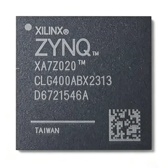
The AMD XC7Z020-2CLG484I is a Zynq-7000 All Programmable SoC (AP SoC) integrating a dual-core ARM Cortex-A9 MPCore processor with an Artix-7 class FPGA fabric in a single 484-ball CSPBGA (19x19 mm) package. The processor subsystem runs at up to 766 MHz with CoreSight debug, while the programmable logic provides 85,000 logic cells, 53,200 LUTs, 106,400 flip-flops, 220 DSP slices, and 4.9 Mb of block RAM. A System on Chip (SoC) is an integrated circuit that consolidates processor, memory controllers, peripherals, and programmable hardware on a single substrate. The Zynq-7000 family pairs an ARM-based processing system (PS) with programmable logic (PL) over high-bandwidth AXI interfaces, reducing board space, power, and system complexity versus discrete processor-plus-FPGA solutions. Key features include a DDR3/DDR3L memory controller with ECC, USB 2.0, Gigabit Ethernet, and support for I/O voltages of 1.2V, 1.5V, 1.8V, 2.5V, and 3.3V. The -2 speed grade supports up to 766 MHz PS operation and 200 MHz+ fabric clocking. The industrial temperature grade (-40C to +100C) targets harsh environments. Architecturally, the PS and PL are independent power domains with defined sequencing requirements (VCCINT, VCCAUX, VCCBRAM, VCCO). The device supports partial reconfiguration, allowing dynamic PL updates while the PS continues running. The memory controller delivers robust DDR3/DDR3L with ECC for industrial and automotive-class designs. Typical applications include motor control, industrial automation, software-defined radio, video processing, and embedded vision. The device suits real-time processing with hardware acceleration, such as machine vision and high-speed data acquisition. Design consideration: ensure correct power-rail sequencing and provide a configuration source (QSPI flash) and PS clock; refer to the Zynq-7000 TRM (UG585) for detailed guidance. Pricing from $60.07 (LCSC, as of 2026-08-29).

USD $49.00 اتصل بنا
XC8664FRIBEKXUMA1 - 8-bit XC800 MCU, 16KB Flash, 38-TSSOP | Infineon
XC8664FRIBEKXUMA1

XC8664FRIBEKXUMA1 - 8-bit XC800 MCU, 16KB Flash, 38-TSSOP | Infineon

The Infineon XC8664FRIBEKXUMA1 is an 8-bit microcontroller built around the XC800 family 8051-compatible CISC core, integrating 16 KB of on-chip Flash memory, 16 KB (16K x 8) program Flash, and 38-pin TSSOP packaging. It operates from a wide supply range of 2.5 V / 3.3 V / 5 V and runs the 8051 core up to 86 MHz (with peripheral domain scaling at 26.67 MHz per the Hotenda listing). According to the manufacturer datasheet, this IC is the first product of a new and advanced 8-bit uC family (XC8oo family), combining a high-performance 8051 core with on-chip Flash memory and powerful on-chip peripherals. An 8-bit microcontroller (MCU) is a single-chip computer that integrates a CPU, RAM, non-volatile program memory, and peripherals such as timers, ADC, and communication interfaces. The 8051 CISC architecture, originally introduced by Intel in 1980, remains one of the most widely deployed embedded cores worldwide and underpins the hypernym hierarchy 8051 -> 8-bit MCU -> microcontroller -> embedded processor -> semiconductor. The XC8664FRIBEKXUMA1 belongs to Infineon's XC866 sub-family, which is targeted at cost-sensitive industrial and automotive body applications requiring deterministic 8-bit performance. Key differentiating features include a TSSOP-38 footprint with gull-wing leads, automotive temperature grade, integrated 16 KB Flash that supports in-application programming, an on-chip ADC and Capture/Compare Unit (CCU6), and a MultiCAN node for automotive networking. The 86 MHz core clock enables high-throughput bit-manipulation routines typical of motor-control and sensor-interface code, while the wide 2.5 V to 5 V supply range simplifies integration into 3.3 V and 5 V mixed-rail systems without external level shifters. The architecture pairs the standard 8051 instruction set with an XC800-specific peripheral set, including the MultiCAN module, the CCU6 motor-control timer, and a 10-bit ADC with up to eight channels. The wide operating voltage window (2.5 V to 5 V) is a defining trait of the XC8oo family and removes the need for separate voltage regulators in many 3.3 V or 5 V designs. Internal PLL, oscillator, and brown-out circuitry further reduce the external BOM. Typical applications include automotive body electronics, sensor interface modules, low-end motor control, and industrial control. The on-chip MultiCAN node makes the part particularly attractive for in-cabin nodes communicating over a CAN bus at 100 kbit/s to 1 Mbit/s. Designers should note that this part is in the older XC8xx family; current Infineon 8-bit roadmaps have shifted to the XC2000 and AURIX families, so lifecycle planning is recommended before committing to long-life designs.

طلب عرض سعر اتصل بنا
XMC1301Q040F0008ABXUMA1 - 32MHz Cortex-M0 MCU, 8KB Flash | Infineon
XMC1301Q040F0008ABXUMA1

XMC1301Q040F0008ABXUMA1 - 32MHz Cortex-M0 MCU, 8KB Flash | Infineon

The Infineon XMC1301Q040F0008ABXUMA1 is a 32-bit ARM Cortex-M0 industrial microcontroller from the XMC1000 family, clocked at 32 MHz with 8 KB of Flash and 16 KB of SRAM, housed in a PG-VQFN-40-13 package (40-pin VQFN, 5x5 mm) with an exposed pad. It integrates the MATH co-processor (CCU6, two Capture/Compare Units) targeted at digital power conversion and industrial motor control, while retaining the ARM Cortex-M0 instruction set for software portability across the XMC family. An ARM Cortex-M0 microcontroller (MCU) is a 32-bit microprocessor core built around the von Neumann architecture with a Thumb-2 instruction set subset, optimized for minimal silicon area and ultra-low active power consumption. The XMC1000 family sits in Infineon's industrial MCU hierarchy: Cortex-M0 (XMC1000) -> Cortex-M3 (XMC4000) -> Cortex-M4F (XMC4500) -> 32-bit industrial microcontrollers, typically used where 8-bit legacy designs cannot deliver the required computational throughput, deterministic timing, or peripheral integration for power-electronic feedback loops. Key features include the CCU6 peripheral for PWM generation with dead-time insertion and emergency stop, a 12-bit A/D converter with up to 12 channels for current/voltage sensing, MATH coprocessor hardware divide, peripheral clock support up to 64 MHz, and a supply voltage range of 1.8 V to 5.5 V. The 32 MHz CPU frequency combined with the deterministic CCU6 timer cluster makes this device well-suited to the digital control loop bandwidth demanded by 100 kHz-class switch-mode power supplies (SMPS) and low-power field-oriented motor control. The architecture is a single-core Cortex-M0 with on-chip Flash, single-cycle multiplier (32-bit result), an AHB-APB peripheral bridge, and Infineon-specific peripherals including the HRPWM (high-resolution PWM) module and a hardware CRC engine. The MATH coprocessor accelerates 32-bit divide and saturation arithmetic for SMPS compensation networks and Clarke/Park transforms on small BLDC motors. Typical applications include digital power supply PFC and PFC+LLC controllers, low-end BLDC/PMSM sensorless fan pumps, LED lighting drivers, and consumer/industrial sensor conditioning. The wide operating voltage range and on-chip peripherals make it popular in 24V industrial sensor hubs and appliance sub-modules that previously relied on discrete 8-bit microcontrollers. When designing with the XMC1301Q040, ensure the exposed thermal pad is soldered to a ground copper pour of at least 50 mm² to meet the theta_JA specified in the datasheet. The CCU6 dead-time register must be loaded before enabling the PWM outputs to avoid shoot-through on a half-bridge. This page synthesizes distributor pricing from DigiKey/Mouser/LCSC, XAIPART partner dropshipping stock levels, and practical design notes that complement the manufacturer's 78-page datasheet with curated cross-references and lifecycle guidance.

طلب عرض سعر اتصل بنا
XMC1302T038X0200A - 32MHz Cortex-M0 MCU | Infineon
XMC1302T038X0200A

XMC1302T038X0200A - 32MHz Cortex-M0 MCU | Infineon

Infineon Technologies XMC1302T038X0200A is a 32-bit ARM Cortex-M0 industrial microcontroller operating at 32 MHz, with 200 KB of flash memory, 16 KB of SRAM, and a 34-I/O PG-TSSOP-38-9 package. It is designed for embedded control, industrial automation, and connected sensor applications requiring deterministic peripheral operation and compact surface-mount integration. What is an ARM Cortex-M0 microcontroller? A microcontroller is a semiconductor device that combines a processor core, memory, analog interfaces, timers, communication peripherals, and digital I/O in one integrated circuit. The ARM Cortex-M0 is a compact 32-bit processor core intended for cost-sensitive embedded systems. The XMC1302 family belongs to the industrial microcontroller hierarchy: MCU, embedded processor, semiconductor, and electronic component. The verified product data identifies an ARM Cortex-M0 core, 32-bit architecture, 32 MHz operating frequency, 200 KB flash, 16 KB SRAM, and a 34-I/O package. The associated Infineon family page describes the device as an industrial MCU with a TSSOP-38 package. These resources make it suitable for motor and machine control, sensor conditioning, digital I/O expansion, communications interfaces, and compact embedded platforms. The 200 KB flash memory supports firmware storage, while the 16 KB SRAM supports working memory for control logic, data acquisition, and peripheral buffering. The 32 MHz operating speed provides a defined computational basis for real-time control loops. The industrial positioning also indicates that the component is intended for embedded applications rather than general-purpose computing. Typical use cases include PLC peripheral modules, industrial sensor nodes, motor-control supervisory logic, building automation controllers, and industrial communication bridges. The compact PG-TSSOP-38-9 package supports surface-mount assembly but requires careful PCB layout and thermal verification for the final operating environment. The supplied distributor and manufacturer results do not provide verified pricing, pin-level details, temperature limits, or complete electrical timing tables, so those values must be confirmed against the manufacturer datasheet before release to production. This page combines the verified Infineon family specifications with practical sourcing, design, and replacement guidance. The provided data does not establish a pin-compatible substitute, current price, lead time, stock status, or complete pinout; engineers should validate those items directly with Infineon or an authorized distributor.

طلب عرض سعر اتصل بنا
XMC1404-F064X0128 - 48MHz ARM Cortex-M0 MCU 128KB Flash LQFP-64
XMC1404-F064X0128

XMC1404-F064X0128 - 48MHz ARM Cortex-M0 MCU 128KB Flash LQFP-64

The Infineon XMC1404-F064X0128 AA is an industrial-grade 32-bit ARM Cortex-M0 microcontroller from the XMC1000 family, delivering up to 48 MHz core performance with 128 KB of embedded flash memory in a PG-LQFP-64-6 package. The device integrates a Cortex-M0 core optimized for low-cost embedded control, 16 KB SRAM, and a rich peripheral set including CCU4/CCU8 PWM timers, POSIF for motor control, multiple USIC channels for UART/SPI/I2C, and a 12-bit ADC. A microcontroller (MCU) is a single-chip computer that integrates a CPU core, program and data memory, and programmable peripherals. The Cortex-M0 is the smallest ARM core, designed for deterministic real-time control in cost-sensitive applications where 8/16-bit MCUs previously dominated. The XMC1400 sits within the XMC1000 family, an industry-targeted extension of Cortex-M0 with hardware PWM and event-request units tailored for power and motion control. Key differentiating features include the CCU8 high-resolution PWM timer (150 ps resolution), HRPWMs for digital power conversion, a 12-bit 1 Msps ADC with up to 12 channels, and Infineon's ERU (Event Request Unit) for hardware event routing without CPU intervention. The device operates from 1.8 V to 5.5 V supply with 5 V-tolerant I/O on most pins, making it suitable for industrial 24 V bus-derived rails after regulation. The architecture combines Cortex-M0 simplicity with motor-control-specific peripherals, achieving deterministic interrupt latency below 25 ns. Integrated POSIF (Position Interface) supports encoder/multi-channel hall-sensor decoding directly in hardware, offloading CPU overhead in FOC motor loops. The XMC1404 family is also AEC-Q100 qualified variants available for automotive motor and lighting. Typical applications include BLDC/PMSM motor control, power conversion (PFC, LLC, solar micro-inverters), LED lighting drivers, industrial HMI panels, and low-cost sensor conditioning. The wide operating temperature range of -40 C to +125 C supports harsh industrial environments. When designing with this MCU, allocate at least 6 layer PCB stack-up for high-frequency signals, use low-ESR ceramic decoupling near each VDD pin, and leverage Infineon DAVE toolchain for code generation. Avoid routing PWM signals near ADC analog inputs to minimize switching noise coupling. This page synthesizes distributor inventory data, drop-in alternatives from the same XMC1400 family, and practical design notes beyond the manufacturer datasheet content.

طلب عرض سعر اتصل بنا
XMC1404Q064X0200AAXUMA1 - 200KB Flash 48MHz Cortex-M0 MCU | Infineon
XMC1404Q064X0200AAXUMA1

XMC1404Q064X0200AAXUMA1 - 200KB Flash 48MHz Cortex-M0 MCU | Infineon

The Infineon XMC1404Q064X0200AAXUMA1 is an industrial-grade 32-bit microcontroller built around an ARM Cortex-M0 core running at 48 MHz, integrating 200 KB of Flash and 16 KB of SRAM, and housed in a PG-VQFN-64-6 package with exposed pad. The XMC1400 family is designed for low-cost embedded control with deterministic peripherals aimed at motor control, power conversion, LED lighting and human-machine interface (HMI) applications. The 'Q064' suffix indicates the 64-pin VQFN package option, '0200' indicates 200 KB Flash, and 'XUMA1' is the tape-and-reel ordering code. A 32-bit microcontroller (MCU) is an integrated circuit that combines a CPU, memory, and programmable peripherals on a single die. The Cortex-M0 is ARM's smallest and most cost-optimized 32-bit core, offering Thumb-2 instruction set compatibility with deterministic interrupt latency. The XMC1000 family sits below the XMC4000 (Cortex-M4F) family in Infineon's portfolio, targeting cost-sensitive real-time control where the M0's instruction efficiency outperforms legacy 8-bit/16-bit architectures. Key features of the XMC1404 include the MATH coprocessor for hardware CORDIC and divide operations, the CCU (Capture Compare Unit 4) timers with hardware PWM support, the POSIF (Position Interface) for encoder feedback, a 12-bit ADC with up to 12 Msps, and the BCCU (Brightness and Colour Control Unit) for LED lighting. The device supports operating voltages from 3.0 V to 5.5 V and ambient temperatures from -40 C to +125 C, making it suitable for industrial environments. The XMC1404 integrates Infineon's proprietary peripheral set on a 130 nm process. The MATH coprocessor offloads trigonometric and arithmetic operations from the core, enabling faster field-oriented control (FOC) loops for motor control. Deterministic interrupt response (typical 12 cycles) and tightly-coupled peripherals minimize jitter in closed-loop applications. The 200 KB Flash supports both in-application programming and read-while-write operation for firmware updates. Typical applications include BLDC/PMSM motor control (PFC plus FOC), industrial automation drives, digital switched-mode power supplies, LED lighting controllers with dimming, and HMI panels with touch or LED feedback. The peripheral combination makes XMC1404 particularly effective for cost-sensitive real-time control loops up to a few kHz. When designing with this MCU, allocate the VQFN-64 thermal pad to a continuous ground copper pour for thermal and electrical performance. Place the 12 MHz crystal or external clock as close as possible to the XTAL pins to minimize EMI susceptibility, and follow Infineon's DAVE SDK for firmware development and code generation. This page consolidates distributor pricing, drop-in same-package alternatives from the XMC1400/XMC1300 family, and practical design notes beyond the manufacturer datasheet to support BOM decisions.

طلب عرض سعر اتصل بنا