The Intel EP20K200EFC484-1X is a 200,000-system-gate FPGA from the APEX 20KE family, integrating 8,320 logic elements, 832 logic array blocks (LABs), 106,496 bits of embedded dual-port RAM, and up to 376 user I/O pins in a 484-ball FineLine BGA (23 × 23 mm, 1.0 mm pitch). It runs from a 1.71–1.89 V core supply (1.8 V nominal), delivers approximately 2.5 ns propagation delay at the -1 speed grade, and is rated for the commercial 0 °C to +85 °C range. The device is programmed through legacy Altera Quartus II (versions 4.x through 13.0sp1). On the XAIPART marketplace, the EP20K200EFC484-1X is listed in stock with 99,999 units available, MOQ 1, with pricing from $285 at qty 1 down to $165 at qty 250 as of 2026-09-12.
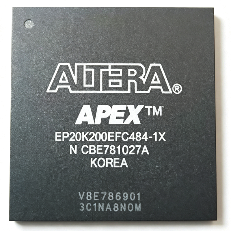
What Exactly Is the EP20K200EFC484-1X and Why Do Engineers Still Specify It?
The EP20K200EFC484-1X belongs to Intel's (formerly Altera) APEX 20KE family, built on a 0.22 µm CMOS process. Its MultiCore architecture combines look-up-table (LUT) logic with embedded dual-port RAM and dedicated carry chains, enabling System-On-A-Programmable-Chip (SOPC) integration. The 'E' suffix marks the enhanced variant over the original APEX 20K, adding on-chip PLLs, LVDS I/O support, and a speed-grade improvement.
Decoding the full part number: 'EP20K200E' = APEX 20KE family at 200K gates, 'F' = FBGA package, 'C' = commercial temperature, '484' = 484 balls, '-1X' = -1 speed grade with lead-free finish. Engineers continue to specify this part for long-life-cycle programs in industrial, aerospace, and defense, where the APEX 20K bitstream is frozen and certification re-spins are costly. Bitstream portability across APEX 20K generations allows DO-254 certification evidence to be reused across hardware revisions on long-life defense programs, dramatically reducing re-qualification cost.
| Parameter | Verified Value |
|---|---|
| Manufacturer | Intel |
| Family | APEX 20KE |
| Maximum System Gates | 200,000 |
| Logic Elements | 8,320 |
| Logic Array Blocks | 832 |
| Total RAM Bits | 106,496 |
| Maximum User I/O | 376 |
| Core Supply (VCCINT) | 1.71 V to 1.89 V (1.8 V nominal) |
| Propagation Delay | 2.5 ns |
| Process Technology | 0.22 µm CMOS |
| Operating Temperature | 0 °C to +85 °C (Commercial) |
| Package | 484-FBGA, 23 × 23 mm, 1.0 mm pitch |
| Architecture | MultiCore (LUT + embedded dual-port RAM) |
| On-chip PLLs | Yes (APEX 20KE enhancement) |
| Mounting Type | Surface Mount |
How Do You Design In the EP20K200EFC484-1X Correctly?
Designing with this FPGA requires attention to its multi-rail power architecture. The device requires separate supplies: VCCINT for the 1.8 V nominal core, VCCIO bank supplies per I/O bank, VCC_PLL for the on-chip phase-locked loops, and VREF reference voltages. Use a sequenced power supply to avoid CMOS latch-up at power-up — this is mandatory, not optional.
Power and I/O Bank Planning
I/O banks can be configured independently for LVTTL, LVCMOS, PCI, and LVDS signalling at 1.8 V, 2.5 V, or 3.3 V depending on VCCIO selection. This bank-level flexibility is one of the chief reasons the part replaced earlier APEX 20K designs: a single die can bridge 3.3 V framers and legacy parallel buses on the same package. Use IBIS models for signal-integrity simulation because the 1.8 V core and LVTTL/LVCMOS I/O standards have very different switching characteristics.
PCB Layout for the 484-FBGA Package
The 484-FBGA FineLine BGA uses a 1.0 mm ball pitch on a 23 × 23 mm body. Use 0.8–1.0 mm PCB pad diameter and a low-CTE substrate for reliable solder joints. For high-vibration environments such as industrial backplanes and avionics LRUs, assemble with corner staking and polymer underfill.
Configuration and Toolchain
The device is programmed using Altera Quartus II design software, legacy versions 4.x through 13.0sp1, with the APEX 20KE device library installed. The Quartus II Programmer generates a .sof or .pof bitstream and drives a MasterBlaster, ByteBlasterMV, or USB-Blaster download cable to the JTAG or passive-serial configuration port. Newer Quartus Prime releases drop APEX 20K support, so archive your legacy Quartus II installation. Quartus II provides timing-driven place-and-route with back-annotation support, and the JTAG port allows in-system bitstream updates in minutes.
Where Is the EP20K200EFC484-1X Used in Real Systems?
Verified application data highlights six deployment scenarios:
Telecommunications line-card glue logic. The 200K gates, 106 Kbits of embedded dual-port RAM, and 376 user I/O pins let one 484-FBGA replace several discrete FIFOs and bus-transceiver CPLDs, bridging legacy parallel buses to TDM/E1 framers. Mixed LVTTL/LVCMOS/PCI I/O banks connect legacy devices alongside 3.3 V framers on the same die.
Custom datapath accelerators. With 832 LABs and dedicated carry chains, the part implements CRC/checksum engines, packet-parsing pipelines, and Reed-Solomon codecs. The -1 speed grade supports 66 MHz PCI and 100 MHz Utopia-style bus interfaces common in infrastructure designs of that era.
Industrial control backplanes. The 376 user I/O pins fan out to dozens of optocoupler-isolated 24 V field devices while LVDS links reach higher-level controllers. On-chip PLLs synchronize multiple clock domains to a single backplane reference.
Legacy ASIC prototyping. The 8,320 logic elements cover medium-complexity SoC glue logic, memory controllers, and PCI bridge functions. JTAG configuration allows in-system bitstream iteration without mask re-spins. For designs exceeding 200K gates, the EP20K400CB652C7 (400K gates, 652-BGA) offers a denser Quartus II-compatible target.
Defense avionics display controllers. Raster-to-buffer scan conversion, ARINC 429 bus bridging, and MIL-STD-1553 protocol termination on multi-decade airframe programs benefit from APEX 20KE bitstream portability.
Test and measurement front-ends. The 106,496 bits of dual-port RAM serve as deep FIFO storage for captured waveforms, and LVDS-capable I/O banks connect directly to high-speed ADC/DAC front-ends without external buffers.
What Are the Drop-In Alternatives to the EP20K200EFC484-1X?
Verified data identifies same-brand APEX 20KE drop-in options. No truly pin-compatible cross-brand replacement exists: the MultiCore architecture, configuration bitstream format, and 484-FBGA ball map are Altera/Intel IP, so Xilinx Spartan-IIE or Virtex-E substitutes require full HDL re-synthesis and PCB rework.
| Parameter | EP20K200EFC484-1X | EP20K200EFC484-2X | EP20K200EFC484-1 | EP20K200EFC484-1N |
|---|---|---|---|---|
| Family / Die | APEX 20KE, 200K gates | APEX 20KE, 200K gates (same die) | APEX 20KE, 200K gates (identical silicon) | APEX 20KE, 200K gates |
| Speed Grade | -1 | -2 (faster) | -1 | -1 (no speed-grade change) |
| Package / Ball Map | 484-FBGA, 23 × 23 mm | Identical 484-FBGA ball-out | Same 23 × 23 mm FBGA footprint | Same footprint |
| Ball / Assembly Finish | Lead-free (X suffix) | Lead-free (X suffix) | SnPb ball finish | Lead-free (N suffix) |
| Drop-in? | — | Yes, drop-in | Yes, drop-in | Yes, drop-in |
Choosing between them: select the EP20K200EFC484-1X if timing closure was achieved at the -1 speed grade or you must match a frozen bitstream for certification. Choose the EP20K200EFC484-2X for new designs wanting the faster -2 grade for additional timing margin — the PCB footprint does not change. For a like-for-like commercial-temperature drop-in with identical silicon, the EP20K200EFC484-1 or EP20K200EFC484-1N apply. [VERIFY_NEEDED: verified full specification tables for EP20K200EFC484-2X, -1, and -1N variants]
What Is the Market and Supply Situation for the EP20K200EFC484-1X?
Supply data contains a status conflict that buyers must understand. The XAIPART product database records the lifecycle status as active, while the verified FAQ data — citing Altera/Intel APEX 20KE product change notifications and Octopart distributor listings — states the part is obsolete/last-time-buy, no longer in active production, available only through authorized distributors holding legacy inventory, with lead times typically 8–16 weeks because supply comes from authorized-channel carryover stock rather than new wafer runs. [DATA_NEEDED: authoritative lifecycle reconciliation — PCN documentation confirming obsolete vs. active status]
Pricing on XAIPART is tiered: $285 at qty ≥ 1, $245 at qty ≥ 10, $215 at qty ≥ 25, $185 at qty ≥ 100, and $165 at qty ≥ 250, as of 2026-09-12. The verified FAQ notes that 1-piece distributor pricing averaged USD 250–320 from franchised distributors as of 2026-09-07, consistent with legacy last-time-buy market pricing. XAIPART currently shows 99,999 units in stock with MOQ 1 as of 2026-09-12.
For industrial environments, note that the -1X 'C' suffix covers only the commercial 0 °C to +85 °C window; extended-thermal programs must migrate to the EP20K200EFI484-2X industrial variant (-40 °C to +100 °C). [DATA_NEEDED: MSL level]; [DATA_NEEDED: RoHS status beyond the lead-free 'X' suffix indication].
What Should Buyers Watch Next for the EP20K200EFC484-1X?
Anchor your procurement decisions to these verified facts. First, the -1 speed grade delivers ~2.5 ns propagation delay and supports 66 MHz PCI interfaces; if your timing margin is thin, qualify the -2X drop-in now while the identical 484-FBGA ball map makes the swap free at the board level. Second, temperature: the commercial 0 °C to +85 °C rating means industrial or avionics LRUs with extended thermal envelopes need the EFI484-2X variant — plan that migration before cabinet environments change. Third, toolchain risk: Quartus Prime drops APEX 20K support, so archive legacy Quartus II 13.0sp1 or earlier installations and licenses today. Fourth, pricing: XAIPART's volume tier reaches $165 per unit at qty ≥ 250 as of 2026-09-12; given the FAQ-reported obsolescence and 8–16 week lead times, place a safety-stock buy against your certified bitstream to protect against allocation. Fifth, verify assembly finish requirements — the '-X' suffix denotes lead-free assembly, whereas the non-X EP20K200EFC484-1 uses SnPb ball finish, which matters for process compatibility on legacy reflow profiles.
Comments
Be the first to comment.
🔐 Please sign in to post a comment.
Don't have an account? Sign up