The EP3SL340F1517I3 is Intel's high-density Stratix III L Field-Programmable Gate Array (FPGA), delivering 337,500 logic elements (LEs), 18,822,144 bits of embedded memory, 576 DSP blocks, and 976 user I/O pins in a 1517-ball flip-chip BGA (FC-FBGA) package. Fabricated on TSMC's 65 nm CMOS process and powered by a 1.1 V core supply, the device runs at up to 500 MHz and is specified for the industrial temperature range of -40C to +100C. Speed grade 3 and configuration via AS, PS, or JTAG make it a complete solution for high-throughput DSP, telecom baseband, video processing, and ASIC-prototyping workloads. It is currently in stock at XAIPART with 99,999 units available, MOQ of 1, priced from $21,833.50 (single unit) down to $18,900 at 100+ units as of 2026-09-14. Note that the device carries a last_time_buy lifecycle status, so new designs and spares strategies should factor that in. This pillar guide consolidates verified specifications, design-in practices, application scenarios, and pricing intelligence into a single authoritative resource for engineers and procurement teams.
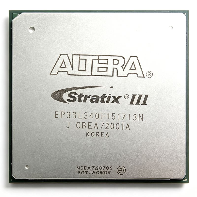
What Is the EP3SL340F1517I3 and Why Do Engineers Choose It?
The EP3SL340F1517I3 belongs to the Stratix III L family, which Intel engineered for the lowest-power, highest-performance tier of the Stratix III generation. An FPGA is a matrix of configurable logic blocks (CLBs), dedicated DSP blocks, embedded memory blocks, and high-speed serial transceivers interconnected by programmable routing fabric — reconfigurable after manufacture for a specific application. The Stratix III family targets high-throughput DSP, packet processing, and ASIC-prototyping workloads specifically.
Three architectural choices distinguish this part. First, the 8-input adaptive logic module (ALM) — the device provides 13,500 ALMs within its 337,500 logic elements — gives synthesis tools finer-grained mapping options than earlier 4-input LUT architectures. Second, 576 dedicated DSP blocks with hardened hardware multipliers raise aggregate DSP throughput into the thousands of GMACS, which is why the family is a mainstay in wideband signal processing. Third, a hardened memory interface supports external DDR3 and QDR II+ memories, with RLDRAM II bridging also supported by the hardened memory controllers.
The I/O system is equally substantial: 976 user I/O pins are distributed across 24 I/O banks and support LVDS, LVTTL, LVCMOS, SSTL, and HSTL standards, both single-ended and differential. Four PLLs handle multi-rate clocking. All of this lives in a 1517-ball FC-FBGA intended for surface-mount assembly.
How Do You Design In the EP3SL340F1517I3 Correctly?
Design-in starts with three board-level and system-level decisions.
1. Power delivery. The 1.1 V core supply rides on a 65 nm process chosen specifically to keep dynamic power lower than the previous Stratix II generation at equivalent throughput. A robust decoupling network on the core rail is required — the datasheet specifies the decoupling network your PCB must incorporate [VERIFY_NEEDED: exact decoupling network component values from Stratix III handbook]. Plan multi-layer power/ground planes given the 1517-ball footprint.
2. Configuration scheme. The device supports AS (Active Serial), PS (Passive Serial), and JTAG configuration per the Stratix III family. JTAG is the standard path for in-system debugging; AS suits production boot from serial flash. Select your configuration device and boot chain early, because the configuration pins share banks with user I/O in some layouts.
3. Toolchain and timing closure. Use the Altera Quartus II toolchain for synthesis, place-and-route, and timing closure. For DSP-heavy designs, Quartus II DSP Builder accelerates model-based design of FIR and FFT cores, and the Quartus II IP catalog includes drop-in memory-interface IP. Quartus II Qsys enables rapid system integration for control and DSP pipelines.
Because the maximum operating frequency is 500 MHz and the speed grade is 3, budget your timing constraints conservatively on the fastest fabric paths and use the hardened memory controllers rather than soft-logic memory interfaces where possible — the hardened interface is one of the family's headline differentiators for DDR3 and QDR II+ connectivity.
Thermal design matters as well: the industrial -40C to +100C operating range gives headroom, but a 337,500-LE device running thousands of GMACS of DSP throughput in a sealed enclosure requires a calculated heatsink and airflow plan [VERIFY_NEEDED: package thermal resistance values from Stratix III handbook].
Where Does the EP3SL340F1517I3 Deliver the Most Value? Six Verified Application Scenarios
High-performance ASIC prototyping. The 337,500 logic elements and 18.8 Mbit of embedded block memory let teams emulate ASIC designs of 20–30 million gates with full RTL visibility before committing to a mask cycle, reducing or eliminating multi-FPGA partitioning. The 976 user I/O pins across 24 banks fan out directly to memory interfaces and external test fixtures.
Telecom baseband processing. 576 DSP blocks, DDR3/QDR II+ external memory support, and 4 PLLs for multi-rate clocking fit baseband card designs; the 1517-FCBGA exposes enough I/O for parallel ADC/DAC interfaces and CPRI/OBSAI links. Compared with Stratix II, the Stratix III L family halves dynamic power at iso-throughput, easing thermal budgets in sealed outdoor base-station cabinets within the -40C to +100C range.
High-end video and image processing. 18.8 Mbit of fast on-chip memory handles line buffering, and 24 I/O banks allow multiple camera/display interfaces to coexist. Real-time 4K processing, multi-channel SDI bridging, and computer-vision pre-processing run directly in fabric for surveillance and medical-imaging enclosures.
Military/aerospace signal intelligence. The industrial temperature range, large logic capacity, and high DSP throughput suit wideband receivers, FFT-based channelizers, and adaptive beam-formers in a single device. The 65 nm Stratix III process is mature for long-lifecycle defense programs, and Altera/Intel has published military-temperature variants (EP3SE/EP3SL extended screening) for higher-grade applications.
High-speed memory interface bridging. Hardened memory controllers plus 4 PLLs support bridging between DDR3, QDR II+, RLDRAM II, and legacy interfaces — enough 976 I/O across 24 banks for multi-port memory bridges on networking line cards and in high-performance compute.
Test and measurement instrumentation. High logic density, 576 DSP blocks for digital down-conversion, and 976 I/O for parallel ADC/DAC interfacing enable arbitrary waveform generators, real-time spectrum analyzers, and protocol analyzers in both bench-top and field-portable instruments.
What Are the Verified Specifications of the EP3SL340F1517I3?
| Parameter | EP3SL340F1517I3 (Verified) |
|---|---|
| Manufacturer | Intel |
| Family | Stratix III L |
| Logic Elements | 337,500 |
| Adaptive Logic Modules (ALMs) | 13,500 |
| Total Memory Bits | 18,822,144 |
| DSP Blocks | 576 |
| User I/O Pins | 976 |
| I/O Banks | 24 |
| PLLs | 4 |
| Core Voltage | 1.1 V |
| Process Technology | 65 nm CMOS |
| Maximum Operating Frequency | 500 MHz |
| Configuration Method | AS / PS / JTAG |
| Package | 1517-BBGA, FCBGA (Flip-Chip) |
| Mounting Type | Surface Mount |
| Temperature Grade / Range | I (Industrial), -40C to +100C |
| Speed Grade | 3 |
Full electrical timing tables, I/O standard support details, and package mechanical drawings are found in the Stratix III handbook, linked on the EP3SL340F1517I3 product page. Detailed pin-level data lives on the product page; no abbreviated pinout is reproduced here.
Which Alternatives Can Replace the EP3SL340F1517I3?
XAIPART's verified database currently lists no cross-verified drop-in alternatives for the EP3SL340F1517I3. Within the Stratix III L family itself, options exist at different densities and speed grades [DATA_NEEDED: same-family alternative MPNs with verified specs]. Until verified alternative data is added, we recommend anchoring comparisons only to the specifications table above and consulting Intel's Stratix III family documentation for density/speed-grade variants of the same package. Substituting a different package or family (e.g., EP3SE variants) changes pinout, I/O count, and timing characteristics and requires re-verification [VERIFY_NEEDED: cross-family substitution feasibility].
When evaluating any substitute, verify against these anchor specs: 337,500 LEs, 13,500 ALMs, 18,822,144 memory bits, 576 DSP blocks, 976 user I/O across 24 banks, 4 PLLs, 1.1 V core, 65 nm process, 500 MHz maximum frequency, speed grade 3, industrial -40C to +100C, and the 1517-ball FC-FBGA package.
How Much Does the EP3SL340F1517I3 Cost and What Is Its Supply Situation?
Verified tiered pricing as of 2026-09-14:
| Quantity | Unit Price (USD) |
|---|---|
| 1+ | $21,833.50 |
| 5+ | $21,500.00 |
| 10+ | $21,050.00 |
| 25+ | $20,100.00 |
| 100+ | $18,900.00 |
That is a 13.4% reduction from single-unit to 100+ unit pricing — meaningful savings for production programs or multi-unit prototyping farms. XAIPART lists 99,999 units in stock with an MOQ of 1, so prototypes and low-volume builds can ship immediately.
The critical procurement signal is lifecycle status: last_time_buy. This means Intel is in the final ordering window for this device. For defense, aerospace, and long-lifecycle industrial programs — the very markets this FPGA serves — a last-time-buy typically triggers lifetime-buy planning. Teams should calculate total program consumption (production units plus spares and RMA reserve) and place a single consolidated order while stock remains. With 99,999 units listed as of 2026-09-14, near-term availability is strong, but last_time_buy status means that stock will not be replenished [VERIFY_NEEDED: official Intel discontinuation/last-order date for the Stratix III family]. Browse related devices on the FPGA & CPLD category page.
What Should Buyers and Engineers Watch Next for Stratix III-Class FPGAs?
Three trends anchor directly to the verified specs of this device.
Lifecycle migration planning. With last_time_buy status confirmed, new designs should not start on this part unless the program horizon is short or a lifetime buy is budgeted. The mature 65 nm process remains an advantage for defense programs needing proven silicon, but roadmap continuity now depends on successor families [DATA_NEEDED: Intel-recommended successor device for Stratix III designs].
Price-tier leverage before the window closes. The verified price ladder — $21,833.50 at qty 1 down to $18,900 at qty 100+ as of 2026-09-14 — rewards consolidated ordering. A team needing 30 units over two years saves $51,005 total by ordering 30 at once ($20,100 each) versus three batches of 10 ($21,050 each).
Power and density trade-offs stay favorable. The 1.1 V core on 65 nm halving dynamic power versus Stratix II at iso-throughput means existing Stratix III sockets remain thermally competitive; any migration must match that power profile as well as the 337,500-LE and 576-DSP-block capacity. Designs exploiting the 976 user I/O, 24 I/O banks, and hardened DDR3/QDR II+ interfaces should treat pin-compatible replacement as mandatory, not optional.
For engineers maintaining existing sockets, the practical checklist is: lock your Quartus II project and toolchain version, document your configuration scheme (AS/PS/JTAG), freeze the decoupling and memory-interface reference designs, and place your lifetime buy. Order the EP3SL340F1517I3 on XAIPART while the last_time_buy window and stock remain open.
Comments
Be the first to comment.
🔐 Please sign in to post a comment.
Don't have an account? Sign up