The Intel EP4CE40F23C7N is a Cyclone IV E Field Programmable Gate Array (FPGA) built on a 60 nm low-power CMOS process, delivering 39,600 logic elements, 1,161,216 bits of embedded M9K memory, and 116 embedded 18×18 hardware multipliers in a 484-ball FineLine BGA package with a 1.0 mm ball pitch. The device exposes up to 328 user I/O pins, integrates 4 PLLs for clock management, and supports DDR, DDR2 SDRAM, and QDRII SRAM external memory interfaces. Configuration is handled through JTAG, Active Serial (AS), or Passive Serial (PS) modes, and the commercial temperature grade covers 0°C to +85°C with RoHS compliance. As of 2026-09-12, the EP4CE40F23C7N is an active-lifecycle part in stock at XAIPART with 99,999 units available, MOQ of 1, and tiered pricing from $35.72 at qty 1 down to $21.80 at qty 1000.
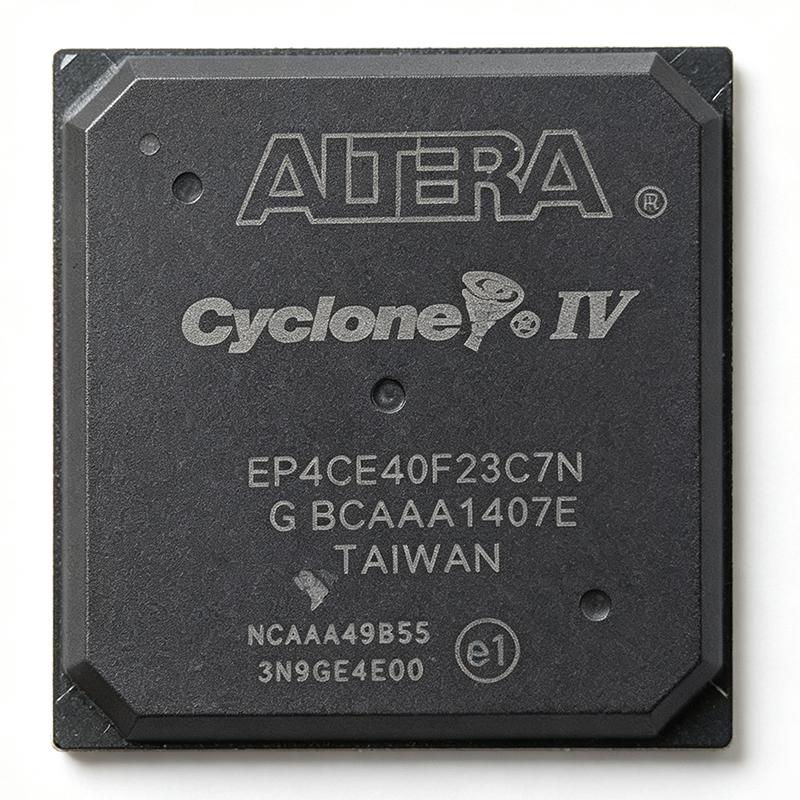
What Should Engineers Know Before Buying the EP4CE40F23C7N?
Before committing the EP4CE40F23C7N to a design, buyers should anchor their decision on the verified specifications below. These values come directly from the XAIPART product database and align with the Intel Cyclone IV Device Handbook.
| Parameter | EP4CE40F23C7N |
|---|---|
| Manufacturer | Intel (formerly Altera) |
| Product Family | Cyclone IV E |
| Logic Elements | 39,600 |
| Embedded Memory | 1,161,216 bits (~113.4 Kbytes, M9K blocks) |
| Embedded 18×18 Multipliers | 116 |
| Maximum User I/O | 328 |
| PLLs | 4 |
| Distributed RAM | 66.5 Kbits |
| Process Technology | 60 nm low-power CMOS |
| Core Voltage | 1.2 V (typical) |
| Package | 484-ball FineLine BGA (FBGA), 1.0 mm ball pitch |
| Operating Temperature | 0°C to +85°C (commercial) |
| Speed Grade | C7 |
| Configuration Methods | JTAG, Active Serial (AS), Passive Serial (PS) |
| RoHS Status | Compliant |
Availability is strong on XAIPART: 99,999 units in stock, MOQ of 1, and volume pricing of $21.80 per unit at qty 1000 as of 2026-09-12. The part remains in active production under Intel's Product Lifecycle program, with no announced end-of-life for the EP4CE40 variant as of 2026-09-10.
How Do You Select and Design In the EP4CE40F23C7N?
Design-in success with the EP4CE40F23C7N starts with matching the device's resources to your workload, then follows Intel's recommended board-level practices.
Step 1: Match Logic, Memory, and DSP Resources
The 39,600 logic elements place this device in the mid-density range of the Cyclone IV E family, suitable for medium-complexity logic, DSP, and bridging designs that do not require the larger EP4CE55 or EP4CE75 variants. Budget your design against three resource pools: 39,600 LEs for control and datapath logic, 1,161,216 bits of M9K block RAM for line buffers, packet FIFOs, and coefficient storage, and 116 embedded 18×18 multipliers for FIR filters, FFT engines, and control-loop math. The 66.5 Kbits of distributed RAM handle shallow, wide FIFOs and register files that would waste block RAM.
Step 2: Plan the Clock Architecture
The four general-purpose PLLs synthesize independent clock domains. In a typical video or SDR design, one PLL generates the capture clock, another the processing clock, and a third the output or interface clock. Because the PLLs are hard IP, they deliver low-jitter clocks without consuming logic elements.
Step 3: Use the Right Configuration Scheme
For production, Active Serial (AS) configuration from a serial flash keeps the BOM minimal and allows field updates. JTAG remains the fastest path for board bring-up and in-system debugging; reserve Passive Serial for designs where an external controller manages configuration.
Step 4: Power and Decoupling
The core runs at a typical 1.2 V. Decouple each power pin with 100 nF and 10 µF capacitors placed near the ball, and follow Intel's recommended PCB layout guidelines for the FBGA package. The 1.0 mm ball pitch of the 484-FBGA is compatible with standard multilayer PCB stackups and conventional BGA assembly processes.
Step 5: Toolchain
Use the Intel Quartus II design software for synthesis, place-and-route, timing analysis, and bitstream generation. Quartus II v13.1 is the latest version with full Cyclone IV E support; after that release, the family transitioned to legacy support in Quartus Prime. Plan your toolchain installation accordingly, since new team members will need access to the legacy release.
Step 6: Timing Closure on the C7 Speed Grade
The C7 speed grade is the slowest commercial grade in the family, so designs running near the top of the achievable Fmax should constrain timing early and verify closure in Quartus before finalizing the PCB. If timing margin is tight, the pin-compatible EP4CE40F23C6N (faster C6 grade) is a drop-in PCB option.
What Are the Drop-In Alternatives to the EP4CE40F23C7N?
Within the Cyclone IV E family, four verified sibling parts share the same die and 484-FBGA footprint and can be swapped on the same PCB. The comparison below uses data verified in the XAIPART product FAQ records.
| Parameter | EP4CE40F23C7N | EP4CE40F23C8N | EP4CE40F23C6N | EP4CE40F23I7N | EP4CE40F23A7N |
|---|---|---|---|---|---|
| Speed Grade | C7 | C8 (slower) | C6 (faster) | I7 | A7 (automotive) |
| Temperature Range | 0°C to +85°C (commercial) | Commercial | Commercial | -40°C to +100°C (industrial) | -40°C to +125°C (automotive) |
| Package / Footprint | 484-FBGA | 484-FBGA (pin-compatible) | 484-FBGA (pin-compatible) | 484-FBGA (same footprint) | 484-FBGA (same package) |
| Best Use | General commercial designs | Best drop-in replacement; cost-optimized | Tighter timing margin | Harsh environments | Automotive temperature |
Selection guidance: substituting the industrial EP4CE40F23I7N or automotive EP4CE40F23A7N for the commercial EP4CE40F23C7N is electrically safe on the same footprint, but adds cost with no benefit in a standard enclosure. The EP4CE40F23C8N is the best drop-in replacement when the C7 is unavailable, since the only difference is a slightly slower timing closure target that most designs never notice. Against the Xilinx (now AMD) XC7A35T-1CPG236C referenced in buyer comparisons, the EP4CE40F23C7N offers more logic (39.6K LE vs ~33K LC) and far more user I/O (328 vs ~106), while the 28 nm Artix-7 adds transceivers in a smaller 236-ball BGA; for high-I/O industrial control, the EP4CE40 is the better fit. [VERIFY_NEEDED: XC7A35T pricing and stock data not provided in this dataset]
Where Does the EP4CE40F23C7N Fit in the Market and Supply Chain?
The EP4CE40F23C7N holds active lifecycle status and remains in production under Intel's Product Lifecycle program, with no announced end-of-life as of 2026-09-10. Cyclone IV E devices have moved to long-term product status, which signals Intel's commitment to continued supply for existing designs rather than new-design promotion.
From a supply perspective, lead time runs 8 to 12 weeks from Intel's authorized distributors due to the legacy 60 nm process node. DigiKey and Mouser typically maintain some stock for small quantities, but production volumes require placing orders well in advance of the build cycle. XAIPART currently lists 99,999 units in stock with MOQ of 1, and entry pricing at $35.72 (qty 1) as of 2026-09-12, dropping to $28.40 at qty 100 and $21.80 at qty 1000. [DATA_NEEDED: industry market-share statistics for the Cyclone IV E family]
What Trends Should Buyers Watch for the EP4CE40F23C7N?
Three trends matter for procurement and engineering teams anchoring designs to this part:
1. Legacy-node supply planning. The 8-to-12-week lead time tied to the 60 nm process means production buyers should carry buffer inventory or secure volume agreements; the verified stock of 99,999 units on XAIPART as of 2026-09-12 provides near-term coverage for prototyping and pilot builds.
2. Speed-grade flexibility as a hedge. Because the C8, C6, I7, and A7 siblings are pin-to-pin compatible on the same 484-FBGA footprint, qualify your PCB for the full EP4CE40F23 family. This lets purchasing switch grades to manage cost or timing margin without a respin.
3. Toolchain lifecycle awareness. Full Cyclone IV E support ends at Quartus II v13.1, with the family in legacy support under Quartus Prime. Freeze and archive your toolchain version per project so builds remain reproducible for the life of the product.
For new designs targeting high-I/O industrial control, video acquisition, or protocol bridging, the EP4CE40F23C7N's combination of 328 user I/Os, 116 multipliers, and 1.16 Mbits of embedded memory still delivers consolidated single-chip control that reduces PCB area and BOM cost versus DSP+MCU pairs. Check the EP4CE40F23C7N product page on XAIPART for live pricing, and browse the FPGA & CPLD category and XAIPART engineering blog for related design guides.
Comments
Be the first to comment.
🔐 Please sign in to post a comment.
Don't have an account? Sign up