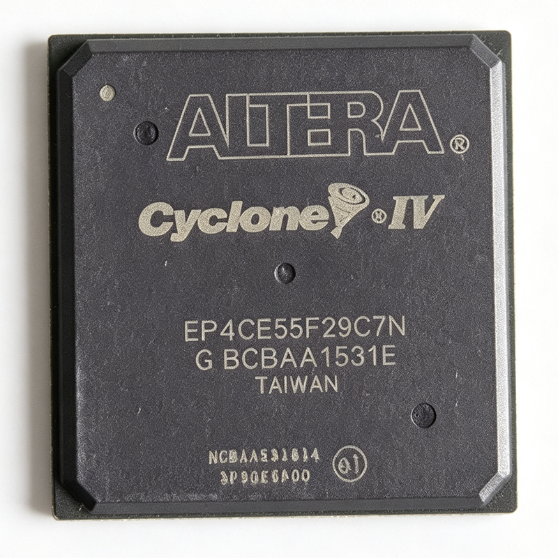
The Intel (formerly Altera) EP4CE55F29C7N is a Cyclone IV E family FPGA delivering 55,856 logic elements, 3,491 configurable logic blocks (CLBs), 2,396,160 bits of embedded SRAM, and 374 user I/Os in a 780-ball FineLine BGA (F29) package measuring 29 mm x 29 mm with a 1.0 mm ball pitch. It runs from a 1.2 V core supply, carries the -7 (C7) speed grade, and is rated for the 0C to +85C commercial temperature range with RoHS-compliant, lead-free construction. The part is active, in stock on XAIPART (99,999 units, MOQ 1), and priced from $215 at qty 1 down to $138 at qty 1,000 as of 2026-09-12. It suits industrial motor control, video processing, ADAS pre-processing, communications bridging, test instrumentation, and consumer display designs that need 50K+ LEs and 300+ I/Os without moving to EP4CE75 or EP4CE115 tiers.
What Are the Quick Answers Every EP4CE55F29C7N Buyer Needs First?
Engineers sourcing this FPGA most often ask about logic capacity, package mechanics, configuration options, and price. The verified facts: the device belongs to the Cyclone IV E family, offers 55,856 LEs and 3,491 CLBs, and provides 2,396,160 embedded RAM bits (M9K blocks). The F29 suffix encodes the 780-ball FBGA package at 1.0 mm pitch — fine-pitch microvia PCB technology is required. Configuration supports JTAG, Active Serial, and Passive Parallel modes with built-in decompression and encryption for IP protection. The device supports Nios II soft cores and multiple I/O standards including LVDS, LVTTL, LVCMOS, SSTL, and HSTL. Full FAQ answers appear in the structured FAQ block on this page; XAIPART lists real-time stock and tiered pricing on the EP4CE55F29C7N product page.
How Do You Select and Design In the EP4CE55F29C7N Correctly?
Step 1 — Confirm density fit. Choose the EP4CE55F29C7N when your design needs more than approximately 40,000 logic elements, more than 200 user I/Os, or more than 1 Mbit of internal memory beyond the EP4CE40F29C7N. At 55,856 LEs, it is the right tier when smaller Cyclone IV E devices run out of fabric but the EP4CE75 or EP4CE115 would be over-provisioned.
Step 2 — Verify speed grade timing margin. The -7 (C7) grade is the mid-performance tier of the family, balancing timing margin against cost. If internal-path timing closure is tight, the pin-compatible EP4CE55F29C8N offers approximately 15 percent faster internal timing per Intel's speed-grade characterization data — no PCB redesign required.
Step 3 — Plan the power architecture. The core runs at a nominal 1.2 V. Because core and I/O supply currents vary significantly with logic utilization and toggle rates, run the Intel Quartus Prime Early Power Estimator before finalizing pin assignment and regulator sizing. The I/O banks support multiple standards (LVDS, LVTTL, LVCMOS, SSTL, HSTL), enabling direct interfacing with 1.8 V image sensors and 3.3 V display drivers in the same design [VERIFY_NEEDED: exact per-bank I/O voltage ranges].
Step 4 — Design the PCB for 1.0 mm-pitch FBGA. The 29 mm x 29 mm, 780-ball package requires microvia stack-up technology, an appropriate escape routing plan, and a disciplined decoupling strategy around the 1.2 V core rail. Surface-mount assembly with lead-free reflow profiles is required given the RoHS lead-free construction.
Step 5 — Choose the configuration chain. The device supports JTAG for development and in-system reprogramming (useful for factory calibration in test equipment), plus Active Serial and Passive Parallel modes for production with a companion configuration device. Built-in decompression reduces configuration storage, and the encryption engine protects design IP [VERIFY_NEEDED: supported encryption key size].
Step 6 — Exploit embedded resources. The 2,396,160 M9K RAM bits support FOC lookup tables, frame buffers, and FIR coefficient storage without external memory. Embedded multipliers suit DSP pipelines. The device hosts Nios II soft cores for housekeeping alongside deterministic hardware accelerators [DATA_NEEDED: 18x18 embedded multiplier count] [DATA_NEEDED: PLL count].
What Are the Best Alternatives and Drop-In Replacements for the EP4CE55F29C7N?
Within the verified data, true drop-in replacements are the speed-grade siblings in the identical 780-FBGA F29 package. Note: XAIPART's database does not currently carry complete specification records for the variants below, so the comparison covers the verified parameters of the base part; variant timing deltas come from Intel's ordering-guide data cited in the FAQ records.
| Parameter | EP4CE55F29C7N | EP4CE55F29C8N | EP4CE55F29C6N |
|---|---|---|---|
| Package | 780-FBGA F29, 29 mm x 29 mm, 1.0 mm pitch | 780-FBGA F29 (same) | 780-FBGA F29 (same) |
| Speed grade | -7 (C7) | -8 (C8) | -6 (C6) |
| Logic Elements | 55,856 | [DATA_NEEDED: LE count] | [DATA_NEEDED: LE count] |
| Relative internal timing | Baseline | ~15% faster than -7 (per Intel speed-grade characterization) | [DATA_NEEDED: timing vs -7] |
| Drop-in compatible? | — | Yes, pin-compatible, no PCB change | Yes, pin-compatible (lower cost, lower performance) |
| Verified price on XAIPART | $215 (qty 1) / $138 (qty 1,000) as of 2026-09-12 | [DATA_NEEDED: pricing] | [DATA_NEEDED: pricing] |
One part to avoid as a replacement: the EP4CE55F23A7N shares the Cyclone IV E family and -7 speed grade but uses the F23 484-FBGA package. It is not drop-in compatible — using it forces a PCB redesign. [VERIFY_NEEDED: pricing and stock for EP4CE55F29C8N and EP4CE55F29C6N on XAIPART]
Where Does the EP4CE55F29C7N Fit in Real-World Applications?
Industrial motor control. The 55,856 LEs and 374 user I/Os integrate PWM generators, encoder interfaces, and current/voltage sensing for multi-axis drives, while the 2,396,160 M9K RAM bits hold field-oriented-control lookup tables without external memory. LVDS and HSTL I/O support high-speed resolver feedback, and Nios II soft cores handle housekeeping.
Video and image processing. Embedded multipliers and M9K blocks implement real-time 2D filtering at 1080p60 pixel rates; the 374 I/Os accept parallel RGB/YCbCr buses and BT.656/BT.1120 streams and drive HDMI, LVDS, or MIPI bridges. Quartus Prime DSP Builder compiles the chain with timing closure at the -7 grade.
Automotive ADAS pre-processing. The device aggregates parallel sensor data and buffers raw frames in the 2.4 Mbit embedded RAM before handoff to an SoC. For under-hood temperatures, designers should use the industrial variant EP4CE55F29I7N, rated -40C to +100C, in the same F29 package. Note the base C7N part is commercial-grade only (0C to +85C).
Communications infrastructure. High I/O count supports parallel TDM interfaces; embedded multipliers handle encryption and FEC at line rate. The PLL resources generate independent clocks for fabric and external PHYs in multi-rate and SDR front-end designs [DATA_NEEDED: PLL count for clock-planning confirmation].
Test and measurement. Logic-analyzer probe heads, protocol exercisers, and AWGs exploit the 374 I/Os, embedded RAM, and 18x18 multipliers for FFT-based analysis; the -7 grade supports 200+ MHz internal fabric clocks with TimeQuest-verified timing. JTAG enables in-system reprogramming during factory calibration.
Consumer and embedded displays. Kiosks, gaming peripherals, and signage controllers use the 2.4 Mbit RAM for frame buffers and gesture lookup tables, with 374 I/Os interfacing touch controllers, RGB/LVDS panels, and audio codecs, and Nios II cores running application-layer logic.
What Is a Worked Design Example Using the EP4CE55F29C7N?
Problem: A multi-axis industrial servo drive needs a central controller integrating six PWM channels, encoder inputs, and FOC coefficient storage without external SRAM, on a cost-controlled bill of materials.
Approach: Use one EP4CE55F29C7N as the central control FPGA. Allocate LEs to six three-phase PWM modulators and encoder-interface logic, place FOC lookup tables and ripple-compensation coefficients in M9K blocks, add a Nios II core for housekeeping and RS-485/CAN gateway logic, and use LVDS I/O for resolver feedback.
Calculations: Budget fabric utilization at 70% → 55,856 LEs x 0.70 ≈ 39,099 LEs available for control logic; memory budget at 2,396,160 bits comfortably holds six axis coefficient sets plus safety logic scratch RAM (exact per-axis coefficients depend on the motor-control algorithm — confirm during Quartus compilation) [VERIFY_NEEDED: per-axis resource utilization figures]. Power: run the Quartus Prime Early Power Estimator with final toggle rates before sizing the 1.2 V core regulator [VERIFY_NEEDED: core current estimate].
Results: A single-FPGA servo controller with no external coefficient memory, timing closure achievable at the -7 speed grade, and unit cost of $215 at qty 1 down to $138 at qty 1,000 as of 2026-09-12 on XAIPART.
Is the EP4CE55F29C7N Active, In Stock, and Safe to Design In for New Programs?
Lifecycle status is active per the XAIPART database. The device is shipping with 99,999 units in stock on XAIPART as of 2026-09-12, MOQ 1, tiered pricing $215 / $195 / $175 / $155 / $138 at qty 1 / 10 / 100 / 500 / 1,000 as of 2026-09-12. Intel's newer Cyclone V and Cyclone 10 families are recommended for brand-new designs, but the Cyclone IV E family remains in production for long-life industrial and automotive programs that require proven, stable silicon. When out of stock at distributors, typical commercial-temperature Cyclone IV E lead time runs 6-12 weeks depending on Intel's factory schedule. [DATA_NEEDED: end-of-life / last-time-buy policy dates for Cyclone IV E]
What Should Buyers Watch Next for the EP4CE55F29C7N?
First, watch pricing tiers: the verified spread is wide — $215 at qty 1 versus $138 at qty 1,000 (as of 2026-09-12) — so consolidating purchases across production batches yields a 36% unit-price reduction at the top verified tier. Second, watch speed grade availability: if timing margin becomes the bottleneck during late-stage closure, the pin-compatible EP4CE55F29C8N upgrades in place with no PCB change. Third, watch temperature grade: any extension of the application toward industrial environments requires the EP4CE55F29I7N variant (-40C to +100C); design the PCB once in the F29 package so either grade drops in. Fourth, watch configuration-device supply since Active Serial and Passive Parallel production modes depend on companion parts. Finally, for net-new programs, evaluate whether Cyclone V or Cyclone 10 better fits the roadmap while recognizing Cyclone IV E remains active and fully supported for existing and long-life designs. Monitor real-time stock on the XAIPART EP4CE55F29C7N page and browse the wider FPGA & CPLD catalog and XAIPART technical guides for adjacent selection advice.
Comments
Be the first to comment.
🔐 Please sign in to post a comment.
Don't have an account? Sign up