The Intel (formerly Altera) EP4CGX30CF19I7N is a Cyclone IV GX field-programmable gate array delivering 29,440 logic elements, 1,105,920 bits of embedded memory, 66 18x18 DSP multipliers, and four integrated 3.125 Gbps full-duplex transceivers in a 324-ball fine-pitch BGA (F19, 19x19 mm, 0.8 mm ball pitch) with up to 150 user I/O. The 'I' suffix guarantees industrial operation from -40C to +100C junction temperature, and the 'N' suffix denotes lead-free, RoHS-compliant terminations. The device is active in Intel's lifecycle status and is in stock at XAIPART with 99,999 units available, MOQ 1, priced from $122.31 at qty 1 down to $76.40 at 1,000 pieces as of 2026-09-12. Its hardened PCIe Gen1 IP, four PLLs, and DDR/DDR2/DDR3 memory controller support make it a proven choice for PCIe endpoint cards, industrial machine vision, motor control, SDR front ends, and protocol bridging.
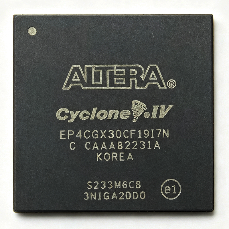
What Is the EP4CGX30CF19I7N and Why Do Engineers Choose It?
The EP4CGX30CF19I7N is the mid-density member of Intel's Cyclone IV GX family, built on a 60 nm low-power process with a 1.2 V typical core supply (1.1 V variant also referenced). It occupies the FPGA tier of the programmable logic hierarchy (PLDs, CPLDs, FPGAs, ICs), giving design teams a re-programmable, parallel-processing alternative to ASICs and microcontrollers for high-throughput, low-latency, or interface-bridging workloads.
What sets this part apart at its price point is the combination of general-purpose fabric and hard serial connectivity. The four full-duplex 3.125 Gbps transceivers natively support PCIe Gen1, Gigabit Ethernet, Serial RapidIO, and CPRI, eliminating external PHY chips in many protocol-bridging designs. A hardened PCIe IP block implements the transaction layer, data link layer, and PHY layer, so a Gen1 x1 endpoint can be instantiated without consuming fabric logic. Meanwhile, 66 18x18 multipliers handle DSP work such as FIR filtering, FFT engines, and image preprocessing, and 720 Kbits of MLAB memory plus hard memory controllers supporting DDR/DDR2/DDR3 SDRAM, QDRII+ SRAM, and RLDRAM II cover buffering needs.
Per the Cyclone IV GX handbook, all resources are simultaneously available with no banking conflicts, so you can plan floorplans without reserving fabric for hidden contention.
What Are the Key Specifications of the EP4CGX30CF19I7N?
| Parameter | Value |
|---|---|
| Manufacturer | Intel (formerly Altera) |
| Series / Family | Cyclone IV GX |
| Logic Elements | 29,440 |
| Embedded Memory | 1,105,920 bits (720 Kbits MLAB) |
| DSP Blocks (18x18 multipliers) | 66 |
| PLLs | 4 |
| Transceivers | 4 full-duplex at 3.125 Gbps (8 channels total) |
| User I/O | 150 |
| Process Technology | 60 nm low-power |
| Core Voltage | 1.2 V typical (1.1 V variant) |
| Package | 324-ball FBGA (F19, 19x19 mm, 0.8 mm pitch) |
| Mounting Type | Surface Mount |
| Operating Temperature | -40C to +100C (TJ, industrial) |
| Speed Grade | 7 |
| RoHS Status | Compliant (N suffix = lead-free balls) |
| Configuration | Serial / parallel flash via Quartus |
How Do You Design In the EP4CGX30CF19I7N? A Practical Technical Guide
Designing with the EP4CGX30CF19I7N follows three stages: toolchain setup, power and I/O planning, and transceiver-aware PCB layout.
1. Toolchain
The device requires Quartus II (legacy) or Quartus Prime (current) software for synthesis, place-and-route, timing analysis, and bitstream generation. Quartus Prime Lite edition supports Cyclone IV GX free of charge, with the ModelSim-Intel FPGA starter edition for simulation. Configuration uses serial or parallel flash via Quartus.
2. Power and I/O Banking
The core runs from a 1.2 V supply (with a 1.1 V variant referenced in the verified data), while the eight I/O banks each use their own VCCIO supply so you can mix voltage domains across the 150 user I/O. The pinout groups IO, VCCIO, and GND balls per bank (for example, A1 = IO bank 1 with A2 = VCCIO1; C1 = IO bank 2; E1 = IO bank 3 with E2 = VCCIO3). Plan bank assignments early so each VCCIO rail matches the signaling standard of its connected peripherals.
3. Transceiver and Clock Layout
The 3.125 Gbps channels demand controlled-impedance differential traces and continuous reference planes. Route transceiver reference clocks cleanly to REFCLK_0 (pin U1) and REFCLK_1 (pin V1), keep the VCCA analog supply (pin U2) isolated and well-decoupled, and maintain solid ground return under every TX/RX differential pair (W1/W2 for channel 0, Y1/Y2 for channel 1). Avoid splitting reference planes beneath high-speed pairs, and keep the F19 package's 0.8 mm ball pitch escape routing short at these edge rates.
4. Memory Interfaces
Hard memory controllers support DDR/DDR2/DDR3 SDRAM, QDRII+ SRAM, and RLDRAM II, offloading PHY timing from fabric. Budget the 1,105,920 embedded memory bits for descriptors and line buffers before committing to external memory; many designs stage data entirely on-chip.
Where Is the EP4CGX30CF19I7N Used? Six Proven Application Scenarios
The verified application data highlights six dominant use cases:
- PCI Express endpoint cards. The hardened PCIe Gen1 x1 endpoint plus 29,440 LEs leaves ample room for DMA engines and register interfaces, while 1,105,920 bits of RAM handle scatter-gather descriptors.
- Industrial machine vision. 66 18x18 multipliers run Bayer-to-RGB demosaicing and preprocessing at line rates up to 80 MHz, bridging Camera Link, CoaXPress, or GigE Vision streams; the F19 package fits PC/104 and COM Express carriers.
- Motor control and factory automation. Four PLLs generate independent switching frequencies for up to four inverter stages with sub-microsecond current-loop sampling; transceivers carry EtherCAT, PROFINET, or SERCOS III.
- Software-defined radio. 66 DSP blocks implement FIR filters and FFT engines, and 1,105,920 bits of block RAM stage 16K-sample FFT windows without external memory.
- Broadcast video processing. Transceivers accept 3G-SDI inputs at 2.97 Gbps per channel while fabric runs scalers and de-interlacers; JTAG boundary scan supports production test.
- Protocol bridges. 150 user I/O and ample logic replace multiple bridge ASICs when converting legacy parallel buses (PCI, ISA, VME) to PCIe, SATA, or USB.
What Are the Best Drop-In Alternatives for the EP4CGX30CF19I7N?
Because this part shares its silicon die across the EP4CGX30 package family, same-footprint swaps are the lowest-risk path. Per the verified FAQ data, the closest same-package drop-ins are the EP4CGX30CF19I7 (leaded balls, non-N) and the EP4CGX30CF19I6N (relaxed speed grade 6). All three share identical ball maps on the 324-FBGA F19 footprint. Cross-brand options such as the Lattice ECP5 family (LFE5UM-45F, ~45K LUTs, 2.5 Gbps SERDES) or Xilinx Spartan-6 LXT offer similar transceiver-plus-logic density but require PCB redesign because no FBGA-324 cross-brand pin-compatible part exists. Detailed per-parameter spec tables for these variants are not present in the current database — see the notes under the table.
| Parameter | EP4CGX30CF19I7N | EP4CGX30CF19I7 | EP4CGX30CF19I6N |
|---|---|---|---|
| Manufacturer / Family | Intel / Cyclone IV GX | Intel / Cyclone IV GX (same silicon die) | Intel / Cyclone IV GX (same silicon die) |
| Package / Footprint | 324-FBGA F19 | 324-FBGA F19 (pin-compatible) | 324-FBGA F19 (pin-compatible) |
| Lead Finish | Lead-free (N suffix), RoHS compliant | Leaded solder balls | Lead-free (N suffix) |
| Speed Grade | 7 | 7 | 6 (relaxed margin) |
| Transceiver Access | Yes — F19 routes all four transceivers out | Yes (same F19 ball map) | Yes (same F19 ball map) |
| Assembly Compatibility | Pb-free reflow processes | Legacy leaded assembly | Pb-free reflow processes |
Comparison summary: stay within the EP4CGX30 F19 family for zero-PCB-change swaps; choose the non-N part only for legacy leaded assembly lines, and step to the I6N speed grade if your static timing analysis shows positive slack. [DATA_NEEDED: full spec-table comparison for EP4CGX30CF19I7 and EP4CGX30CF19I6N, including logic, memory, transceiver, and pricing data] — consult XAIPART product pages for current verified figures.
Note on PCIe: for PCIe Gen1 designs, the F19 package variant is the correct choice because it routes the four transceivers out; the EP4CGX30BF14I7N (B14 package) does not provide transceiver ball access, even though the die is electrically identical.
What Does the Market and Supply Picture Look Like for the EP4CGX30CF19I7N?
Lifecycle status for the EP4CGX30CF19I7N is active. Supply is healthy on the distribution side: as of 2026-09-10, Heisener.com showed approximately 6,288 units in stock, DigiKey listed same-day shipping, and XAIPART currently stocks 99,999 units (MOQ 1) as of 2026-09-12. For direct Intel factory orders in production quantities, lead time is typically 8-12 weeks for the industrial grade, so buyers planning volume builds should line up distributor stock for near-term demand. Pricing at XAIPART steps from $122.31 (qty 1) to $110 (qty 10), $95.50 (qty 100), $87.20 (qty 250), and $76.40 (qty 1,000), all as of 2026-09-12; stock rotates rapidly at this density point.
What Should Buyers Watch Next for the EP4CGX30CF19I7N?
- Price breaks favor volume buying. The jump from $122.31 to $76.40 between qty 1 and qty 1,000 is a 37.5% unit-cost reduction (as of 2026-09-12), so consolidating prototypes into a single 250-piece buy at $87.20 often pays for itself.
- Lead-free mandate. If your assembly line is Pb-free, order only the N-suffix part; the EP4CGX30CF19I7 leaded variant exists for legacy lines and is otherwise pin-compatible.
- Speed grade margin. Verify your Quartus timing closure at speed grade 7; if slack is tight, the pin-compatible EP4CGX30CF19I6N is the escape path without a board respin.
- Transceiver budget discipline. Four 3.125 Gbps channels supporting PCIe Gen1, GigE, Serial RapidIO, and CPRI cover most bridging needs — but confirm your target protocol and line rate (for example, 3G-SDI at 2.97 Gbps) fits within the 3.125 Gbps ceiling before committing.
- Industrial qualification. The -40C to +100C junction range is a key differentiator for cabinet-less factory and outdoor telecom deployments; do not substitute commercial-grade parts in these environments.
Frequently Asked Questions About the EP4CGX30CF19I7N
Buyers most often ask about logic density, transceiver count, drop-in replacements, and lead-free status. Key answers: the device provides 29,440 logic elements and four 3.125 Gbps full-duplex transceivers (eight channels); the 'N' suffix means lead-free RoHS-compliant balls; same-footprint replacements are EP4CGX30CF19I7 (leaded) and EP4CGX30CF19I6N (speed grade 6); and Quartus Prime Lite supports the device free of charge. Complete Q&A appears in the FAQ schema on this page, and full specifications live on the EP4CGX30CF19I7N product page.
Comments
Be the first to comment.
🔐 Please sign in to post a comment.
Don't have an account? Sign up