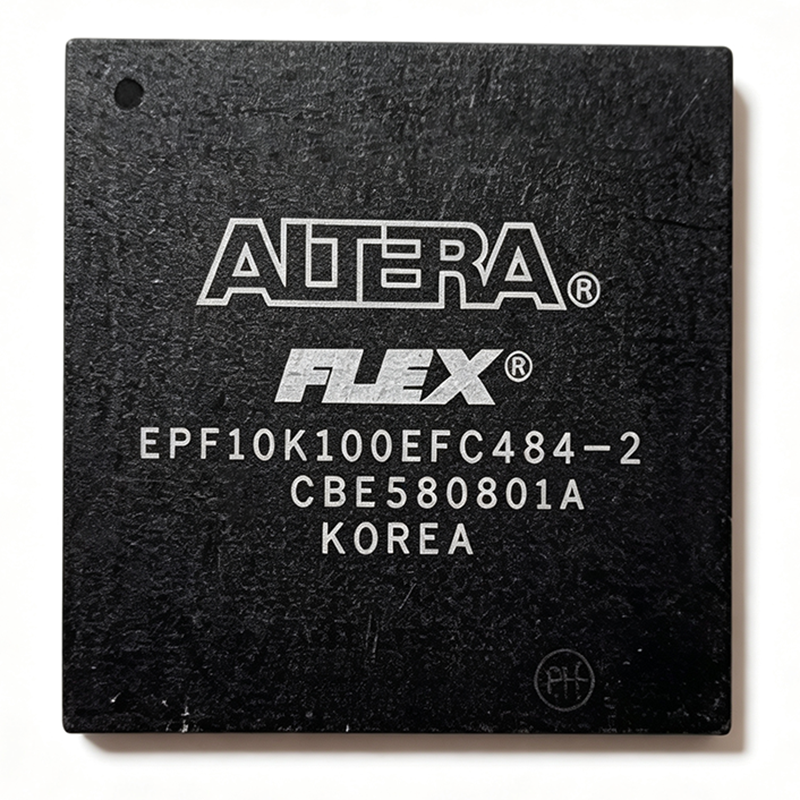
The EPF10K100EFC484-2 is an Altera (Intel) FLEX-10KE family SRAM-based FPGA delivering 49,992 logic elements across 624 LABs, 338 user I/O pins, and a 2.375 V to 2.625 V core supply in a 484-ball FineLine BGA (23 x 23 mm) package. The -2 speed grade offers moderate performance for cost-sensitive embedded and industrial designs. The part is in NRND (Not Recommended for New Designs) status but remains widely available: XAIPART stocks it with MOQ 1, priced at $267.05 per unit at quantity 1, stepping down to $185.40 at quantity 1,000, as of 2026-09-12. This guide covers verified specifications, design-in practices, the pin-to-pin compatible EPF10K100EFC484-2N alternative, lifecycle considerations, and sourcing strategy for engineers maintaining FLEX-10KE-based systems.
What Exactly Is the EPF10K100EFC484-2 and What Does It Deliver?
The EPF10K100EFC484-2 belongs to the FLEX-10KE family, built on 0.22 um SRAM CMOS process technology with 5 ns SRAM-configurable logic elements. As an FPGA, it contains an array of configurable logic blocks, programmable interconnects, and I/O cells that you rewire after manufacturing to implement arbitrary digital logic. Because the fabric is SRAM-based, the device must be configured at every power-up via JTAG or an EPC configuration device (EPC1, EPC2, or EPC16 family).
Verified key specifications from the XAIPART product database:
| Parameter | Value |
|---|---|
| Manufacturer | Altera (Intel) |
| Family / Series | FLEX-10KE |
| Logic Elements | 49,992 |
| Logic Array Blocks (LABs) | 624 |
| User I/O | 338 |
| Core Supply Voltage | 2.375 V to 2.625 V |
| Speed Grade | -2 |
| Process Technology | 0.22 um SRAM CMOS |
| Configuration | SRAM - serial JTAG or EPC configuration device |
| I/O Standards | LVTTL, LVCMOS, PCI, SSTL |
| Package | 484-BBGA / 484-FBGA, 23 x 23 mm |
| Operating Temperature | 0°C to +70°C (commercial) |
| Mounting | Surface Mount |
The naming convention is meaningful: the FC suffix denotes the 484-pin FineLine BGA package variant, and the -2 suffix denotes the speed grade. The 338 I/O count is the distinguishing feature of the FC484 package versus the lower-I/O BC256 and QC208 options in the same family. Embedded array blocks (EABs) provide RAM and ROM functions, with each EAB configurable as 256 x 8, 512 x 4, 1024 x 2, or 2048 x 1 bits; the device contains twelve EABs providing approximately 24,576 RAM bits total, according to the FLEX 10KE family datasheet.
How Do You Design In and Use the EPF10K100EFC484-2 Correctly?
Designing with this FPGA requires attention to power delivery, configuration, I/O banking, and software toolchain.
Power supply design. The core supply (VCCINT) requires 2.375 V to 2.625 V. Decouple the 2.5 V core with 0.1 uF and 10 uF capacitors placed close to the VCCINT pins. Separate VCCIO rails support multiple I/O standards; for 3.3 V PCI compliance, VCCIO must be tied to 3.3 V.
Configuration. Because the fabric is SRAM-based, the device must be reconfigured at every power-up. Supported methods are serial JTAG, EPC configuration devices (EPC1, EPC2, EPC16), and passive serial/parallel configuration modes. Route configuration clocks away from switching signals to avoid JTAG programming errors. Configuration time depends on the data width (serial vs. parallel).
Design software. The EPF10K100EFC484-2 is supported by Altera Quartus II versions up to 13.0sp1, the final legacy release for FLEX 10KE devices. MAX+PLUS II also supports older designs, but new work should use Quartus II with the legacy device library for synthesis, place-and-route, and bitstream generation.
PCB layout. The fine-pitch 484-ball FineLine BGA uses a 22 x 22 ball grid (excluding depopulated center rows), with ball A1 as the top-left reference and rows lettered A through Y, columns numbered 1 through 22. The full pin-to-signal mapping is in the dsf10ke.pdf datasheet. Controlled-impedance routing on the BGA breakout supports signal integrity for 50 MHz LVTTL bus operation. Reflow profiling and careful via-in-pad or dog-bone breakout strategies are required; this raises NRE cost versus QFP-package CPLDs but buys far more I/O.
Capacity planning. The 624 LABs and 49,992 logic elements suit state-machine-intensive designs of roughly 20K-50K gate-equivalent complexity. The 338 I/O supports wide parallel buses, and the twelve EABs implement FIFOs, dual-port RAM, and distributed-arithmetic DSP structures.
What Are the Drop-In Alternatives and How Do They Compare?
Based on the verified alternative data, only two pin-compatible options exist within the same family:
| Parameter | EPF10K100EFC484-2 | EPF10K100EFC484-2N | EPF10K200EFC484-2 |
|---|---|---|---|
| Family | FLEX-10KE | FLEX-10KE | FLEX-10KE |
| Package | 484-FBGA | 484-FBGA (identical) | 484-FBGA (same) |
| Speed Grade | -2 | -2 | -2 |
| Logic / Gates | 100K typical gates (49,992 LEs) | Same die, same 49,992 LEs | 200K gates, 2x logic density |
| Terminal Finish | [DATA_NEEDED: terminal finish] | Lead-free / RoHS-compliant | [DATA_NEEDED: terminal finish] |
| Compatibility | Reference part | Pin-to-pin compatible, same PCB footprint | Pin-compatible but logic footprint differs |
The EPF10K100EFC484-2N is the best drop-in replacement: identical die, package, 49,992 logic elements, and -2 speed grade. Per DigiKey listings, the only functional difference is the lead-free terminal finish; electrically and mechanically the two parts are drop-in compatible on the same PCB footprint, making the -2N the correct choice when RoHS compliance is mandatory. The EPF10K200EFC484-2 doubles logic density (200K vs 100K gates) in the same package and speed grade; it is pin-compatible at the package level but requires design changes since the logic footprint differs. Note that migration to modern Intel devices (MAX II, MAX V, Cyclone IV) is generally NOT pin-to-pin; a PCB redesign is typically required, according to Intel's legacy device migration guidance.
Where Is This FPGA Used? Six Verified Application Scenarios
The high I/O count and moderate logic density map to six practical use cases, each anchored to verified specifications:
1. Industrial control glue logic. The 49,992 logic elements and 338 I/O consolidate dozens of 74-series logic functions into one programmable device, handling state machines, motor-control timing, and sensor-signal routing. JTAG in-circuit programming allows field reconfiguration. Trade-off: higher per-unit cost than discrete logic, offset by smaller PCB area and lower BOM count.
2. Telecommunications line-card interface. The 338 user I/Os accept wide parallel TDM buses (H.110, MVIP, SCSA), while the 624 LABs implement cell/packet reassembly. The 2.5 V core draws typical 0.5 W to 1.5 W, and the FC484 BGA provides controlled-impedance signal integrity for 50 MHz LVTTL buses.
3. Legacy PCI bus bridge controller. The device implements 33 MHz / 32-bit PCI target or master state machines, with the twelve EABs providing FIFOs for posted-write and read-completion buffering. VCCIO tied to 3.3 V supports PCI signaling. Remember: an on-board EPC configuration device is required because SRAM configuration is lost at power-down.
4. Embedded DSP co-processor. EAB-based dual-port RAM supports distributed-arithmetic FIR filters and FFT butterflies running in parallel at -2 speed grade clock rates, offloading kernels from a host CPU via short bus traces enabled by the 484-FBGA placement near the processor.
5. Test and measurement signal conditioning. Pattern generators, custom trigger sequencers, and protocol-aware formatters benefit from JTAG-rewritable fabric and deterministic parallel I/O timing, interfacing with 16-bit ADCs/DACs while EABs buffer sample bursts.
6. Factory automation sensor aggregation. The 338 I/Os simultaneously sample dozens of digital sensors (proximity, photoelectric, encoders, limit switches); LVCMOS/LVTTL I/O banks integrate with 3.3 V and 5 V sensor networks via level shifters, and JTAG ISP enables late customization during commissioning.
What Is the Lifecycle Status and Supply Situation?
The EPF10K100EFC484-2 carries NRND (Not Recommended for New Designs) status per current Altera (Intel) lifecycle information. The FLEX-10KE family has been superseded by the Cyclone and MAX series; long-term production continuity is maintained through Rochester Electronics and remaining distributor inventory rather than new wafer runs. Authorized distributors currently stocking the part include DigiKey, Mouser, Heisener, and Rochester Electronics; Heisener lists 7,984 pieces in stock with typical lead times of 5-7 business days (as of 2026-09-11). XAIPART itself shows 99,999 units in stock with MOQ 1 as of 2026-09-12. For designs already in production, this means sourcing remains viable today, but buyers should secure long-term allocation or qualify the -2N variant now rather than waiting for distributor inventory to erode.
What Should Buyers Watch: Pricing, Trends, and Outlook?
Pricing. Verified XAIPART tier pricing as of 2026-09-12: $267.05 at qty 1, $248.50 at qty 10, $220.00 at qty 100, $198.75 at qty 500, and $185.40 at qty 1,000. The volume discount from qty 1 to qty 1,000 is roughly 30.6%, so consolidating annual demand into fewer, larger purchases materially reduces unit cost.
Trends to watch:
- RoHS pressure favors the -2N. If your product must meet lead-free requirements, standardize on the EPF10K100EFC484-2N, which is drop-in compatible; verify your reflow profile suits the lead-free terminal finish.
- Shrinking legacy toolchain window. Quartus II 13.0sp1 is the final legacy release supporting FLEX 10KE. Maintain archived tool installations and bitstream sources now, since future OS updates may make legacy toolchains harder to run.
- Configuration device pairing. Every shipped unit needs an EPC1/EPC2/EPC16 configuration device or JTAG load path; secure these companion parts alongside the FPGA, as legacy configuration devices face the same lifecycle pressures.
- Plan the migration horizon. For new designs, Intel recommends MAX II or MAX V CPLDs for equivalent logic density, or Cyclone IV FPGA fabric when embedded multipliers are required, but budget a PCB redesign since cross-generation drop-in replacement is not possible.
- Verify specs before order commitment. Total embedded memory bits summary and RoHS status of the base -2 part are not published in the summary data; confirm via the dsf10ke.pdf datasheet before finalizing BOMs. [VERIFY_NEEDED: RoHS compliance of EPF10K100EFC484-2 base variant]
Bottom line. For sustaining engineering on existing FLEX-10KE platforms, the EPF10K100EFC484-2 remains a fully sourced, spec-verified option at $267.05 (qty 1) down to $185.40 (qty 1,000) as of 2026-09-12, with the pin-identical, RoHS-compliant -2N variant as the forward-looking substitution choice.
Comments
Be the first to comment.
🔐 Please sign in to post a comment.
Don't have an account? Sign up