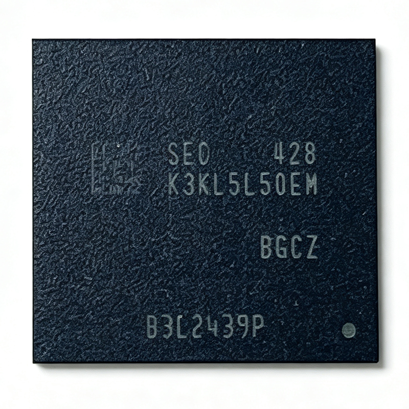
Quick Answers: What Is the K3KL4L40EM-BGCU 12 GB LPDDR5X DRAM?
The Samsung K3KL4L40EM-BGCU is a 96 Gbit (12 GB) LPDDR5X ultra-low-power mobile DRAM that drives an x64 bus at up to 8,533 Mbps from a 496-ball FBGA surface-mount package. It is the 12 GB density tier of Samsung's LPDDR5X family, positioned between the 64 Gbit K3KL3L30DM-BGCU and the 128 Gbit K3KL5L50DM-BGCU, which share the same 496-ball footprint and the same 8,533 Mbps speed grade. Lifecycle status is active. XAIPART holds 99,999 units with an MOQ of 1, and volume pricing reaches $73.1818 per unit at the 1,000-piece tier as of 2026-09-16. The device targets smartphones, tablets, and wearables, and it also fits edge-AI and high-performance embedded compute modules built on Qualcomm Snapdragon or MediaTek Dimensity application processors.
| Verified Parameter | K3KL4L40EM-BGCU Value |
|---|---|
| Memory type | LPDDR5X DRAM (LPDDR5 JEDEC-based interface) |
| Density | 96 Gbit (12 GB) |
| Bus organization | x64 |
| Maximum data rate | 8,533 Mbps |
| Package | 496-ball FBGA, surface mount |
| Storage class | Volatile memory (DRAM) |
| Power characteristic | Ultra-low-power mobile DRAM |
| Companion densities | 64 Gbit K3KL3L30DM-BGCU, 128 Gbit K3KL5L50DM-BGCU |
| Core supply voltage (VDD) | [DATA_NEEDED: core supply voltage (VDD)] |
| Operating temperature | [DATA_NEEDED: operating temperature range] |
| RoHS status | Unknown in XAIPART records [VERIFY_NEEDED: RoHS compliance certificate] |
| Lifecycle status | Active |
| XAIPART stock | 99,999 units, MOQ 1 |
| Unit price at 1,000 pcs | $73.1818 as of 2026-09-16 |
The one-line buying answer: this is a current-generation 12 GB mobile DRAM in stock at MOQ 1, priced on a steep volume curve, and footprint-compatible with the 8 GB and 16 GB members of the same Samsung LPDDR5X family. The engineering answer: it is a bandwidth-first part, and the design work sits in channel routing, controller compatibility, and BOM-tier planning rather than in schematic capture.
Technical Guide: How Do You Design In the K3KL4L40EM-BGCU?
Designing in an 8,533 Mbps LPDDR5X device is a channel-design exercise as much as a memory-selection exercise. The K3KL4L40EM-BGCU places 96 Gbit of volatile storage behind a 64-bit bus, so the engineering effort concentrates on six areas: density planning, bandwidth budgeting, signal integrity, supply and controller compatibility, memory training, and mechanical plus compliance closure.
Step 1 — Fix the Density Tier Before You Route
Samsung builds the 64 Gbit K3KL3L30DM-BGCU, the 96 Gbit K3KL4L40EM-BGCU, and the 128 Gbit K3KL5L50DM-BGCU on a common 496-ball FBGA footprint at a common 8,533 Mbps speed grade. Capacity therefore becomes a bill-of-materials decision rather than a layout decision. A platform team can define a 12 GB single-package design and later add 8 GB or 16 GB SKUs without a PCB respin, as long as the SoC memory-compatibility list covers the chosen density and die revision.
Capacity arithmetic for planning: 1 × K3KL4L40EM-BGCU = 96 Gbit = 12 GB; 2 × K3KL4L40EM-BGCU = 192 Gbit = 24 GB [derived from verified density = 96 Gbit].
Step 2 — Build the Bandwidth Budget
Peak theoretical bandwidth per device = 8,533 Mbps × 64 bits = 546,112 Mbps ≈ 546.1 Gbit/s ≈ 68.26 GB/s [derived from verified data rate = 8,533 Mbps and organization = x64]. Delivered throughput sits below that after refresh, training, and read/write turnaround overhead, so budget against your SoC vendor's efficiency model rather than against the raw number.
The commercial comparison that matters is LPDDR5X versus LPDDR5. At 8,533 Mbps this part runs roughly 33% faster than the 6,400 Mbps LPDDR5 ceiling described in the product data, and it does so with ultra-low-power mobile DRAM efficiency, which raises bandwidth-per-watt — the dominant design metric in mobile SoC platforms.
Step 3 — Enforce Signal-Integrity Discipline at 8,533 Mbps
The product data is explicit on this point: LPDDR5X signal integrity at 8,533 Mbps demands strict length-matched routing, controlled impedance, and adherence to the SoC vendor's reference layout guidelines. The point-to-point links typical of mobile layouts are short, so via stubs, impedance discontinuities, and reference-plane splits eat the eye budget quickly. Treat the reference layout as a hard requirement, not a starting suggestion.
Step 4 — Close Out Supply and Controller Support
Core supply voltage (VDD) is [DATA_NEEDED: core supply voltage (VDD)] and the operating temperature range is [DATA_NEEDED: operating temperature range]. Both values must come from the current Samsung datasheet before the power tree is frozen, because LPDDR5X rail design and PMIC selection depend on them.
On the controller side, this device requires an application processor and PMIC pair that explicitly support the LPDDR5X speed and voltage profiles. LPDDR5X extends the JEDEC LPDDR5 standard; a controller that tops out at LPDDR5 rates cannot run the K3KL4L40EM-BGCU at 8,533 Mbps.
Step 5 — Plan Memory Training and Second-Sourcing Early
LPDDR5X behavior is controller-dependent: boot-time calibration, die-revision handling, and training parameters live in the SoC vendor's supported-memory list. Treat that list as a release gate. The same dependency explains why cross-brand substitution is not a pin swap — SK Hynix and Micron 96 Gbit-class LPDDR5X devices exist in 496-ball packages, but package ballouts and memory-training parameters are controller-dependent, and no pin-compatible cross-brand equivalent for the K3KL4L40EM-BGCU is published in available cross-reference data.
Step 6 — Close Mechanical, Thermal, and Compliance Items
The 496-ball FBGA is a surface-mount, fine-pitch BGA package that requires standard fine-pitch BGA reflow practice [VERIFY_NEEDED: exact reflow profile from the Samsung datasheet]. RoHS status is recorded as unknown in XAIPART data, so request compliance documentation with the shipment [VERIFY_NEEDED: RoHS compliance certificate]. Teams building automotive cockpit or ADAS compute modules should note that this is a mobile-grade component: the standard consumer part must be evaluated against the project's AEC-Q100 requirements before it is designed in, and Samsung's automotive-qualified LPDDR variants should be considered for those programs.
Alternatives & Comparison: Which LPDDR5X Parts Are Drop-In Alternatives to the K3KL4L40EM-BGCU?
Drop-in candidates come from inside the same Samsung LPDDR5X family, because those are the only parts documented in this dataset as sharing the 496-ball FBGA footprint and the 8,533 Mbps speed grade. The table below compares the K3KL4L40EM-BGCU against its documented companions using verified specification values only.
| Parameter | K3KL4L40EM-BGCU | K3KL4L40DM-BGCU | K3KL3L30DM-BGCU | K3KL5L50DM-BGCU |
|---|---|---|---|---|
| Memory type | LPDDR5X DRAM | LPDDR5X DRAM (Samsung family) | LPDDR5X DRAM (Samsung family) | LPDDR5X DRAM (Samsung family) |
| Density | 96 Gbit (12 GB) | 96 Gbit (12 GB) | 64 Gbit (8 GB) | 128 Gbit (16 GB) |
| Bus organization | x64 | x64 | x64 | x64 |
| Maximum data rate | 8,533 Mbps | 8,533 Mbps | 8,533 Mbps | 8,533 Mbps |
| Interface | LPDDR5X (LPDDR5 JEDEC-based) | LPDDR5X | LPDDR5X | LPDDR5X |
| Package | 496-ball FBGA | 496-ball FBGA | 496-ball FBGA | 496-ball FBGA |
| Drop-in status on the same footprint | Baseline device | Yes — same density, same speed; earlier package/process generation variant | Yes — lower density | Yes — higher density, subject to SoC support |
| Primary selection driver | 12 GB per socket with maximum bandwidth | Same density, alternate die/process generation | Lower cost per socket at 8 GB | Maximum capacity per package at 16 GB |
The closest substitute is the K3KL4L40DM-BGCU: identical 96 Gbit density, identical 8,533 Mbps rate, identical x64 organization, and the -DM suffix denotes an earlier package/process generation variant of the same density-and-speed family rather than a different function. Before substituting it, confirm die revision compatibility and firmware or training settings against the SoC vendor's memory compatibility list.
For density-driven substitution, the decision is economic and architectural rather than electrical. Choose the K3KL3L30DM-BGCU when 8 GB per device is sufficient and cost per socket matters; choose the K3KL5L50DM-BGCU when 16 GB per package is required and the memory controller supports the higher density. Both retain the 496-ball FBGA footprint, so signal-integrity design carries over unchanged.
Cross-brand alternatives are a different category. SK Hynix and Micron both offer 96 Gbit-class LPDDR5X devices in 496-ball packages with 8,533 Mbps support, but no pin-compatible equivalent is published in available cross-reference data, and substitution requires SoC vendor qualification plus board-level validation [VERIFY_NEEDED: SK Hynix / Micron cross-reference confirmation].
Industry Insight: What Is the Market and Supply Position of the K3KL4L40EM-BGCU?
Lifecycle status is active, which matters for long-lived designs: this is a current production device, not an end-of-life allocation buy. XAIPART lists 99,999 units in stock with an MOQ of 1, so prototyping and pre-production builds do not require a volume commitment.
| Quantity Tier | Unit Price (USD, as of 2026-09-16) |
|---|---|
| 1+ | $125.4545 |
| 10+ | $90.6061 |
| 100+ | $80.1515 |
| 500+ | $76.6667 |
| 1,000+ | $73.1818 |
The price curve carries a procurement signal. Unit cost declines approximately 41.6% between the 1-piece tier and the 1,000-piece tier [derived from verified tier pricing]. That shape is characteristic of high-volume mobile DRAM: the part is built for design-in and ramp, not for catalog spot buys, so allocation conversations belong in the design phase rather than the production phase.
Broker-channel availability has fluctuated as expected for mobile DRAM. Third-party listings reported 33,840 pcs in stock at Wolfchip, updated Aug 26, 2026, with immediate shipment, and Element (Hong Kong) Technology has also listed the part; DRex Electronics accepts RFQ submissions for quantity and target price. Because LPDDR5X components are sold primarily into high-volume mobile manufacturing, most availability runs through RFQ-based channels rather than fixed catalog pricing, and buyers should present quantity plus delivery schedule to get current market quotes.
Supply risk deserves explicit treatment. LPDDR5X parts are common targets for remarked or counterfeit supply, so request freshness and lot-date documentation with every order and qualify incoming material against a defined inspection plan [VERIFY_NEEDED: incoming inspection plan for LPDDR5X authenticity].
Positioned competitively, this device sits in the volatile memory class that acts as main system memory in mobile SoC platforms, alongside application processors where bandwidth-per-watt is the dominant metric. Published market-share or shipment data for the LPDDR5X segment is [DATA_NEEDED: LPDDR5X market share / unit shipment data].
Trends & Outlook: What Should LPDDR5X Buyers Watch?
Four dynamics, all anchored to verified specifications, drive sourcing and design decisions for this part through the current product cycle.
- Bandwidth ceiling migration from LPDDR5 to LPDDR5X. The 8,533 Mbps data rate is roughly 33% above the 6,400 Mbps LPDDR5 ceiling documented in the product data. Expect new flagship platform designs to specify LPDDR5X-class memory and to reserve LPDDR5 for cost-tiered SKUs — which means the K3KL4L40EM-BGCU competes against LPDDR5 on bandwidth-per-watt, not on absolute price.
- Capacity scaling without respins. The shared 496-ball FBGA footprint and common 8,533 Mbps speed grade across the 64, 96, and 128 Gbit family members let one PCB serve 8 GB, 12 GB, and 16 GB SKUs. Buyers should expect suppliers to quote the family as a group, and should lock the density decision to the SoC compatibility list rather than to availability of a single suffix.
- On-device AI raising the memory floor. Transformer inference and NPU workloads are bandwidth-bound and capacity-hungry; 12 GB per package, or 24 GB across two packages, keeps larger quantized models resident instead of paging to storage. Watch the memory capacity specified by Qualcomm Snapdragon and MediaTek Dimensity class platforms, because that sets the demand baseline for this density tier.
- Second-sourcing discipline tightening. Cross-brand LPDDR5X substitution requires SoC vendor qualification and board-level validation, not a pin swap. Buyers should secure die-revision and training-parameter confirmation in writing before approving any alternative source.
Two documentation items remain open and should be resolved before a production release: core supply voltage (VDD) and the operating temperature range are not present in the verified dataset, and RoHS status is recorded as unknown. Obtain these from the current Samsung datasheet and supplier compliance documentation, then cross-check them against the SoC vendor's supported-memory list before finalizing the memory subsystem.
Comments
Be the first to comment.
🔐 Please sign in to post a comment.
Don't have an account? Sign up