What Is the LM2904QDRQ1 and Why Do Automotive Engineers Choose It?
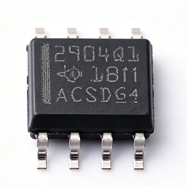
The Texas Instruments LM2904QDRQ1 is an automotive-grade dual operational amplifier qualified to AEC-Q100, operating from a single 3V to 26V supply (or dual supplies of ±1.5V to ±13V) with a 700 kHz gain-bandwidth product in an 8-pin SOIC (D) package rated -40C to +125C. It integrates two independent, internally compensated amplifiers with a typical 2 mV input offset voltage, 20 nA typical input bias current, and only 500 uA supply current per amplifier, with an input common-mode range that includes ground for true single-supply operation. On XAIPART, the part is in stock at 99,999 units with MOQ of 1, priced from $0.32 per unit down to $0.22 at 1,000 pieces as of 2026-09-04 (LM2904QDRQ1 product page).
A dual op amp packages two amplifiers in one SOIC-8 footprint, cutting board space and BOM cost for multi-channel signal conditioning. The bipolar process of the LM2904QDRQ1 delivers predictable, well-understood behavior: it is unity-gain stable with internal frequency compensation, includes output short-circuit protection, and swings its output close to the negative rail (though it is not rail-to-rail). ESD protection exceeds 500 V per MIL-STD-883 Method 3015 (HBM) and 200 V on the machine model, per the TI datasheet.
The 26V maximum supply rating is the headline feature for vehicle applications: it lets the amplifier connect directly to a 12V automotive battery rail while retaining load-dump headroom, eliminating a supply regulator stage in cost-sensitive modules. Add AEC-Q100 qualification and the -40C to +125C range, and the LM2904QDRQ1 becomes a default choice for body electronics, sensor conditioning, and powertrain-adjacent circuits.
What Are the Key Verified Specifications of the LM2904QDRQ1?
| Parameter | Value (verified) |
|---|---|
| Number of channels | 2 |
| Supply voltage (single) | 3 V to 26 V |
| Supply voltage (dual) | ±1.5 V to ±13 V |
| Gain-bandwidth product | 700 kHz (typ) |
| Slew rate | 0.3 V/us (typ) |
| Input offset voltage | 2 mV (typ), 7 mV (max) |
| Input bias current | 20 nA (typ) |
| Supply current per amplifier | 500 uA (typ) |
| Common-mode input range | Includes ground (V-) |
| Output swing | Close to negative rail; not rail-to-rail |
| ESD (HBM) | Exceeds 500 V (MIL-STD-883 Method 3015) |
| ESD (MM) | 200 V |
| Automotive qualification | AEC-Q100 qualified |
| Operating temperature | -40C to +125C |
| Package / mounting | SOIC-8 (D), surface mount |
| Protection / compensation | Output short-circuit protection; internal frequency compensation |
Source: TI LM2904-Q1 datasheet (ti.com/lit/ds/symlink/lm2904-q1.pdf), accessed 2026-09-04.
What Is the LM2904QDRQ1 Pinout in SOIC-8?
The LM2904QDRQ1 uses the industry-standard dual op amp SOIC-8 pinout shared with the LM358/LM2904 family, which is exactly why drop-in replacement across brands works so easily:
| Pin | Name | Function |
|---|---|---|
| 1 | OUT A | Amplifier A output |
| 2 | IN A- | Amplifier A inverting input |
| 3 | IN A+ | Amplifier A non-inverting input |
| 4 | V- / GND | Negative supply or ground (single supply) |
| 5 | IN B+ | Amplifier B non-inverting input |
| 6 | IN B- | Amplifier B inverting input |
| 7 | OUT B | Amplifier B output |
| 8 | V+ | Positive supply (3V to 26V) |
Source: TI LM2904-Q1 datasheet, verified against the XAIPART database pinout table.
How Do You Design In the LM2904QDRQ1 Correctly?
Power and decoupling. Connect pin 8 (V+) to a rail anywhere from 3V to 26V and pin 4 to ground or the negative dual-supply rail. Place a 0.1 uF ceramic capacitor close to pin 8. The design tip from the TI datasheet application guidance is simple but frequently skipped — long decoupling loops on a battery-connected rail invite transient-induced misbehavior.
Input common-mode discipline. Keep the input common-mode below VCC − 1.5V. The common-mode range extends down to and includes the negative rail, which is what enables ground-referenced, single-supply sensing — but the upper side has headroom limits. Exceeding it causes the classic phase-reversal-free but non-linear behavior at the upper range boundary.
Offset budgeting. With 2 mV typical and 7 mV maximum input offset, budget error early. On a 50 mV full-scale shunt, 2 mV is 4% of span typical (14% worst case at 7 mV max). Buffer high-impedance sources to limit offset errors, and remember the 20 nA typical bias current flows through your source impedance — a 100 kΩ source resistor adds 2 mV of error at the input.
Bandwidth and slew. The 700 kHz GBW supports closed-loop gains of 10 with roughly 70 kHz of bandwidth, which is ample for sensor loops, motor control (typically below 10 kHz), and active filters into the tens of kilohertz. The 0.3 V/us slew rate limits large-signal response — fine for audio-band and DC-accurate circuits, too slow for fast edges. In comparator duty, expect microsecond-scale response and add hysteresis.
Output behavior. The output swings close to the negative rail but is not rail-to-rail. Reserve headroom near the positive rail when mapping signal ranges to an ADC, and exploit the single-supply pull-down for near-0V low-level indications.
Stability. The part is internally compensated and unity-gain stable, and it remains stable with moderate capacitive loads. For Sallen-Key and multiple-feedback filter topologies, this makes it a straightforward choice without external compensation networks.
Worked Design Example: Low-Side Current Sense on a 12V Automotive Rail
Problem: Measure load current on a 12V battery rail across a low-side shunt and feed an MCU ADC, surviving -40C to +125C and automotive supply transients.
Approach: Use one LM2904QDRQ1 channel in a non-inverting configuration. The ground-including common-mode range lets pin 3 sit at the shunt's ground-referenced junction directly.
Calculations (using verified specs): A 10 mV full-scale shunt sits at the offset floor (2 mV typ / 7 mV max), so select a 50 mV full-scale shunt: 2 mV / 50 mV = 4% typical offset contribution, 14% worst case. For a 2.5 V ADC full-scale, set G = 50 V/V, so Rf/Rg = 49 (Rg = 1 kΩ, Rf = 49 kΩ). Closed-loop bandwidth = GBW / G = 700 kHz / 50 = 14 kHz. The 2.5 V output stays well within headroom below VCC = 12V, respecting the not-rail-to-rail output spec.
Results: One SOIC-8 device provides the gain channel plus a spare buffer or hysteresis-equipped comparator channel at 500 uA per amplifier, with 26V transient headroom and AEC-Q100 qualification. For shunts below about 10 mV full-scale, TI and XAIPART guidance recommends a dedicated current-sense amplifier such as the INA2181.
Which Components Are the Best Drop-In Alternatives to the LM2904QDRQ1?
| Part | Positioning | Key Differences (verified) | Drop-in? |
|---|---|---|---|
| TI LM2904BQDRQ1 | Next-generation die upgrade | 32V rating, tighter offset, higher ESD robustness; identical pinout | Yes — no PCB change |
| TI LM2904QDRG4Q1 | Same die, G4 packaging variant | RoHS/green suffix (G4); electrically the same die | Yes |
| TI LM2904VQDR | 32V variant | 32V max supply; not AEC-Q100 qualified; same SOIC-8 pinout | Pin-compatible; verify qualification needs |
| onsemi LM2904DR2G | Cross-brand equivalent | Standard grade, industry-standard SOIC-8 pinout, 26V-class | Pin-compatible; verify -Q1 qualification level |
| ST LM2904DT | Cross-brand equivalent | Standard grade; verify -Q1 qualification level | Pin-compatible; verify qualification |
How to choose: For new automotive designs that need 32V supply tolerance, tighter input offset, higher ESD robustness, or long-term supply continuity, choose the LM2904BQDRQ1 — TI positions it as the upgraded replacement. Keep the LM2904QDRQ1 for cost-sensitive designs already qualified at 26V, or to preserve form-fit-function continuity in existing production BOMs. If you substitute an onsemi or ST cross-brand part into an automotive program, verify the specific grade against each vendor's datasheet, because standard-grade LM2904 parts may not carry the -Q1 automotive qualification. Note also that the commercial LM358 (0C to +70C, no automotive qualification) is not acceptable in vehicle environments despite its near-identical electrical behavior and matching pinout; the LM2904QDRQ1 is the correct automotive pick.
Full specification detail and live stock for each part are on the LM2904QDRQ1 product page and the LM2904BQDRQ1 page in the Amplifier ICs category.
Where Does the LM2904QDRQ1 Fit in the Market, and How Is Supply?
Lifecycle status: active (verified from XAIPART product database). The LM2904-Q1 family is a long-standing, high-volume commodity part in TI's automotive analog portfolio; the introduction of the LM2904B-Q1 as a drop-in upgrade indicates TI's strategy of refreshing the die while preserving the pinout and footprint — a favorable signal for long-term continuity in either direction.
Supply situation: XAIPART lists 99,999 units in stock with MOQ of 1 as of 2026-09-04. Tiered pricing: $0.32 (1+), $0.29 (10+), $0.26 (100+), $0.24 (500+), $0.22 (1,000+), and $0.2202 (3,000+) as of 2026-09-04. The sub-$0.25 volume price is characteristic of a mature, multi-sourced commodity device. For automotive programs requiring PPAP documentation, source from authorized channels to guarantee traceability and TI warranty coverage. [DATA_NEEDED: manufacturer-announced lifecycle milestones and lead-time trends]
What Should Buyers and Engineers Watch Next?
Voltage margin migration. The verified family split is clear: the LM2904QDRQ1 tops out at 26V with 2 mV typical offset, while the LM2904BQDRQ1 raises supply tolerance to 32V, tightens offset, and improves ESD robustness on the identical pinout. For new automotive designs, the 32V margin part reduces risk against higher transient specs at essentially the same footprint and assembly cost.
Specification-fit discipline. Anchor decisions to the verified numbers: 700 kHz GBW, 0.3 V/us slew rate, 500 uA per amplifier, ground-including input common-mode, and a not-rail-to-rail output. These specs define the part's sweet spot — low-frequency, DC-accurate, single-supply conditioning — and its boundaries: precision sub-10 mV shunt sensing and fast comparison duty need dedicated devices such as the INA2181 or LM393DR.
Qualification audits. When cross-brand substitution enters a bill of materials, confirm the -Q1 qualification explicitly against each vendor's datasheet. The same SOIC-8 pinout across TI, onsemi, and ST parts simplifies layout reuse, but automotive compliance documentation requires the qualified ordering code.
Pricing watch. At $0.22 per 1,000 (as of 2026-09-04) with deep stock on XAIPART, the LM2904QDRQ1 remains among the lowest-cost AEC-Q100 paths to dual-channel amplification; commodity op amp prices fluctuate with volume, so lock tiered pricing during design freeze. Download the latest revision of the official TI PDF (ti.com/lit/ds/symlink/lm2904-q1.pdf) before finalizing safety-related ratings.
Comments
Be the first to comment.
🔐 Please sign in to post a comment.
Don't have an account? Sign up