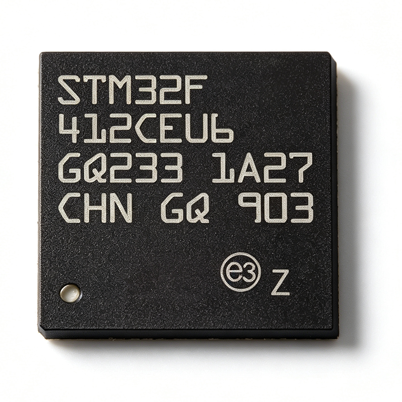
What Is the STM32F412CEU6 and Why Should Engineers Care?
The STM32F412CEU6 is a high-performance 32-bit microcontroller from STMicroelectronics, built around an ARM Cortex-M4F core running at up to 100 MHz with a single-precision floating-point unit (FPU) and DSP instructions. It combines 512 KB of flash memory, 128 KB of SRAM, and a rich peripheral set — including 4 USARTs, 3 SPIs, 3 I2Cs, a USB 2.0 OTG full-speed interface, a 12-bit ADC with 16 channels, a 12-bit DAC with 2 channels, 8 timers, and a true random number generator (RNG) — all in a compact UFQFPN-48 (7x7 mm) package. It operates from a 1.7 V to 3.6 V supply across an industrial temperature range of -40 °C to +85 °C, and it is RoHS compliant.
As of 2026-09-14, the STM32F412CEU6 is in active lifecycle status with 99,999 units in stock on XAIPART's STM32F412CEU6 product page, priced from $6.50 for single units down to $4.16 at 1,000-unit quantities, with MOQ of 1. That combination of verified availability, deep memory, and hardware floating-point makes it a strong choice for industrial control, IoT gateways, motor drives, audio processing, consumer electronics, and test-and-measurement designs where board space is tight but processing headroom matters.
The device is fabricated on a 90 nm process, balancing performance against power consumption. It provides Sleep, Stop, and Standby low-power modes, a nested vectored interrupt controller (NVIC) for efficient interrupt handling, and a memory protection unit (MPU) for application security. An FSMC external memory interface allows expansion beyond internal flash and SRAM when your application outgrows on-chip memory.
How Do You Select and Design In the STM32F412CEU6?
Designing in the STM32F412CEU6 starts with matching its verified capabilities to your system requirements. Confirm that 512 KB of flash and 128 KB of SRAM cover your firmware footprint, that the 100 MHz Cortex-M4F with FPU delivers the compute performance you need (125 DMIPS per the datasheet), and that the 36 GPIO pins and peripheral set — 4 USARTs, 3 SPIs, 3 I2Cs, USB 2.0 OTG FS, and FSMC — satisfy your connectivity budget.
Power Supply Design
The MCU operates from a single 1.7 V to 3.6 V supply, which directly supports 3.3 V logic systems and battery-powered designs. Follow these verified layout guidelines from the product data: decouple each VDD pin with 100 nF capacitors placed close to the pin, and add a 4.7 µF bulk capacitor on the supply rail. Connect VDDA to a clean analog supply and VREF+ to a stable reference voltage to preserve the accuracy of the 12-bit ADC and 12-bit DAC.
Boot Configuration
BOOT0 (pin 40) and BOOT1 (PB2, pin 13) select the boot mode among flash, system memory, and SRAM. Pull BOOT0 low for normal flash execution; use system memory boot for programming over the built-in bootloader during development. Verify your strap resistors before production to avoid unintended boot modes.
Key Pin Assignments for Hardware Engineers
From the verified pinout, the most important functional pins include:
| Pin | Name | Function |
|---|---|---|
| 1, 16, 32 | VDD | Power supply (decouple each with 100 nF) |
| 6, 24, 43 | VSS | Ground |
| 27 | NRST | Reset |
| 40 | BOOT0 | Boot mode selection |
| 13 | PB2 / BOOT1 | Boot mode selection |
| 4, 5 | PA2, PA3 | USART2 TX/RX |
| 45, 46 | PA9, PA10 | USART1 TX/RX |
| 47, 48 | PA11, PA12 | USB DM / DP (USB 2.0 OTG FS) |
| 38, 39 | PB6, PB7 | I2C1 SCL/SDA |
| 35, 9, 10 | PB3, PA6, PA7 | SPI1 SCK/MISO/MOSI |
| 7, 8 | PA4, PA5 | DAC output channels 1 and 2 |
| 25, 26 | PH0, PH1 | Main oscillator in/out |
The full 48-pin table lives on the product page.
Peripheral Budgeting
With 8 timers including advanced timers with dead-time generation, the STM32F412CEU6 directly supports PWM motor-control topologies such as six-step and field-oriented control (FOC). The 12-bit ADC with 16 channels provides sufficient inputs for multi-phase current sensing plus position feedback. For signal chains, use the 2-channel 12-bit DAC for analog references or audio output, and the I2S-capable serial interfaces for external audio codecs.
Firmware Considerations
The Cortex-M4F core executes DSP instructions natively, so filter kernels, FFTs, and FOC math benefit from the FPU without fixed-point conversion effort. The MPU lets you partition memory for safety-critical tasks, and the RNG supports encryption key generation for secure IoT communications.
Which Components Are Drop-In Alternatives to the STM32F412CEU6?
Only alternatives verified in the XAIPART database are listed below. The STM32F411CEU6 is a pin-compatible option in the same UFQFPN-48 package when USB OTG and RNG are not required; the STM32F412CEU6TR is the identical silicon in tape-and-reel packaging for automated assembly. Cross-brand pin-compatible drop-ins do not exist in the verified data — the NXP LPC4337FBD144 uses a different package and is not pin-compatible.
| Parameter | STM32F412CEU6 | STM32F412CEU6TR | STM32F412RGU6 | LPC4337FBD144 |
|---|---|---|---|---|
| Core | ARM Cortex-M4F @ 100 MHz | ARM Cortex-M4F @ 100 MHz (same die) | ARM Cortex-M4F, same core and memory | Dual-core Cortex-M4/M0 |
| Flash / SRAM | 512 KB / 128 KB | 512 KB / 128 KB | Same core and memory as F412CE | [DATA_NEEDED: flash and SRAM values] |
| Package | UFQFPN-48 (7x7 mm) | UFQFPN-48 (7x7 mm) | 64-pin (more GPIOs) | Different package, 144-pin |
| Pin-compatible with F412CEU6 | — | Yes (identical silicon) | No (different pin count) | No |
| Differentiators | USB 2.0 OTG FS, RNG | Tape-and-reel packaging | More GPIOs | Dual-core architecture |
| Drop-in replacement? | — | Yes | No | No |
Selection guidance: choose the STM32F412CEU6TR for automated assembly lines needing reel packaging; choose the STM32F412RGU6 when you need more GPIOs and can accept a 64-pin layout change; avoid the LPC4337FBD144 as a drop-in because it is not pin-compatible.
What Is the Market Position, Lifecycle Status, and Supply Situation for the STM32F412CEU6?
The STM32F412CEU6 is in active lifecycle status per the XAIPART product database, meaning STMicroelectronics continues to manufacture it and it is not approaching end-of-life. Supply is currently strong: 99,999 units are in stock on XAIPART as of 2026-09-14, with an MOQ of 1, so prototype and low-volume buyers can order single units without negotiating. [DATA_NEEDED: long-term lifecycle commitment date, market share data, and franchise distributor lead times — these are not provided in the verified dataset.] The database FAQ notes a typical lead time of 8–12 weeks for large orders, so production planners should forecast beyond in-stock quantities accordingly.
What Trends and Buying Signals Should You Watch for the STM32F412CEU6?
Three actionable signals, all anchored to verified specs:
1. Price breaks reward volume planning. Verified tiered pricing as of 2026-09-14 runs $6.50 (1+), $5.85 (10+), $5.20 (100+), $4.68 (500+), and $4.16 (1,000+) — a 36% unit-cost reduction from single-unit to 1,000-unit volume. Consolidating buys across project phases captures that spread while stock lasts.
2. The F412's USB OTG + RNG combination is a differentiator to preserve in BOM planning. If a cost-down migration is considered, the pin-compatible STM32F411CEU6 drops USB OTG and RNG. Designs relying on USB host/device connectivity or hardware-generated encryption keys must stay on the F412 family.
3. Package consolidation favors the 7x7 mm QFN footprint. With 36 GPIOs, USB, and FSMC in UFQFPN-48, the F412CEU6 lets teams standardize one 4-layer-friendly footprint across IoT, audio, and control products — reducing PCB respins when moving between family members.
Buyers should also monitor firmware-driven demand: the combination of DSP instructions, FPU, 512 KB flash, and 125 DMIPS performance keeps this part relevant for edge audio and motor-control workloads, which tends to sustain demand against the 99,999-unit current stock position.
Practical Design Example: BLDC Motor Drive on the STM32F412CEU6
Problem: Implement a closed-loop BLDC motor drive with field-oriented control (FOC) on a compact 3.3 V board.
Approach: Use the STM32F412CEU6's advanced timers to generate center-aligned PWM with dead-time insertion for the three-phase inverter. Sample two phase currents with the 12-bit ADC (two of the 16 channels), read the Hall or encoder feedback on GPIO/timer inputs, and run FOC math on the Cortex-M4F FPU at 100 MHz. Communicate with a host over USART or USB 2.0 OTG FS.
Design notes: Supply the MCU from a 3.3 V rail (within the verified 1.7–3.6 V range). Decouple each VDD pin with 100 nF close to the pin plus a 4.7 µF bulk capacitor; feed VDDA from a filtered analog supply so ADC current readings remain accurate. Strap BOOT0 low for flash boot.
Results: The verified peripheral set — advanced timers with dead-time generation, 12-bit ADC with 16 channels, FPU-accelerated 100 MHz core, and industrial -40 °C to +85 °C operation — covers the full signal and control chain for factory automation and robotics motor drives on a single 7x7 mm chip.
Where to Buy and Next Steps
The STM32F412CEU6 is available now on XAIPART with 99,999 units in stock and MOQ of 1 as of 2026-09-14. Download the official datasheet PDF from STMicroelectronics for full electrical characteristics, and review the XAIPART technical guides library for companion articles on STM32 firmware development and power-supply layout. For volume quotes above 1,000 units at the verified $4.16 tier, contact XAIPART sales.
Comments
Be the first to comment.
🔐 Please sign in to post a comment.
Don't have an account? Sign up