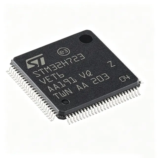
STM32H723VET6 Quick Answers: What Is This MCU and Why Does It Matter?
The STM32H723VET6 is a high-performance 32-bit microcontroller from STMicroelectronics built around an Arm Cortex-M7 core running at up to 550 MHz with a double-precision FPU. It integrates 1 Mbyte of flash memory, 564 Kbytes of SRAM, a 16-bit ADC sampling at up to 3.6 MSPS, a 12-bit DAC, and a cryptographic acceleration unit supporting AES, DES, and HASH. Connectivity includes Ethernet, USB OTG HS/FS, CAN FD, SPI, I2C, UART, and SDMMC. The device is housed in a 100-pin LQFP package (LQFP100) with a 14x14 mm body and 0.5 mm pitch, operates from a 1.62 V to 3.6 V supply, and is rated from -40°C to +125°C. As of 2026-08-30, the STM32H723VET6 is in stock at XAIPART with 99,999 units available, priced from $10.3636 for single units down to $6.0455 at 1,000 units, with an MOQ of 1 and lifecycle status: active.
This guide consolidates everything a buyer or design engineer needs: verified specifications, design-in practices for the LQFP100 package, pin-compatible alternatives, supply situation, and purchasing outlook. For current inventory and pricing, visit the STM32H723VET6 product page on XAIPART.
How Do You Select and Design In the STM32H723VET6?
Selecting the STM32H723VET6 makes sense when your application needs high real-time compute on a single chip. The 550 MHz Cortex-M7 core, with its 6-stage pipeline and branch prediction unit, executes control loops and DSP algorithms efficiently. The double-precision FPU accelerates floating-point math for audio processing, motor control, and industrial analytics. The memory protection unit (MPU) and cache controller enhance system reliability, while the 16-bit ADC with oversampling supports high-resolution data acquisition for precision measurement.
Key Verified Specifications
| Parameter | Value |
|---|---|
| Core | Arm Cortex-M7 |
| Maximum Clock Speed | 550 MHz |
| Flash Memory | 1 Mbyte |
| SRAM | 564 Kbytes |
| Package | LQFP100 (14x14 mm, 0.5 mm pitch) |
| Supply Voltage | 1.62 V to 3.6 V |
| Operating Temperature | -40°C to +125°C |
| ADC | 16-bit, 3.6 MSPS |
| DAC | 12-bit |
| Communication Interfaces | Ethernet, USB OTG HS/FS, CAN FD, SPI, I2C, UART, SDMMC |
| Timers | Multiple 16-bit and 32-bit timers |
| Cryptographic Acceleration | Yes (AES, DES, HASH) |
| GPIO Pins | Up to 82 |
| RoHS Status | Compliant |
Power Supply Design Best Practices
Proper power distribution is critical for reliable operation at 550 MHz. Decouple each VDD pin with 100 nF capacitors placed as close as possible to the pin. Filter the VDDA analog supply with a ferrite bead and a 1 µF capacitor to reduce analog noise, which directly protects the 16-bit ADC's effective resolution. The VCAP pins require a 2.2 µF capacitor each to stabilize the internal voltage regulator output. These layout practices come directly from the verified design guidance in the product database.
Clock and Layout Considerations
Careful attention to the crystal oscillator layout is essential for reliable clock generation. The LQFP100 provides dedicated OSC_IN and OSC_OUT pins (PH0/PH1 at pins 30-31) and 32.768 kHz oscillator pins (PC14/PC15 at pins 8-9 for OSC32_IN/OSC32_OUT). Keep oscillator traces short, guard them with ground pour, and keep them away from high-speed USB or Ethernet routing. For debug access, PA13 (SWDIO) and PA14 (SWCLK) on pins 94-95 provide the serial-wire debug interface, so expose these on a standard header in your PCB design.
Boot Configuration
BOOT0 (pin 76) selects the boot mode. Tie it low through a pulldown for normal flash boot, or provide a jumper to pull it high for system bootloader access during production programming.
Firmware Development
The verified FAQ notes the STM32CubeMX tool provides the STM32H723VET6 pinout for easy configuration, streamlining pin assignment and peripheral setup before layout begins. The datasheet PDF is available at st.com.
Which Drop-In Alternatives Can Replace the STM32H723VET6?
The STM32H723VET6 has several pin-compatible, same-package (LQFP100) alternatives within the STM32H7 family from STMicroelectronics. All are drop-in replacements at the hardware level, subject to firmware adjustments for differences in clock speed and memory.
| Parameter | STM32H723VET6 | STM32H743VIT6 | STM32H743VGT6 | STM32H753VIT6 | STM32H753VGT6 |
|---|---|---|---|---|---|
| Package | LQFP100 | LQFP100 | LQFP100 | LQFP100 | LQFP100 |
| Pin-Compatible | — | Yes | Yes | Yes | Yes |
| Max Clock Speed | 550 MHz | 480 MHz | 480 MHz | 480 MHz | 480 MHz |
| Flash Memory | 1 Mbyte | 2 Mbytes | 1 Mbyte | 2 Mbytes | 1 Mbyte |
| SRAM | 564 Kbytes | 1 Mbyte | 1 Mbyte | 1 Mbyte | 1 Mbyte |
Selection guidance: If you need maximum clock speed for compute-heavy real-time control, the STM32H723VET6 leads at 550 MHz. If your firmware outgrows 1 Mbyte of flash or 564 Kbytes of SRAM, the STM32H743VIT6 or STM32H753VIT6 double flash to 2 Mbytes and double SRAM to 1 Mbyte at the cost of a 480 MHz maximum clock. Because all four alternatives share the LQFP100 footprint, you can qualify a single PCB across multiple memory/speed variants and late-select the best-fit part. Browse XAIPART's STM32H7 series inventory via the microcontrollers category.
What Is the Market Position and Supply Situation for the STM32H723VET6?
The STM32H723VET6 carries an active lifecycle status from STMicroelectronics, indicating an ongoing production part suitable for new designs. As of 2026-08-30, XAIPART lists 99,999 units in stock with an MOQ of 1, meaning even prototype and low-volume buyers can source without volume commitments. Verified tiered pricing at XAIPART as of 2026-08-30 is $10.3636 (qty 1+), $7.4848 (qty 10+), $6.6212 (qty 100+), $6.3333 (qty 500+), and $6.0455 (qty 1,000+).
For broader distributor context, the database FAQ notes a typical lead time of 8-12 weeks from major distributors as of 2026-08-13. [DATA_NEEDED: current allocation status, franchise distributor stock levels, and manufacturer long-term availability commitment dates]
Where Does the STM32H723VET6 Deliver the Most Value in Real Applications?
The verified application data identifies six areas where this MCU's specification set maps directly to system requirements:
Industrial Control Systems
In PLC applications, the 550 MHz core manages multiple I/O points and executes real-time PID and motion-control loops, while the CAN FD interface supports robust industrial communication and the Ethernet MAC connects to HMI panels. The -40°C to +125°C range ensures reliability in harsh factory environments, and the cryptographic unit secures firmware updates.
Motor Drives
For field-oriented control (FOC) of BLDC motors, the 550 MHz core runs Clarke and Park transforms in real time, advanced timers generate precise PWM for the inverter stage, and the 16-bit ADC at 3.6 MSPS captures phase currents with the resolution needed for accurate torque control.
Audio Processing
The double-precision FPU handles real-time filtering, equalization, and compression. The 564 Kbytes of SRAM buffers audio samples to reduce latency, and the 12-bit DAC plus external codec connectivity (via I2S per the interface set) supports professional audio designs. [VERIFY_NEEDED: dedicated I2S peripheral detail beyond the listed interface set]
IoT Gateways
The Ethernet MAC and USB OTG interfaces enable network and peripheral connectivity, while the cryptographic acceleration unit (AES, DES, HASH) secures cloud-bound data. Sensors connect via SPI, I2C, or UART, and the wide temperature range suits outdoor installations.
Power Conversion
Digital power supplies, solar inverters, and battery chargers benefit from the 3.6 MSPS ADC for voltage/current monitoring and high-frequency PWM from the advanced timers. The 550 MHz core executes digital PID and predictive control to improve efficiency and transient response.
Medical Devices
Patient monitors and diagnostic equipment use the 16-bit ADC for high-resolution vital-sign acquisition, the cryptographic unit for secure data handling, and Ethernet/USB for hospital network integration during continuous clinical operation.
What Should Buyers Watch for in 2026-2027?
Anchor your purchasing decisions to these verified facts:
- Pricing leverage at volume: The step from single-unit ($10.3636) to 1,000-unit ($6.0455) pricing is a 41.7% reduction as of 2026-08-30. If your forecast supports it, consolidating orders above 500 units ($6.3333) captures most of the volume discount.
- Memory vs. speed trade: The pin-compatible family (H743/H753 variants) lets you trade 70 MHz of clock speed for up to double flash and SRAM. Design the PCB once, then optimize the BOM per firmware size.
- Lead-time planning: With 8-12 weeks typical lead time at major distributors (as of 2026-08-13), buffer stock or order against the production schedule rather than demand pull.
- Active lifecycle: The part is active and RoHS compliant, safe for new designs. Revisit the XAIPART product page for real-time stock updates before committing a production run.
- Security requirements: Hardware AES/DES/HASH acceleration is built in. If your roadmap adds secure boot or encrypted communication requirements, this device covers them without an external secure element. [VERIFY_NEEDED: secure boot feature specifics]
Practical Design Example: High-Resolution Motor Drive Control Loop
Consider a BLDC motor drive requiring precise torque control. The STM32H723VET6 reads phase currents through its 16-bit ADC at 3.6 MSPS — sufficient headroom for a fast inner current loop. The 550 MHz Cortex-M7 core with double-precision FPU executes the Clarke/Park transforms and current PI controllers, while advanced 16-bit/32-bit timers output the PWM signals to the gate drivers. The CAN FD interface links the drive to the supervisory controller, and the cryptographic unit secures command traffic. The wide -40°C to +125°C operating range supports industrial cabinet installations. This architecture uses only verified datasheet specifications and demonstrates why the H723's combination of clock speed, ADC performance, and timer resources is well suited to FOC implementations.
Comments
Be the first to comment.
🔐 Please sign in to post a comment.
Don't have an account? Sign up