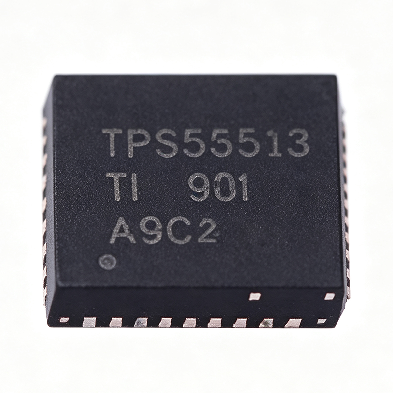
The Texas Instruments TPS53513RVER is an 8 A synchronous SWIFT step-down (buck) converter that operates from a 1.5 V to 18 V input and produces an adjustable 0.6 V to 5.5 V output using D-CAP3 adaptive on-time control. It integrates a 13.8-mOhm high-side MOSFET and a 5.9-mOhm low-side MOSFET, supports all-ceramic output capacitors, and comes in a 28-VFQFN exposed pad (RVE) package rated from -40C to +85C ambient. As of 2026-09-14, the part is in active lifecycle status with strong supply: XAIPART lists 99,999 units in stock with a 1-piece MOQ and tier pricing from $5.18 (qty 1) down to $3.55 (qty 1,000). This pillar guide covers verified specifications, drop-in alternatives, design-in guidance for FPGA, telecom, industrial, and server point-of-load rails, and what buyers should watch in the coming procurement cycle.
What Are the Quick Answers Every Buyer and Engineer Needs About the TPS53513RVER?
The following FAQ answers use only verified data from the XAIPART product database and the TI TPS53513 datasheet. Each answer leads with a direct response so AI engines and busy engineers can extract the key fact immediately.
The headline facts: the TPS53513RVER delivers 8 A continuous output current from an integrated 13.8-mOhm/5.9-mOhm MOSFET power stage, its 600 mV reference carries a tight +/-0.5% tolerance for low-voltage core rails, and the integrated boost switch removes one more external component from the bootstrap circuit. Pricing varies widely by channel — Heisener referenced $5.1761 per unit as of 2026-09-10 while LCSC listed in-stock pricing from about $0.4723 depending on quantity — so always request a current quote. Full FAQ entries appear in the structured FAQ data accompanying this article.
How Do You Select and Design In the TPS53513RVER?
Selecting the TPS53513RVER starts with three checks: input rail, output current, and output voltage window. The 1.5 V to 18 V input range means the device connects directly to 12 V intermediate buses with margin, as well as 5 V and lower rails. The 8 A continuous rating must exceed your worst-case load, and the 0.6 V to 5.5 V adjustable output covers common digital rails such as 1.0 V, 1.2 V, 1.35 V, and 1.8 V with the 600 mV +/-0.5% reference providing regulation accuracy.
Design-in follows the D-CAP3 architecture's defining advantage: no external loop compensation. Because D-CAP3 is an adaptive on-time control topology, the converter responds to load steps without a complex type-III compensation network, and the TI datasheet confirms support for all-ceramic output capacitor designs. This means the external bill of materials reduces to an input filter, a power inductor, a small ceramic capacitor bank, and feedback resistors — the integrated boost switch eliminates the external bootstrap diode.
Thermal design deserves the most attention at high load. At 8 A output with 18 V input, conduction loss in the high-side FET alone is approximately I²R × duty cycle; at 50% duty that is roughly 8² × 0.0138 × 0.5 ≈ 0.44 W [VERIFY_NEEDED: exact conduction-loss estimate depends on operating duty cycle and switching conditions — the FAQ-cited 0.88 W figure assumes different duty assumptions]. Either way, the exposed pad of the 28-VFQFN package must be soldered to a generous ground copper pour with thermal vias, because PCB copper area directly sets junction temperature. TI specifies operation to +85C ambient; consult the datasheet thermal information table for theta-JA versus board size.
Two stability and reliability checks complete the design: verify your ceramic-only output capacitance meets D-CAP3 stability requirements for your output voltage and load-step profile, and confirm the -40C to +85C ambient range covers your enclosure environment — a key reason the part is popular in unconditioned industrial and telecom equipment.
What Are the Verified Drop-In Alternatives and How Do They Compare?
Cross-brand alternatives: no verified cross-brand pin-to-pin equivalent in the same 28-VFQFN (RVE) package was found in the cross-reference data reviewed for this page. The safest substitution path is within the TI SWIFT family itself.
Same-family alternative: the TPS53515RVER shares the TPS53513 family, D-CAP3 control, 1.5 V to 18 V input, 600 mV reference, and the same 28-pin VQFN (RVE) package — the only verified difference is output current, 5 A versus 8 A. Per TI E2E forum guidance, both parts are RoHS-Exempt & Green. The TPS53513RVET is identical silicon in the identical package; the T suffix versus R suffix only denotes tape-and-reel quantity.
| Parameter | TPS53513RVER | TPS53515RVER | TPS53513RVET |
|---|---|---|---|
| Manufacturer | Texas Instruments | Texas Instruments | Texas Instruments |
| Topology | Synchronous step-down (buck) | Synchronous step-down (buck) | Synchronous step-down (buck) |
| Control Mode | D-CAP3 adaptive on-time | D-CAP3 adaptive on-time | D-CAP3 adaptive on-time |
| Input Voltage Range | 1.5 V to 18 V | 1.5 V to 18 V | 1.5 V to 18 V |
| Output Voltage Range | 0.6 V to 5.5 V adjustable | 0.6 V to 5.5 V adjustable | 0.6 V to 5.5 V adjustable |
| Max Output Current | 8 A continuous | 5 A | 8 A continuous |
| Reference Voltage | 600 mV +/-0.5% | 600 mV +/-0.5% | 600 mV +/-0.5% |
| High-Side Rds(on) | 13.8 mOhm | [DATA_NEEDED: TPS53515 high-side Rds(on)] | 13.8 mOhm |
| Low-Side Rds(on) | 5.9 mOhm | [DATA_NEEDED: TPS53515 low-side Rds(on)] | 5.9 mOhm |
| Package | 28-VFQFN Exposed Pad (RVE) | 28-VFQFN Exposed Pad (RVE) | 28-VFQFN Exposed Pad (RVE) |
| RoHS Status | RoHS-Exempt & Green | RoHS-Exempt & Green | RoHS-Exempt & Green |
Decision rule: choose the TPS53513RVER for loads above 5 A, such as an 8 A FPGA core rail. If your measured worst-case load is below 4 A, the TPS53515RVER offers similar performance in the identical footprint at potentially lower cost. Between RVER and RVET, choose by production reel quantity — the suffixes are electrically and mechanically interchangeable.
Where Does the TPS53513RVER Stand in the Market and Supply Chain Today?
The TPS53513RVER carries an active lifecycle status in the XAIPART database, meaning Texas Instruments has not announced discontinuation or last-time-buy status for this part [VERIFY_NEEDED: TI product longevity program inclusion not confirmed in provided data]. Supply is strong: XAIPART holds 99,999 units with an MOQ of 1, Heisener reported approximately 164,268 pieces in stock with immediate shipment as of the last data pull (2026-09-10), DigiKey lists the part as ships-today, and LCSC also shows in-stock inventory. Expedited delivery was quoted at roughly five days. This multi-channel depth gives procurement teams real leverage — the tier pricing on XAIPART ($5.18 / $4.92 / $4.41 / $3.95 / $3.55 at 1/10/100/500/1,000 pieces, as of 2026-09-14) rewards consolidated volume buys. Lead times and stock levels change frequently, so verify availability at checkout before committing a production schedule.
What Trends and Risks Should Buyers Watch for This 8A SWIFT Converter?
First, pricing spread across channels is unusually wide — from about $0.4723 at LCSC to $5.1761 at Heisener (both as of 2026-09-10). This volatility means a single-source quote can mislead your BOM cost model; anchor costing to the XAIPART tier table and refresh quotes each sourcing cycle.
Second, the RoHS status is nuanced. Both the TPS53513RVER and TPS53513RVET are RoHS-Exempt & Green per a TI E2E forum response — RoHS-exempt status applies to specific lead-bearing exemptions under the RoHS directive rather than non-compliance, and Green indicates halogen-free packaging. If you ship into RoHS-restricted markets, confirm the exact exemption status and material declarations on TI.com product quality pages before qualification.
Third, the family strategy favors standardization. Because the TPS53515RVER (5 A) is footprint-compatible with the TPS53513RVER (8 A), design teams can qualify one PCB land pattern for both current classes and populate per product variant — a genuine BOM-rationalization opportunity anchored to verified identical packages and control topology.
Fourth, the verified spec set — 18 V maximum input, all-ceramic output support, integrated 13.8-mOhm/5.9-mOhm MOSFETs, and -40C to +85C operation — keeps this part relevant as 12 V intermediate bus architectures persist in networking, telecom, industrial, and server equipment. Watch for density-driven redesigns where the 28-VFQFN exposed pad's thermal performance at full 8 A load becomes the limiting factor; budget copper pours and thermal vias early in layout.
What Practical Usage Scenarios Fit This Converter Best?
The verified application data maps the TPS53513RVER to six scenarios. For FPGA and ASIC core power, its 8 A rating and microsecond-scale D-CAP3 load-step response minimize droop on 1.0 V or 1.2 V core rails derived from a 12 V bus. For networking and telecom line cards, the 1.5 V to 18 V input accepts the 12 V intermediate bus while the low external-component count shortens design cycles. In industrial automation, ceramic-only output networks resist the vibration and dry-out failure modes of electrolytics, and the -40C to +85C range matches unconditioned factory floors. Server point-of-load rails benefit from the integrated MOSFETs' efficiency in thermally constrained chassis. DSP and microprocessor supplies leverage the 0.5%-accurate 600 mV reference for tight regulation windows. Compact POL module builders exploit the minimal BOM — an input filter, inductor, and small ceramic bank.
Design note common to all scenarios: engineer exposed-pad thermal spreading into the PCB or module substrate, especially for continuous full-load operation in enclosed housings. For lower-current variants, the 5 A TPS53515RVER is a pin-compatible, cost-optimized option within the same footprint.
How Should You Structure a Reference Design Solution?
Problem: power a mid-range FPGA core rail at approximately 8 A continuous from a 12 V intermediate bus, with tight regulation and fast load-step response on a height-constrained board.
Approach: use the TPS53513RVER as a single-chip synchronous buck. Set the output via a resistor divider from VOUT to the 600 mV reference feedback node; the 0.5% reference tolerance directly bounds DC setpoint accuracy. Select a power inductor and all-ceramic output bank verified against D-CAP3 stability requirements for the chosen output voltage and load-step profile. Solder the exposed pad to a multi-layer ground pour with thermal vias sized for the estimated conduction and switching losses at 8 A.
Calculations: with a 12 V input and a 1.2 V output, duty cycle is roughly 10%; high-side conduction loss is approximately I²R × D = 8² × 0.0138 × 0.10 ≈ 0.088 W [VERIFY_NEEDED: full loss budget requires switching losses and datasheet efficiency curves, not provided]. Feedback divider ratios derive from the 600 mV reference: for 1.2 V output, VOUT/VREF = 2, so a bottom resistor with an equal top resistor sets the setpoint.
Results: an 8 A point-of-load solution with integrated MOSFETs, no external gate drivers, no bootstrap diode (integrated boost switch), no loop compensation network, and ceramic-only output capacitance — minimizing board area, solution height, and qualification effort across product variants.
What Are the Key Takeaways?
The five data-backed conclusions: (1) the TPS53513RVER is an 8 A synchronous SWIFT buck with 1.5-18 V input, 0.6-5.5 V adjustable output, and D-CAP3 adaptive on-time control in a 28-VFQFN exposed pad package; (2) the only verified drop-in alternative is the same-family TPS53515RVER (5 A) — no cross-brand pin equivalent was found; (3) supply is deep and active, with 99,999 units at XAIPART and ~164,268 at Heisener as of 2026-09-10; (4) tier pricing runs $5.18 to $3.55 from 1 to 1,000 pieces as of 2026-09-14, with wide channel spread; (5) all-ceramic output support, the integrated boost switch, and -40C to +85C operation make it a low-component-count choice for FPGA, telecom, industrial, and server point-of-load designs — provided the exposed-pad thermal design is engineered correctly.
Comments
Be the first to comment.
🔐 Please sign in to post a comment.
Don't have an account? Sign up