The Texas Instruments TPS54360QDDARQ1 is an AEC-Q100 qualified automotive buck (step-down) converter that accepts a 4.5V to 60V input, delivers up to 3.5A of continuous output current from a single output adjustable from 0.8V, and survives load dump transients up to 65V per ISO 7637. It integrates a 60V high-side MOSFET in an 8-pin SO-8 PowerPAD (DDA) package, operates from -40C to +125C ambient, and is available now on XAIPART with 99,999 units in stock, MOQ 1, priced from $4.10 at single piece down to $2.45 at 1,000 pieces as of 2026-09-04. Current-mode control with TI Eco-mode pulse skipping gives designers simple loop compensation and high light-load efficiency, making this part a strong first-stage regulator for automotive battery-direct rails and 24V industrial buses.
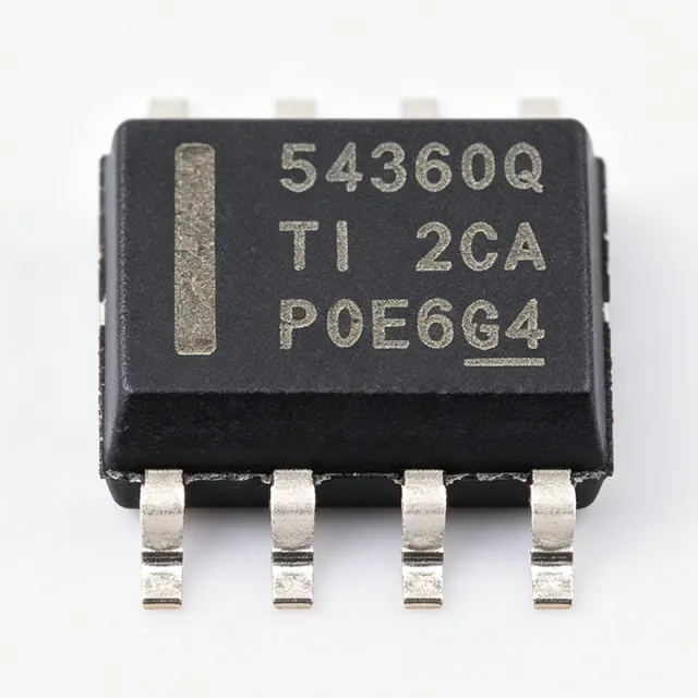
What Is the TPS54360QDDARQ1 and Which Verified Specs Matter Most?
The TPS54360QDDARQ1 is a single-output, wide-input synchronous buck regulator from Texas Instruments built for automotive and industrial point-of-load conversion. Per the verified XAIPART product database, its headline specifications are:
| Parameter | Value (verified) |
|---|---|
| Topology | Buck (Step-Down) |
| Input Voltage Range | 4.5 V to 60 V |
| Output Voltage Range | 0.8 V adjustable upward via resistor divider |
| Maximum Output Current | 3.5 A |
| Number of Outputs | 1 |
| Load Dump Survivability | 65 V per ISO 7637 |
| Control Topology | Current Mode |
| Light-Load Mode | Eco-mode pulse-skip (low ripple) |
| Operating Temperature | -40C to +125C |
| Package | 8-PowerSOIC (DDA, SO-8 PowerPAD, 3.90 mm width) |
| Mounting Type | Surface Mount |
| Qualification | AEC-Q100 (Automotive Q1) |
| Integrated FET | High-side MOSFET integrated |
| RoHS Status | [DATA_NEEDED: RoHS status] |
| Switching Frequency | [DATA_NEEDED: switching frequency] |
The Q1 suffix signals AEC-Q100 qualification, and the -40C to +125C ambient range targets harsh vehicle environments such as underhood and exterior lighting locations. Lifecycle status is active in the database.
How Do You Design In the TPS54360QDDARQ1? A Practical Technical Guide
The TPS54360QDDARQ1 uses peak current-mode control with an integrated 60V power MOSFET, which reduces external component count versus a controller-plus-discrete-FET solution. The internal bootstrap and soft-start functions simplify startup design.
Output voltage setting: The regulated output is adjustable from a 0.8V reference using a resistor divider on the VSENSE pin. Choose the top feedback resistor first, then derive the bottom resistor for your target output of 0.8V or higher.
Inductor selection: At 60V input the converter operates at high switching-step ratios. Ensure the external inductor saturation current exceeds the 3.5A peak current limit. [VERIFY_NEEDED: recommended inductance values per TI datasheet for specific Vout/frequency combinations.]
Thermal design: The exposed PowerPAD beneath the SO-8 package must be soldered to a grounded PCB thermal pad; it provides both the electrical ground connection and the low thermal resistance heat path. Adequate PCB copper area on the PowerPAD is required for full 3.5A operation.
Layout: Follow TI's datasheet layout guidelines and place the input decoupling capacitor very close to the VIN and GND pins to minimize the high-frequency switching loop.
Light-load behavior: Eco-mode pulse-skip operation reduces switching losses when load current drops, keeping efficiency high for always-on nodes; TI describes this mode as low-ripple, so it remains suitable for noise-sensitive analog rails after verification on your board.
Pinout Reference (Verified)
| Pin | Name | Function |
|---|---|---|
| 1 | BOOT | Bootstrap capacitor connection for high-side gate driver |
| 2 | VIN | Input supply, 4.5V to 60V |
| 3 | EN/UVLO | Enable and adjustable undervoltage lockout |
| 4 | SS/TR | Soft-start / tracking control |
| 5 | VSENSE | Feedback voltage sense for output regulation |
| 6 | COMP | Error amplifier output for loop compensation |
| 7 | GND | Ground reference |
| 8 | PH | Phase (switch node) connection to inductor |
| Pad | PowerPAD | Exposed thermal pad, must be soldered to grounded copper for thermal and electrical performance |
For the complete, latest-revision electrical characteristics, download the datasheet from the official TI TPS54360-Q1 product page or view the TPS54360QDDARQ1 product page on XAIPART.
What Are the Drop-in Alternatives and How Does TPS54360QDDARQ1 Compare?
Within the verified alternatives data, two family substitutes exist. Both share the SO-8 PowerPAD (DDA) footprint and pinout, so no PCB rework is needed when substituting within the family.
| Parameter | TPS54360QDDARQ1 | TPS54360BQDDARQ1 | TPS54560QDDARQ1 |
|---|---|---|---|
| Input Voltage Range | 4.5 V to 60 V | 4.5 V to 60 V (same AEC-Q1 family) | 4.5 V to 60 V (same AEC-Q1 family) |
| Max Output Current | 3.5 A | 3.5 A (same die, B-version option) | 5 A |
| Package | SO-8 PowerPAD (DDA) | SO-8 PowerPAD (DDA) | SO-8 PowerPAD (DDA) |
| Qualification | AEC-Q100 | AEC-Q100 | AEC-Q100 |
| Control | Current Mode | Current Mode (family) | Current Mode (family) |
How to choose: The TPS54360BQDDARQ1 is the same 60V 3.5A AEC-Q1 die in a B-version ordering option (per Mouser listing), useful when a B-suffix part number is mandated by a customer drawing. Choose the TPS54560QDDARQ1 when up to 5A output is needed; otherwise the 3.5A TPS54360QDDARQ1 is the cost-effective choice. For non-automotive builds, the commercial-grade TPS54360DDAR is a pin-compatible drop-in of the same die without automotive qualification. Direct pin-compatible cross-brand equivalents in the SO-8 PowerPAD footprint with 60V rating are scarce; most competitor 60V bucks (such as MPS MP4560 family parts) use different pin maps and require PCB re-checks, so verify any cross-brand candidate pin-by-pin against the TPS54360-Q1 pinout before qualification.
Current XAIPART pricing for TPS54360QDDARQ1 as of 2026-09-04: $4.10 at qty 1, $3.70 at qty 10, $3.20 at qty 100, $2.80 at qty 500, and $2.45 at qty 1,000.
What Is the Market Position, Lifecycle, and Supply Situation for TPS54360QDDARQ1?
The XAIPART database lists lifecycle status as active, with 99,999 units in stock, MOQ of 1, and tiered pricing from $4.10 down to $2.45 as of 2026-09-04. This deep stock position supports both prototype buys and production scheduling. [DATA_NEEDED: manufacturer forecasted end-of-life status and allocated-supply outlook beyond database lifecycle flag.]
What Trends Should Buyers Watch for This 60V Automotive Buck Family?
Three trends are directly anchored to verified specs. First, zone-controller and always-connected vehicle architectures keep demanding wide-input battery-direct regulators: the 4.5V to 60V window with 65V ISO 7637 load-dump survivability lets one buck cover 12V cold-crank, 24V buses, and jump-start events without a pre-regulator, consolidating BOMs. Second, standby drain scrutiny favors parts like this one with Eco-mode pulse-skip light-load operation, since body electronics and telematics nodes spend most of their life at light load. Third, heat-density pressure in compact enclosures (DIN-rail modules, telematics dongles) rewards the SO-8 PowerPAD thermal strategy; buyers should confirm their PCB copper area supports full 3.5A operation. When 5A headroom is forecast, plan the migration path to the pin-compatible TPS54560QDDARQ1 now to avoid layout changes later. Watch family pinout compatibility before attempting any cross-brand substitution, since verified cross-brand drop-ins in this footprint are scarce.
Where Should You Apply the TPS54360QDDARQ1 in Real Designs?
Verified application data covers six scenarios: automotive battery-direct power rails (absorbing cold-crank to 4.5V and load dump to 65V), 24V industrial bus point-of-load conversion with Eco-mode standby efficiency, automotive infotainment and cluster supplies generating 5V intermediate rails, motor drive and actuator logic supplies where current-mode control rejects bus droop, body electronics and lighting modules wired directly to battery, and telematics/connectivity modules that must hold regulation through engine crank. In each case the combination of 60V input tolerance, 3.5A output, AEC-Q100 qualification, and -40C to +125C operation is the enabling spec set.
Ready to source? Check live stock and request a quote on the TPS54360QDDARQ1 product page, browse the full DC-DC converter category, or read more in our technical guides library.
Comments
Be the first to comment.
🔐 Please sign in to post a comment.
Don't have an account? Sign up