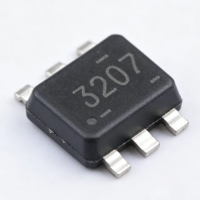
The Texas Instruments TPS563207DRLR is a 3-A synchronous buck (step-down) converter in a 6-pin SOT-563 (DRL) package measuring just 1.6 mm x 1.6 mm. It accepts 4.3 V to 17 V input, produces an adjustable output down to 0.806 V, uses D-CAP2 mode control with Forced CCM (FCCM) operation, and is specified from -40C to +125C junction temperature. The device is RoHS compliant, lifecycle status is active, and it is available from XAIPART with 99,999 units in stock, MOQ 1, at $0.31 per unit at 1,000 pieces (pricing as of 2026-09-04).
This pillar guide consolidates everything a design engineer or buyer needs: verified specifications, a design-in walkthrough with the exact pinout, drop-in alternatives within the TI family, and sourcing guidance.
What Are the Quick Answers About the TPS563207DRLR?
The TPS563207DRLR is a monolithic synchronous buck regulator with integrated high-side and low-side MOSFETs, delivering up to 3 A of continuous output current. Key verified specifications: input voltage range 4.3 V to 17 V, adjustable output from 0.806 V, D-CAP2 control mode, FCCM operation for low light-load ripple, one adjustable positive output, and support for low-ESR ceramic and specialty polymer output capacitors. The 17-V maximum input covers 12-V buses with margin. Availability is strong: XAIPART lists 99,999 units in stock with MOQ 1, priced from $0.62 at qty 1 down to $0.31 at qty 1,000, as of 2026-09-04. Switching frequency is [DATA_NEEDED: switching frequency] and the internal feedback reference voltage is [DATA_NEEDED: feedback reference voltage] in the verified database; consult the TI datasheet for these values before finalizing designs.
How Do You Select and Design In the TPS563207DRLR?
Designing in the TPS563207DRLR is straightforward because internal compensation and internal soft-start reduce external component count to typically an inductor plus input and output capacitors, plus a feedback divider and an enable resistor per the datasheet.
Step 1: Confirm Rail Compatibility
Verify your input rail sits within the 4.3 V to 17 V window. The part accepts 5-V and 12-V intermediate buses directly. Its 0.806-V adjustable output floor covers common 1.0-V, 1.2-V, 1.8-V, and 3.3-V rails via a resistor divider.
Step 2: Understand the Control Mode Choice
D-CAP2 mode control combines a wide-bandwidth error amplifier with an adaptive on-time generator. This enables near-constant frequency operation, fast transient response to load steps with minimal output capacitance, and support for low-ESR output capacitors such as specialty polymer and ultra-low-ESR ceramic types. Fixed-frequency FCCM operation maintains small output ripple even at light loads. If your application prioritizes light-load efficiency over ripple, family members like the TPS563201 (eco-mode/DCM) may fit better; choose the TPS563207 when forced-CCM operation with low light-load ripple is required.
Step 3: Use the Verified Pinout Correctly
Connect the power stage first (VIN pin 4, SW pin 3 to the inductor, GND pin 2), then the control pins: EN (pin 1), FB (pin 5) to the output divider, and BOOT (pin 6) with a bootstrap capacitor to SW for the high-side gate driver. Full electrical characteristics and layout guidelines are in the official datasheet PDF.
Step 4: Set the Output Voltage
The output is set with an external resistor divider from VOUT to the FB pin. Use 1%-tolerance resistors and the datasheet formula VOUT = Vref x (1 + R1/R2). The converter regulates when FB reaches the internal reference; the verified database lists the adjustable output starting at 0.806 V.
Step 5: Manage Thermal Performance
The 1.6-mm x 1.6-mm DRL package dissipates heat mainly through the PCB, so copper area on the ground and switch-node nets determines junction temperature at full 3-A load. The device is specified from -40C to +125C junction temperature; verify your layout meets this at maximum load and ambient. Per the TI datasheet FAQ guidance, check junction temperature at full load before production release.
Step 6: Layout for the SOT-563 Footprint
The tiny footprint suits dense point-of-load layouts such as SSDs, modules, and networking boards. Keep the input capacitor close to VIN and GND, route the SW node compactly, and place the FB divider away from the SW node to protect regulation accuracy.
What Are the Best Alternatives and How Does TPS563207DRLR Compare?
All verified drop-in alternatives come from the same TI family and share the identical 6-pin SOT-563 (DRL) pinout and footprint. Note that the TPS560200DBVR is sometimes compared but is rated for only about 200 mA output in SOT-23-5, so it is not drop-in interchangeable for a 3-A rail.
| Parameter | TPS563207DRLR | TPS563207SDRLR | TPS563201DRLR | TPS563208DRLR | TPS563211DRLR | TPS563212DRLR | TPS56A207DRLR |
|---|---|---|---|---|---|---|---|
| Package | SOT-563 (DRL), 6-pin | SOT-563 (DRL), 6-pin | SOT-563 (DRL), 6-pin | SOT-563 (DRL), 6-pin | SOT-563 (DRL), 6-pin | SOT-563 (DRL), 6-pin | SOT-563 (DRL), 6-pin |
| Input range | 4.3 V - 17 V | 4.3 V - 17 V | Same family, verify in datasheet | Same family | Same family | Same family | Same family |
| Control mode | D-CAP2, FCCM | S-variant of same converter | Eco-mode (DCM) | Different control-mode/feature set; verify FCCM behavior | Same family | Alternate frequency version of TPS563211 | Same family |
| Current rating | 3 A | Same family | Verify vs. requirements | Verify | 3 A | Same family | Higher current (margin upgrades) |
| Key differentiator | FCCM, low light-load ripple | S-variant, differing specified operating characteristics | Higher light-load efficiency | Feature-set variant | Different switching-frequency option | Alternate frequency option | Margin upgrade in same footprint |
Substitution guidance: All listed alternatives share the same pinout and footprint, so footprint-driven substitutions remain possible. Always verify control mode (FCCM vs. eco-mode), current rating, and switching-frequency option against your requirements before substitution, and check the pinout in each datasheet before production. A pin-to-pin cross-brand equivalent in the same SOT-563 package is not well established; converters from Richtek or MPS with similar 3-A ratings typically use different packages or pinouts, so staying within the TPS56x2xx SOT-563 family is the safest path for guaranteed drop-in compatibility.
What Is the Market Position, Lifecycle, and Supply Situation for the TPS563207DRLR?
Lifecycle status is active per the verified database, meaning TI continues to manufacture and support the part, and it is safe for new designs. Supply is healthy: XAIPART lists 99,999 units in stock with MOQ 1, so prototypes and small builds can order a single unit. Pricing as of 2026-09-04: $0.62 at qty 1, $0.56 at qty 10, $0.45 at qty 100, $0.38 at qty 500, and $0.31 at qty 1,000. Authorized distribution also includes DigiKey and Mouser, both showing in-stock availability with same-day shipping options as of 2026-08-29. [DATA_NEEDED: long-term lifecycle forecast/EOL notice status].
What Trends and Buying Considerations Should You Watch?
- Space-constrained point-of-load design continues to shrink. At 1.6 mm x 1.6 mm with integrated FETs, the TPS563207DRLR is among the smallest 3-A synchronous buck solutions, which is why it appears in SSDs, networking port-side layouts, and portable devices.
- FCCM vs. eco-mode is the key family trade-off. FCCM keeps output ripple small for noise-sensitive rails (NAND, PHYs, audio/video), while eco-mode variants in the same footprint favor light-load battery efficiency. Decide this trade-off early because it may pin your part choice.
- Thermal layout matters more as packages shrink. The small DRL package relies on PCB copper for heat dissipation; budget ground pour area at the 3-A full-load point, targeting the -40C to +125C junction spec.
- Cost per amp is competitive. At $0.31/unit at 1,000 pieces (as of 2026-09-04), the part supports cost-sensitive consumer electronics rails (HDMI, SoC, wireless modules) with BOM-minimal external parts.
- Buy with margin. If your rail current may grow, TPS56A207DRLR offers a higher-current family member in the same SOT-563 footprint, simplifying an upgrade without a board respin.
How Should You Apply the TPS563207DRLR in Real Systems?
Verified application scenarios from the product database include networking equipment point-of-load (12-V bus to PHY/MAC/memory rails), SSD and storage power (12-V SATA/NVMe input matching), industrial automation control (PLC I/O with -40C to +125C robustness), FPGA/ASIC auxiliary rails (0.806-V floor covers 1.0-3.3 V banks), consumer electronics power (sub-$0.70 unit cost, low ripple for A/V), and battery-powered portable devices (17-V max input suits 3S-4S lithium stacks). In each case, the combination of 3-A integrated FETs, D-CAP2 fast transients, FCCM low ripple, and the minimal external BOM (inductor plus input/output capacitors) drives the selection.
Example design solution: Generate a 3.3-V, 3-A rail from a 12-V input for a networking switch port card. Use the TPS563207DRLR with a power inductor per the datasheet equations, low-ESR ceramic input and output capacitors (D-CAP2 mode supports ultra-low-ESR ceramics), and a 1%-tolerance feedback divider solving VOUT = Vref x (1 + R1/R2). Verify junction temperature on the PCB at 3 A and confirm the 12-V input stays within the 4.3-17 V window including transients. For exact inductor and capacitor values, apply the datasheet application equations.
Ready to source? Visit the TPS563207DRLR product page on XAIPART, browse our DC-DC converters category, or read more in our technical guides library.
Comments
Be the first to comment.
🔐 Please sign in to post a comment.
Don't have an account? Sign up