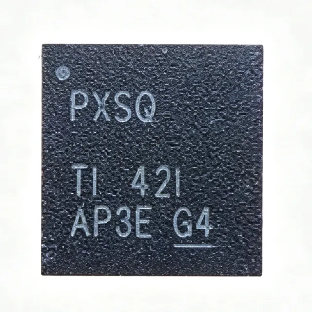
What Is the TPS7A4700RGWR and Why Should Engineers Choose It?
The Texas Instruments TPS7A4700RGWR is a positive, ultralow-noise low-dropout (LDO) linear regulator that sources up to 1 A from a 3 V to 36 V input, delivering an output programmable from 1.4 V to 20.5 V in a 5x5 mm 20-pin VQFN (RGW) package with an exposed thermal pad. Its headline specification is 4.17 µVRMS output noise (20 Hz to 100 kHz) combined with high power supply rejection ratio (PSRR), making it a premier post-regulator for noise-sensitive analog rails. Unlike conventional adjustable LDOs, the ANY-OUT technique programs the output voltage through PCB layout connections to sense-pin combos — no external feedback resistors or feed-forward capacitors — which removes divider thermal noise from the output and shortens the sense path. The part is active in lifecycle status, RoHS compliant, rated MSL 2 (260 °C, 1 year), and widely stocked: 99,999 units are available on XAIPART as of 2026-08-30, with pricing from $6.2727 at 1 unit down to $3.6591 at 1,000 units. Note that this variant has no enable pin; the pin-compatible TPS7A4701 adds one.
In the power-management hierarchy, an LDO typically follows a switching converter or battery to generate a clean analog rail for loads such as op-amps, ADCs, and PLL/VCO blocks. The TPS7A4700RGWR's bipolar architecture with a precision bandgap reference delivers the high PSRR needed to suppress switching-converter ripple before it reaches those sensitive loads. With a 36 V maximum input, it also provides generous surge headroom above nominal 24 V industrial buses — a capability few ultralow-noise LDOs offer.
How Do You Select and Design In the TPS7A4700RGWR?
Start with four boundary checks against the verified specs:
| Parameter | Verified Value |
|---|---|
| Input voltage range | 3 V to 36 V |
| Output voltage range | 1.4 V to 20.5 V (ANY-OUT via PCB layout) |
| Maximum output current | 1 A |
| Output noise | 4.17 µVRMS (20 Hz to 100 kHz) |
| Package | VQFN-20 (RGW), 5x5 mm, exposed pad |
| Mounting / MSL | Surface mount / MSL 2 (260 °C, 1 year) |
Step 1 — Validate headroom. Confirm your input rail sits between 3 V and 36 V and that the input-to-output differential stays within the dropout capability of the device at your load current. For dropout voltage at 1 A and quiescent current figures, consult the official TI datasheet at https://www.ti.com/lit/gpn/TPS7A47. [VERIFY_NEEDED: dropout voltage and quiescent current values]
Step 2 — Program the output with ANY-OUT. This is the signature design step. Instead of an external resistor divider, you connect (or leave floating) a set of ANY-OUT sense pins on the PCB to select the output voltage from 1.4 V to 20.5 V. Use the ANY-OUT programming table in the TI datasheet to map your target rail to the correct pin connections. This eliminates resistor thermal noise from the output node and removes two to three BOM positions per rail.
Step 3 — Manage the noise-reduction/soft-start pin. Pin 4 (NR/SS) accepts a noise reduction and soft-start capacitor. Sizing this capacitor shapes output startup and further lowers the noise floor; see the datasheet application section for recommended values.
Step 4 — Thermal design. The exposed thermal pad must connect to GND with adequate copper pour underneath for thermal relief. For θJA and the operating temperature range, refer to the datasheet thermal tables. [VERIFY_NEEDED: theta JA and operating temperature range]
Step 5 — Decide between TPS7A4700 and TPS7A4701. The TPS7A4700RGWR has no enable pin (pin 3 is EN/NC on this variant). If your power sequence requires rail enable control, choose the TPS7A4701RGWR, which adds an active-high enable in the identical VQFN-20 footprint — both are otherwise drop-in compatible within the family.
Step 6 — Layout for low noise. Keep input and output capacitors (typical application uses 10 µF ceramic input/output capacitors per the verified application guidance) close to their pins, route the ANY-OUT sense connections per the programming table, and keep the sense path short — the absence of an external divider is precisely what preserves the 4.17 µVRMS floor.
Which Key Pins Matter Most on the TPS7A4700RGWR?
The critical pins for bring-up are the input supply pins, ground, output, noise-reduction/soft-start, the ANY-OUT sense combo pins, and the exposed thermal pad. Pin 3 functions as EN/NC on this variant (no enable function on the TPS7A4700). The complete 20-pin table, including exact per-pin ANY-OUT voltage mappings, lives on the TPS7A4700RGWR product page and in the TI datasheet.
What Are the Best Drop-In Alternatives to the TPS7A4700RGWR?
Within the TI family, substitution is straightforward; cross-brand swaps require PCB rework.
| Parameter | TPS7A4700RGWR | TPS7A4701RGWR | TPS7A4700QRGWRQ1 | LT3045EDD | TPS7A3301RGWR |
|---|---|---|---|---|---|
| Polarity / Type | Positive LDO | Positive LDO | Positive LDO | Positive LDO | Negative LDO |
| Input range | 3–36 V | 3–36 V | 3–36 V | Up to 5.5 V | -36 V to -1.2 V (output) |
| Output current | 1 A | 1 A | 1 A | 500 mA | [DATA_NEEDED: output current] |
| Output noise | 4.17 µVRMS | 4.17 µVRMS | 4.17 µVRMS | 0.8 µVRMS | [DATA_NEEDED: noise] |
| Package | VQFN-20 (RGW) | VQFN-20 (RGW) | VQFN-20 (RGW) | Different package | Same footprint |
| Drop-in? | — | Yes (adds enable) | Yes (automotive) | No — PCB rework | Complementary, not substitute |
Recommendations: For power sequencing, choose TPS7A4701RGWR and tie EN high if unused. For AEC-Q100 automotive designs, choose TPS7A4700QRGWRQ1 or TPS7A4701QRGWRQ1 — identical 36 V/1 A/4.17 µVRMS performance with automotive-grade screening. The TPS7A4700RGWT is the same die in tape-and-reel packaging. Cross-brand, the Analog Devices LT3045 offers even lower noise (0.8 µVRMS) at 500 mA but only accepts up to 5.5 V input and requires a different footprint. The TPS7A3301RGWR is a negative-polarity LDO in the same footprint — complementary for split-rail designs, not a substitute.
Where Does the TPS7A4700RGWR Fit in Real Applications?
Five verified application scenarios showcase its strengths:
RF transceiver PLL/VCO rails. Phase noise depends directly on supply cleanliness. Place the TPS7A4700RGWR as a post-regulator after a DC-DC converter to suppress switching ripple before it reaches the oscillator tuning port; the 36 V input also supports RF modules fed from higher-voltage industrial supplies. Use 10 µF ceramic input/output capacitors with short sense routing.
Precision test and measurement instrumentation. Bench instruments need microvolt-level rail purity. The 4.17 µVRMS noise, bandgap reference, and ANY-OUT topology (no divider thermal noise) support ADC/DAC reference supplies and op-amp rails; 1 A capacity covers multiple signal-chain blocks from one regulator.
Audio DAC and headphone amplifier supply. The 4.17 µVRMS noise over 20 Hz–100 kHz sits far below the audible threshold, and high PSRR rejects upstream switcher ripple that would otherwise surface as audible artifacts.
Industrial 24V bus sensor conditioning. The 36 V rating leaves surge headroom above nominal 24 V buses; post-regulate after an efficient buck stage for clean analog rails, with ANY-OUT matching rail voltages to sensor requirements without extra resistors.
Medical diagnostics and automotive analog rails. Medical biosignal amplifiers benefit from the low noise floor and 1 A multi-channel capability; for automotive infotainment and ADAS modules, the AEC-Q100 TPS7A4700QRGWRQ1 delivers identical performance for 12 V-battery transient environments.
How Do You Build a Clean 5V Analog Rail from a 24V Industrial Bus? (Design Example)
Problem: A factory sensor front end runs from a nominal 24 V industrial bus and needs a low-noise 5 V analog rail for conditioning amplifiers and an ADC. Switching ripple from the first conversion stage must not reach the analog domain.
Approach: Use a DC-DC buck to step 24 V down efficiently to ~6 V, then post-regulate with the TPS7A4700RGWR programmed to 5.0 V via ANY-OUT PCB connections. This architecture exploits the LDO's high PSRR to reject switching residue while the 36 V input rating covers bus transients.
Components: 1x TPS7A4700RGWR (main LDO), 1x buck pre-regulator (any suitable switching converter), 10 µF ceramic input capacitor, 10 µF ceramic output capacitor, NR/SS capacitor per datasheet recommendation.
Schematic description: 24 V bus → buck converter → 6 V intermediate rail → TPS7A4700RGWR IN (pins 1–2) → 5.0 V OUT (pins 7–8) → analog load. NR/SS (pin 4) to ground via soft-start capacitor; ANY-OUT sense combos (pin 6 group) strapped per the datasheet table for 5.0 V; exposed thermal pad soldered to a grounded copper pour.
Calculations: Load budget — with 1 A maximum output current, the rail supports the full analog front end with margin. Thermal check — dissipation is (V_IN − V_OUT) × I_LOAD = (6 V − 5 V) × I_LOAD; at 500 mA that is 0.5 W, manageable with the exposed-pad pour; verify against the datasheet θJA. [VERIFY_NEEDED: theta JA value for exact rise calculation]
Results: A single-chip analog rail with 4.17 µVRMS noise, no feedback resistors in the BOM, and surge headroom up to 36 V input — cleaner and simpler than a resistor-adjustable alternative.
What Is the Market Position, Lifecycle, and Supply Situation for the TPS7A4700RGWR?
The TPS7A4700RGWR carries an active lifecycle status, per the verified database. Supply is healthy: XAIPART lists 99,999 units in stock with MOQ 1 as of 2026-08-30, and the part is also stocked at DigiKey and Mouser as of 2026-08-29. Pricing at XAIPART, as of 2026-08-30: $6.2727 (qty 1), $4.5303 (qty 10+), $4.0076 (qty 100+), $3.8333 (qty 500+), and $3.6591 (qty 1,000+). Long-term lifecycle forecasts and end-of-life risk assessments: [DATA_NEEDED: lifecycle forecast data].
What Should Buyers Watch Next for Ultralow-Noise LDO Sourcing?
Anchor your sourcing decisions to the verified spec envelope: the 3–36 V input range and 4.17 µVRMS noise are the reasons this part wins designs that lower-voltage ultra-low-noise LDOs like the LT3045 (5.5 V max input, 500 mA) cannot serve. Watch three things. First, variant selection: if a design revision needs sequencing, moving to the pin-compatible TPS7A4701RGWR is a zero-rework change. Second, automotive programs should standardize on the TPS7A4700QRGWRQ1/TPS7A4701QRGWRQ1 AEC-Q100 variants early to avoid requalification. Third, volume pricing scales meaningfully — moving from single-unit buys to 1,000-piece lots cuts unit cost from $6.2727 to $3.6591 (as of 2026-08-30), roughly a 42% reduction. Because no verified cross-brand pin-to-pin equivalent exists in the same VQFN-20 footprint, single-sourcing risk concentrates on the TI family; keep the TPS7A4700RGWT (same die, tape-and-reel) and the automotive variants in your approved alternate list. Check current XAIPART stock and pricing before committing a BOM.
Comments
Be the first to comment.
🔐 Please sign in to post a comment.
Don't have an account? Sign up