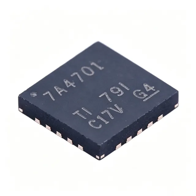
The Texas Instruments TPS7A4701RGWR is an ultra-low-noise, high-PSRR LDO linear regulator that delivers up to 1A of output current with just 4.17 uVrms of output noise (20 Hz to 100 kHz) and 72 dB of PSRR at 1 kHz. It accepts input voltages from 3V to 35V, produces an adjustable output from 1.4V to 34V, and drops only 200 mV at full 1A load. The device comes in a compact 5x5 mm VQFN-20 (RGW) package with a 31.4 C/W thermal resistance, operates from -40C to +125C, and is RoHS compliant. As of 2026-09-02, TPS7A4701RGWR is in stock on XAIPART with 99999 units available, a minimum order quantity of 1, and a unit price of $3.2467. The lifecycle status is active, making it a safe choice for new designs. This guide covers how to select, design in, and deploy this regulator, compares drop-in alternatives, and explains what buyers should watch in this product segment.
What Are the Quick Answers About the TPS7A4701RGWR?
The TPS7A4701RGWR answers the most common noise-critical power supply questions in a single device. It is a 1A adjustable LDO from Texas Instruments with 4.17 uVrms output noise over 20 Hz to 100 kHz and 72 dB PSRR at 1 kHz, suited for audio DACs, RF PLL/VCO rails, precision ADC reference buffering, and test instrumentation. Its wide 3V to 35V input range supports industrial 24V bus systems with adequate headroom, while its active-high enable pin supports sequential power-up in multi-rail systems. It includes thermal shutdown protection and a 6.4 mA quiescent current. Supply is strong: 99999 units in stock as of 2026-09-02 at $3.2467 each with MOQ 1, and the part is active in TI's lifecycle. For automotive programs, the AEC-Q100 qualified TPS7A4701RGWR-Q1 variant shares the same package and pinout.
How Do You Select and Design In the TPS7A4701RGWR?
Step 1: Confirm Your Input and Output Requirements
Verify that your input rail falls within the 3V to 35V input range and your target output falls within the 1.4V to 34V adjustable range. The adjustable version sets the output using two external resistors with the formula VOUT = 1.4V * (1 + R1/R2), per TI datasheet SBOS708B. For example, to generate 5V from a 12V rail, choose resistor values that satisfy R1/R2 = (5/1.4) - 1, approximately 2.571. [DATA_NEEDED: recommended resistor value ranges from datasheet]
Step 2: Budget Your Thermal Dissipation
Thermal design is the most critical step. At VIN = 12V, VOUT = 5V, and a 1A load, the device dissipates approximately 7W. With a theta_JA of 31.4 C/W, junction temperature would rise roughly 220C above ambient — well beyond safe operation. TI guidance in the verified FAQ states that a heatsink or a substantial copper pour of at least 1 square inch is required for reliable operation above 2-3W of dissipation. Size your copper area or heatsink so the junction stays within the -40C to +125C operating range under worst-case load and ambient conditions. Where possible, increase headroom efficiency by lowering VIN-VOUT differential; the 200 mV dropout at 1A allows operation close to the output voltage, dramatically reducing dissipation.
Step 3: Use the Enable Pin for Power Sequencing
The TPS7A4701 includes an active-high enable pin (Pin 6, EN) that supports sequential power-up in multi-rail systems — essential for processors requiring specific rail sequencing. Drive EN from a supervisor or another rail's power-good signal to enforce order.
Step 4: Leverage the Noise Reduction / Soft-Start Pin
Pin 11 (NR/SS) provides noise reduction and soft-start functionality. Use the recommended capacitor on this pin per the datasheet to further reduce output noise below the already excellent 4.17 uVrms figure and to control startup behavior. [DATA_NEEDED: recommended NR/SS capacitance values]
Step 5: Maximize the Thermal Pad
The VQFN-20 (RGW) 5x5 mm package uses an exposed thermal pad. Pins 13 through 20 are all GND pins, and the pad itself must be soldered to a solid ground plane. The eight GND pins plus the exposed pad minimize ground impedance and carry heat into the PCB, which is essential given the 31.4 C/W thermal resistance.
What Does the Pinout Look Like and How Should You Connect It?
The 20 pins are organized functionally: output, input, ground, and control. Pins 1-4 are parallel OUT connections for the regulated output, Pins 7-10 are parallel IN connections for the input supply, Pin 6 is the active-high EN, Pin 11 is NR/SS, Pin 12 is FB (feedback), and the remaining pins are GND. Place the input and output capacitors close to their respective pins and route the FB divider away from noisy switching nodes. The key functional pins are summarized in the pinout_data structured block on this page, and the complete table lives on the TPS7A4701RGWR product page.
What Are the Main Applications for This LDO?
The verified application set includes: high-end audio DAC power supplies (clean 5V rails with 4.17 uVrms noise), RF transceiver PLL/VCO power, precision ADC reference buffering, test and measurement instrumentation, industrial 24V bus regulation down to low-noise sensor rails, and portable medical devices. In each case, the combination of 72 dB PSRR at 1 kHz and ultra-low output noise is the deciding factor — an upstream switching converter's ripple is rejected before it reaches the sensitive load.
What Are the Drop-In Alternatives to the TPS7A4701RGWR?
Two verified alternatives exist within the TPS7A4701 family. The TPS7A4701RGWR-Q1 is the AEC-Q100 automotive-qualified variant sharing the same die, VQFN-20 (RGW) package, and pinout. The TPS7A4701RGWT is the same die in tape-and-reel packaging, ideal for high-volume automated assembly. The TPS7A4700 (same package, identical 4.17 uVrms noise and 72 dB PSRR specs) differs by omitting the enable pin, so it is a drop-in replacement only when power sequencing is not required.
| Parameter | TPS7A4701RGWR |
|---|---|
| Output Type | Adjustable |
| Output Voltage Range | 1.4 V to 34 V |
| Maximum Output Current | 1 A |
| Input Voltage Range | 3 V to 35 V |
| Dropout Voltage | 200 mV at 1 A |
| Output Noise | 4.17 uVrms (20 Hz to 100 kHz) |
| PSRR | 72 dB at 1 kHz |
| Quiescent Current | 6.4 mA |
| Thermal Resistance | 31.4 C/W |
| Operating Temperature | -40C to +125C |
| Package | VQFN-20 (RGW) 5x5 mm |
| Enable Pin | Yes (active-high) |
| AEC-Q100 Qualified | No (TPS7A4701RGWR-Q1 variant is qualified) |
| Price (as of 2026-09-02) | $3.2467 (qty >= 1) |
Where Does the TPS7A4701RGWR Stand in the Market and Supply Chain?
The TPS7A4701RGWR carries an active lifecycle status, meaning Texas Instruments continues to produce and support it and recommends it for new designs. On XAIPART, supply depth is excellent: 99999 units in stock as of 2026-09-02, with a single-unit MOQ at $3.2467 per unit, which removes minimum-order barriers for prototyping. [DATA_NEEDED: long-term lifecycle forecast, competitor market share, and lead-time data]
What Should Buyers Watch Going Forward?
Three considerations anchored to verified specs should guide purchasing and design decisions. First, thermal budget dominates feasibility: with 31.4 C/W theta_JA, applications above roughly 2-3W dissipation need PCB copper or heatsinking, so evaluate your VIN-VOUT differential early — the 200 mV dropout at 1A is your efficiency ally. Second, if your program is automotive, specify the TPS7A4701RGWR-Q1 from the start rather than redesigning later; it shares the same package and pinout. Third, the active-high enable pin differentiates this part from the enable-less TPS7A4700, so confirm sequencing requirements before finalizing a BOM. With 99999 units in stock and active lifecycle status as of 2026-09-02, supply risk is currently low, but noise-critical analog designers should keep this family qualified across second sources of upstream DC/DC stages to fully exploit the 72 dB PSRR.
Comments
Be the first to comment.
🔐 Please sign in to post a comment.
Don't have an account? Sign up