FPGA ও CPLD
পণ্য (7,100+)

EPM9560WI208-20 - 560-Cell CPLD, 23.6ns, CQFP-208 | Intel / Altera
The Intel / Altera EPM9560WI208-20 is a high-density 560-cell Complex Programmable Logic Device (CPLD) from the MAX 9000 family, housed in a 208-pin Ceramic Quad Flat Pack (CQFP208) package with gull-wing leads. It provides 23.6ns pin-to-pin logic delay, 560 macrocells, 16 logic array blocks, and up to 212 user I/O pins for complex glue-logic, bus-interface, and state-machine designs. The device is built on a 0.35-micron CMOS EEPROM process and is rated for industrial temperature operation. A Complex Programmable Logic Device (CPLD) is a non-volatile programmable logic IC that combines multiple PAL-like macrocell blocks with a programmable interconnect matrix. In the broader taxonomy it sits under programmable logic -> PLD -> CPLD -> MAX 9000 series -> high-density glue logic. CPLDs are commonly deployed as deterministic, low-latency controllers alongside microprocessors, FPGAs, and ASICs, providing boot configuration, address decoding, bus arbitration, and custom I/O expansion with predictable timing and instant-on behavior from on-chip EEPROM. Key features of the EPM9560WI208-20 include 560 macrocells, 16 logic array blocks (LABs), 212 maximum user I/O pins, 23.6ns worst-case pin-to-pin propagation delay (tPD), a JTAG-based IEEE 1149.1 boundary-scan interface, and in-system programmability via JTAG. The internal EEPROM configuration cells allow instant-on operation at power-up without external boot memory, and the device is supported by the Altera MAX+PLUS II and Quartus design tools. The MAX 9000 architecture splits the device into LABs connected by a programmable interconnect array (PIA). Each macrocell contains a programmable-AND/OR array, a flip-flop, and product-term steering, which gives the part deterministic 23.6ns timing across all paths. The 560-cell capacity places this device in the upper tier of the MAX 9000 family, suitable for designs that exceed the density of the MAX 7000 family but do not require an FPGA. Typical applications include military and aerospace avionics, industrial process control, telecommunication line cards, and legacy bus-bridge designs. The ceramic CQFP-208 package is preferred in harsh-environment and high-reliability systems where plastic packages are not acceptable, including down-hole, military, and aerospace programs. When designing with the EPM9560WI208-20, note that the -20 speed grade reflects 23.6ns tPD; faster -15 and -10 grades are available in the same MAX 9000 family for tighter timing budgets. Because this part is in the Ceramic QFP package with gull-wing leads, PCB layout must accommodate the larger pad geometry and inspect for lead coplanarity during assembly. This page synthesizes distributor pricing, drop-in same-family alternatives, application guidance, and comparison data not aggregated in a single location on the Altera / Intel datasheet.

GAL22V10D-15LPNI - 15ns 10-Macrocell E2CMOS PLD DIP-24 | Lattice
The Lattice Semiconductor GAL22V10D-15LPNI is a high-performance, electrically erasable CMOS Programmable Logic Device (PLD) in the industry-standard 22V10 architecture, packaged in a 24-pin PDIP (300-mil, through-hole DIP). It features 10 Output Logic Macrocells (OLMCs), a 15 ns maximum propagation delay, and an internal timing margin equivalent to roughly 83.3 MHz f_max, making it the highest-performance member of the GAL22V10 family. A PLD (Programmable Logic Device) is a digital integrated circuit whose logic function and interconnects are defined by the user after manufacture. Within the IC taxonomy, PLDs sit between fixed-function logic gates and full FPGAs: a PLD implements combinational and registered logic via a programmable AND/OR array with dedicated output macrocells, whereas an FPGA uses distributed look-up tables, block RAM and soft cores. The "22V10" naming convention means 22 inputs (12 dedicated + 10 feedback) feeding 10 macrocells with variable drive polarity — this generic footprint is supported across multiple vendors, including Lattice, Atmel/Microchip and AMD, giving designers drop-in second sources. Key features of the GAL22V10D-15LPNI include 10 ns / 15 ns propagation delay grades, electrically erasable (E2CMOS) technology allowing 100+ reprogram cycles, in-system programmable architecture, a built-in security bit to lock the pattern, and low CMOS standby current with TTL-compatible I/O. The device is functionally and parametric compatible with standard bipolar and CMOS 22V10 devices, including the classic PAL22V10. The GAL22V10D combines a high-performance CMOS process with Electrically Erasable (E2) floating gate technology. The 10 OLMCs are individually configurable as registered, combinatorial, or I/O with selectable output polarity, and feedback paths allow buried state machines. Unlike UV-erasable EPROM-based 22V10s, the E2CMOS cell can be erased electrically in-circuit, which simplifies prototyping and field upgrades. Typical applications include address decoding and glue logic for microprocessor systems, state-machine and sequencer controllers, bus arbitration logic, peripheral interface adapters, and industrial control replacements of legacy bipolar PALs. Through-hole PDIP packaging suits legacy boards, test fixtures, and aerospace/industrial designs where DIP is preferred over surface mount. When designing, remember the GAL22V10D-15LPNI requires a single 5 V supply (VCC = 4.75 V to 5.25 V) and the JEDEC-standard 22V10 fuse map. Use a Lattice-approved programmer (e.g., ispGAL22V10-compatible) to load the pattern; the security bit, once programmed, prevents readback of the device. This page synthesizes distributor stock data, parametric alternatives, and practical design guidance not aggregated on any single manufacturer or distributor page, giving engineers a single reference for sourcing and second-sourcing the GAL22V10D-15LPNI.
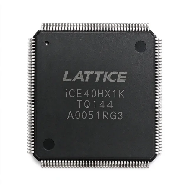
ICE40HX4K-TQ144 - 3520-LUT 1.2V FPGA | Lattice Semiconductor
The Lattice Semiconductor ICE40HX4K-TQ144 is an ultra-low-power HX-series field-programmable gate array (FPGA) with 3,520 logic cells, 107 I/Os, 81,920 bits of configuration memory, and a 144-pin TQFP package. It operates from a 1.2 V core supply according to the supplied distributor data. The device targets compact, low-power programmable logic systems where FPGA flexibility is needed without the power and board complexity of a larger high-performance FPGA. A field-programmable gate array is a configurable digital semiconductor that contains programmable logic blocks, routing resources, input/output blocks, and configuration memory. In the hierarchy, an FPGA is a programmable logic device, a digital IC, and a semiconductor. Unlike a fixed-function microcontroller or application-specific integrated circuit, an FPGA can be programmed after manufacture to implement parallel data paths, control logic, serial interfaces, and hardware signal processing. The ICE40HX4K provides 3,520 logic cells and 81,920 bits of configuration memory, as identified by DigiKey and Mouser search results. Its 107 I/Os provide substantial connectivity for external memory, sensors, communications, control signals, and general-purpose digital interfaces. The HX family is positioned by Lattice as a low-power, high-performance FPGA family, making the part suitable for embedded control, communication, instrumentation, and education platforms where low static power and fast programmable logic are important. The 144-pin TQFP package exposes the FPGA in a conventional surface-mount form factor suitable for automated assembly and multilayer PCB designs. The verified source snippets identify the package as 144-pin TQFP or 144-LQFP terminology; designers should confirm the exact mechanical drawing and pin names against the manufacturer datasheet before releasing a PCB footprint. The supplied data does not specify speed grade, temperature range, power consumption, pin names, memory architecture beyond configuration capacity, or I/O voltage limits. Typical uses include custom interface controllers, low-power sensor aggregation, digital signal conditioning, communications adapters, test fixtures, and FPGA-based education or prototyping boards. For a new design, use the manufacturer’s configuration toolchain and verify pin assignments, supported I/O standards, clocking resources, power rails, decoupling requirements, and programming interface compatibility. Because the supplied evidence confirms the family and capacity but not a complete electrical characterization, unsupported values should not be inferred from generic iCE40 family claims.

ISPLSI - Lattice In-System Programmable Logic Family | CPLD
The Lattice Semiconductor ISPLSI family is a series of high-density, in-system programmable CMOS Complex Programmable Logic Devices (CPLDs) introduced in the early 1990s. The flagship ispLSI 1016 device delivers 2000 PLD gates with 96 registers, 32 universal I/O pins, 4 dedicated inputs, and 3 dedicated clock inputs in a 44-pin package. The family spans multiple sub-series including ispLSI 1000, 2000, 2000E, 2000VE, 3000, 5000V, 8000, and 8000V with gate counts from 1K to 45K and macrocell counts from 32 to 480. A CPLD (Complex Programmable Logic Device) is a type of programmable logic that combines multiple PAL/GAL-like logic blocks on a single chip with a programmable interconnect network. In the broader taxonomy, CPLDs sit alongside FPGAs in the programmable logic category, but use non-volatile EEPROM or flash configuration memory and a deterministic AND-OR logic fabric. Unlike SRAM-based FPGAs, most ispLSI devices retain their configuration without external boot memory, enabling instant-on operation - an important advantage for glue logic, bus interfacing, and power-up deterministic state machine applications. The ispLSI family pioneered 5V in-system programmability (ISP) via a 4-wire JTAG-like interface, allowing devices to be re-programmed on a populated PCB without removing the chip. This eliminated the expensive UV-erase window and programmer sockets required by earlier EPLDs. The Global Routing Pool (GRP) provides complete, deterministic 100% connectivity between all logic blocks and I/O pins with predictable timing - critical for replacing discrete 74-series glue logic in industrial and telecom designs. The ispLSI 2000E sub-family extends the architecture to 32 to 128 macrocells with 1K to 4K gates, while the ispLSI 5000V series scales to 256 macrocells with 12K gates. The ispLSI 8000V reaches 480 macrocells and 45K gates. All members share the same Lattice development flow using ispLEVER or ispDesignEXPERT software. Typical applications include peripheral bus interfacing, address decoding, state-machine replacement of discrete logic, and TTL/CMOS logic consolidation. When designing with ispLSI devices, ensure the JTAG ISP pins (TMS, TCK, TDI, TDO) are accessible for in-system programming. Use Lattice's recommended decoupling (typically 0.1uF per VCC pin) and follow the GRP routing guidelines for predictable timing. Most ispLSI devices are now classified as mature or discontinued by Lattice, so designers should evaluate ispMACH 4000 or MachXO2/XO3 as modern replacements for new designs.

ISPLSI 1032-60LT - 128-Macrocell 5V CPLD, 60MHz, TQFP-100 | Lattice
The Lattice Semiconductor ISPLSI 1032-60LT is a high-density in-system programmable Complex Programmable Logic Device (CPLD) from the ispLSI 1000 family, delivering 6000 PLD gates, 128 macrocells, and 192 registers in a 100-pin TQFP surface-mount package. It operates from a single 4.75 V to 5.25 V supply and provides a maximum propagation delay of 20 ns (60 MHz fMAX). According to the Lattice ispLSI 1032 datasheet, the device integrates 64 universal I/O pins, eight dedicated input pins, four dedicated clock input pins, and a Global Routing Pool (GRP) that distributes signals across the chip with predictable, fixed delay. What is a CPLD? A Complex Programmable Logic Device is a non-volatile programmable logic IC that sits between simple SPLDs/PLAs and large FPGAs in the programmable-logic taxonomy (CPLD -> PLD -> programmable logic -> digital semiconductor). It uses a small-block, sum-of-products architecture with macrocells, making it ideal for implementing wide combinational and registered logic, glue logic, bus decoding, state machines, and address decoding. Unlike SRAM FPGAs, the ispLSI 1032 is non-volatile and in-system programmable via a standard 5-pin JTAG chain, so designs can be updated on production hardware without removing the device. Key features of the ISPLSI 1032-60LT include 32 logic elements (each containing 16 macrocells with associated I/O), 6000 gates of usable logic, 4 dedicated clock inputs feeding four global clock buffers, asynchronous clear and preset per register, JTAG/IEEE 1149.1 boundary-scan test support, and 5 V CMOS I/O with TTL-compatible thresholds. The GRP provides a deterministic, fixed interconnect delay regardless of placement, simplifying timing closure for registered and combinatorial logic. Typical applications include wide address decoding, bus interface glue logic, state-machine controllers, peripheral interface latching, fast counters, frequency and pulse-width measurement, and any design requiring non-volatile, deterministic-timing 5 V glue logic in industrial control, telecom backplane, and embedded processor bus systems. When designing with this device, ensure the 5 V supply is within the 4.75 V to 5.25 V range and that all I/O banks are referenced to a single 5 V rail. Decouple VCC with 0.1 uF and 10 uF capacitors close to the pins. Note that Lattice's own ispMACH 4000V is the recommended modern replacement family for new designs. This page synthesizes distributor pricing, drop-in alternatives, and practical design notes not found in the manufacturer datasheet alone.

ISPLSI1016E-125LT44 - 2K Gates, 64 Macrocells, 125 MHz CPLD | Lattice
The Lattice Semiconductor ISPLSI1016E-125LT44 is a 5 V in-system programmable high-density Complex Programmable Logic Device (CPLD) from the ispLSI 1000E family, delivering 2K usable gates, 64 macrocells, and 96 registers in a 44-pin TQFP (LT44) package. It achieves a pin-to-pin propagation delay (tPD) of 7.5 ns and a maximum operating frequency (fMAX) of 125 MHz, making it suitable for high-speed glue logic and bus-interface bridging in industrial and legacy embedded systems. A CPLD (Complex Programmable Logic Device) is a non-volatile programmable logic device that combines multiple PAL-like macrocell arrays with a central interconnect fabric. CPLDs sit alongside FPGAs in the programmable logic hierarchy, but are distinguished by their deterministic timing, instant-on non-volatile configuration (typically E2CMOS), and lower logic density. The ISPLSI 1000E family belongs to Lattice's first-generation ispMACH-era devices, designed for fast I/O decoding, state-machine replacement, and peripheral interfacing in 5 V systems. Key features of the ISPLSI1016E-125LT44 include 32 universal I/O pins, four dedicated input pins, three dedicated clock input pins, and one global output-enable input routed through a Global Routing Pool (GRP) that provides complete interconnectivity between all logic elements. The device supports 5 V in-system programmability (ISP) via IEEE 1149.1 boundary-scan, enabling firmware upgrades without removing the part from the board. Programmable interconnect and macrocell registers allow designers to replace multiple discrete TTL/CMOS packages with a single non-volatile device. The ispLSI 1016E architecture partitions logic into four Generic Logic Blocks (GLBs), each containing 16 macrocells, a 32-bit product-term array, and dedicated clock/reset/preset control. The GRP delivers 100% connectivity between GLBs and I/O cells with predictable, fixed delays that simplify static timing closure. An on-chip diagnostic TAP allows read-back of programmed state for in-system verification, a feature rare among 5 V CPLDs of this generation. Typical applications include industrial control glue logic, ISA/PCI bus address decoding, peripheral interfacing (UART, FIFO, bus controllers), 5 V legacy system upgrades, and state-machine replacement on 3.3 V-5 V mixed boards. Its 5 V tolerance and industrial temperature grade make it a long-life component for factory automation, instrumentation, and telecom backplane designs where newer 3.3 V-only CPLDs cannot be used directly. When designing with this part, note that the LT44 (TQFP-44) footprint differs from the 44-pin PLCC variant (LJ44). Verify pinout compatibility before PCB rework. Decoupling caps (0.1 uF plus 10 uF bulk) should be placed within 5 mm of each VCC pin, and unused I/O pins must be configured as outputs with defined logic levels to minimize quiescent current. This page synthesizes distributor pricing, drop-in alternatives, and practical design notes not found in the manufacturer datasheet alone, helping engineers source and integrate legacy ispLSI parts confidently.

LC4032B-5T44C - 32-Macrocell 400MHz CPLD | Lattice
The Lattice Semiconductor LC4032B-5T44C is a 3.3V, 2.5V, or 1.8V in-system-programmable SuperFAST high-density PLD with 32 macrocells, a maximum operating frequency of 400MHz, and a propagation delay of 2.5ns. It is supplied in a 48-pin TQFP package, making it suitable for compact systems that require reconfigurable glue logic, interface control, clock distribution, and protocol bridging. A complex programmable logic device, or CPLD, is a programmable logic device that combines nonvolatile configuration storage with a structured array of macrocells. In the hierarchy of programmable logic devices, a CPLD sits above simple programmable logic arrays and provides deterministic timing, repeated in-system programming, and logic capacity suitable for consolidating multiple small fixed-logic functions. The LC4032B family supports 32 macrocells and up to 80 product terms per output, according to the supplied manufacturer-family search result. The principal performance features are a 400MHz maximum operating frequency, 2.5ns propagation delay, support for as many as four global clock pins, and programmable clock-polarity control. The device can operate with 3.3V, 2.5V, or 1.8V supply rails, allowing integration into systems with mixed voltage requirements. Its in-system-programmable architecture supports configuration updates without removing the device from a circuit. The LC4032B implementation uses an electrically erasable programmable nonvolatile memory architecture for persistent configuration, avoiding external configuration PROM. Global clock resources support high-speed synchronous logic, while distributed product-term logic provides flexible combinational and registered functions. These resources are relevant in control-plane designs where a small FPGA may be excessive but fixed logic would be costly to revise. Typical uses include bus-interface decoding, display and keypad control, industrial control modules, peripheral glue logic, data acquisition systems, communications equipment, and FPGA or processor companion logic. The 48-pin TQFP provides a practical balance between routing access, thermal performance, and board-space requirements. Designers should verify the exact pin assignments, supported I/O standards, AC timing values, and configuration requirements against the manufacturer datasheet before layout. Decoupling, ground-plane continuity, clock routing, and unused-pin treatment are particularly important in high-speed CPLD designs, even when the logic function appears simple. This page combines verified device identity, family-level performance information, sourcing links, practical design guidance, and qualified comparison context that is not consolidated on a standard distributor listing.
LC4032B-5T44I - 32 Macrocell 5 ns CPLD | Lattice
The Lattice Semiconductor LC4032B-5T44I is an in-system-programmable complex programmable logic device with 32 macrocells, a 5 ns speed grade, and a 44-TQFP package. The verified distributor description identifies it as a SuperFAST high-density PLD supporting 3.3 V, 2.5 V, and 1.8 V operation. It combines programmable logic, nonvolatile configuration storage, and deterministic I/O in one device, making it suitable for compact control, interface, and signal-generation systems. The -5 suffix denotes the stated 5 ns speed grade, while -T44I identifies the 44-pin industrial-temperature ordering configuration. A CPLD is a user-programmable digital logic device that stores a logic configuration in nonvolatile memory. In the semiconductor hierarchy, a CPLD belongs to programmable logic devices and uses interconnected macrocells to implement Boolean and sequential functions. Compared with a software-driven processor, an LC4032B implementation can execute fixed logic immediately after configuration, while compared with a small FPGA it is organized around a simpler macrocell architecture suited to compact glue logic. The verified LC4032B data identifies 32 macrocells, 5 ns timing, and a 44-TQFP package as the principal selection parameters. The family description also supports 3.3 V, 2.5 V, and 1.8 V operating environments. In-system programmability permits a design to be configured or updated through its programming path without removing the package from production equipment, provided the board meets the device's stated electrical and pin requirements. Typical uses include industrial control interfaces, peripheral bus decoding, data acquisition front ends, programmable instrument logic, communication-interface conditioning, and embedded control functions. Its fixed nonvolatile configuration supports repeatable startup behavior because no firmware-driven configuration sequence is required for established logic. Design work should begin with the manufacturer datasheet because macrocell capacity, dedicated pins, supported I/O standards, timing, power behavior, and programming requirements are not completely characterized by the provided search results. Confirm that every external signal, supply rail, pull state, and programming connection matches the exact datasheet before releasing a PCB. This page consolidates the verified distributor identification, available source links, package details, and engineering-selection context. It also distinguishes confirmed facts from missing specifications so procurement and design teams can assess fit without relying on unsupported inferred values.
LC4032B-5T48C - 32-Macrocell 400 MHz CPLD | Lattice
The Lattice Semiconductor LC4032B-5T48C is an ispMACH 4000B complex programmable logic device with 32 macrocells, a maximum operating frequency of 400 MHz, and a 2.5 ns propagation delay. It is supplied in a 48-pin TQFP package and supports in-system programmable SuperFAST high-density PLD applications. The verified device description also identifies the family as a blend of the ispLSI 2000 and ispMACH 4A architectures, combining programmable logic density with high-speed operation. An ispMACH 4000B CPLD is a programmable logic device in the broader semiconductor hierarchy of complex programmable logic devices, field-programmable logic arrays, and programmable digital logic. It is used when a design requires deterministic programmable logic, system-level integration, and in-system programming rather than a fixed application-specific standard product. The LC4032B-5T48C is appropriate for control logic, interface logic, signal conditioning, glue logic, and embedded control functions that require more integration than a simple programmable logic array while retaining flexible field programmability. Key verified features include 32 macrocells, a 400 MHz maximum operating frequency, and 2.5 ns propagation delay. The family description states that the device is a 3.3 V, 2.5 V, and 1.8 V in-system programmable SuperFAST high-density PLD. The product search data also identifies the device as the ispMACH 4032B 2.5 V version. The combination of programmable logic density and high maximum frequency supports compact designs that need fast combinational and sequential logic while preserving post-assembly programmability. The device belongs to the Lattice ispMACH 4000 family, which combines two established Lattice architectures according to the retrieved product description. This architecture can be useful for designs that need programmable pin assignment, logic implementation, timing control, and system integration. Designers should evaluate the complete TQFP pinout, power rails, clocking, I/O standards, and timing requirements against the manufacturer datasheet before finalizing a PCB or production configuration. Typical applications include industrial control and automation, embedded interface logic, communication equipment, test and measurement systems, and general-purpose digital control. Its 400 MHz maximum operating frequency is relevant to control-path and data-path blocks, while its 32 macrocells provide a moderate logic capacity for consolidating multiple fixed-logic functions into one programmable device. The LC4032B-5T48C can reduce discrete logic count when the design is stable enough to implement in a CPLD. When designing with the LC4032B-5T48C, verify the exact TQFP pin assignment, supply requirements, I/O compatibility, and programming configuration from the official manufacturer documentation. The verified search results provide a genuine manufacturer-linked datasheet reference and distributor listings, but they do not provide a complete verified pin table or current unit-price values. Those details must therefore be confirmed before release to manufacturing or use in a live procurement decision. This product data page combines verified source links, manufacturer-family positioning, identified electrical highlights, package information, and engineering-oriented design guidance. It also distinguishes confirmed information from fields that require direct datasheet review, helping engineers evaluate the LC4032B-5T48C for high-speed programmable-logic designs without treating unverified assumptions as specifications.
LC4032B-5T48I - 400MHz 32-Macrocell CPLD | Lattice
The Lattice Semiconductor LC4032B-5T48I is an in-system-programmable, SuperFAST high-density PLD with 32 macrocells, a maximum operating frequency of 400 MHz, and a 2.5 ns propagation delay. It is offered in a 48-lead TQFP package and supports 3.3 V, 2.5 V, and 1.8 V operation, making it suited to compact, high-speed control and interface logic. A complex programmable logic device, or CPLD, is a programmable digital integrated circuit that combines nonvolatile logic storage, configurable macrocells, and programmable interconnect resources. A CPLD occupies the hierarchy between basic programmable array logic and more complex programmable systems. Its electrically erasable configuration allows a finished PCB to be programmed or reprogrammed without replacing the device. The LC4032B family is positioned for fast deterministic logic. Verified source data identifies up to four global clock pins, programmable clock-polarity control, and as many as 80 product terms per output. These features allow multiple clock domains, registered control logic, bus arbitration, address decoding, and interface bridging to be consolidated in one configurable device. In-system programmability also supports production programming, field upgrades, and design revisions after PCB assembly. The -5 speed designation corresponds to the verified maximum frequency of 400 MHz and propagation delay of 2.5 ns. The industrial suffix identifies the ordering variant, but exact junction-temperature limits, current consumption, and absolute maximum ratings were not included in the supplied verified records and are therefore not inferred here. Designers should use the manufacturer datasheet for timing constraints, pin states, power-up behavior, AC/DC limits, and programming requirements before release to production. Typical uses include industrial control, communication interfaces, test equipment, data acquisition, peripheral control, and compact high-speed logic blocks. At 32 macrocells, the device is most appropriate for moderate-density designs where deterministic timing, simple integration, and in-system reconfiguration are more valuable than the routing capacity and register resources of a large FPGA. The primary design consideration is timing closure. External interfaces should be assigned to pins with compatible standards, clock and reset distribution must follow the datasheet topology, and unused pins must remain in their specified safe states. Timing constraints should be applied to the actual tool version and design because device speed, interconnect paths, product-term routing, and registered or combinational assignments determine final system performance. This page combines the verified device summary, source links, structured technical specifications, application guidance, and honest replacement analysis. It also separates confirmed facts from missing parameters so procurement and engineering teams can identify what must be checked in the manufacturer documentation before PCB release.
LC4032C-5T44C - 400MHz SuperFAST CPLD | Lattice Semiconductor
Lattice Semiconductor LC4032C-5T44C is a 32-macrocell, in-system-programmable SuperFAST CPLD in a 44-pin TQFP package. It supports 3.3 V, 2.5 V, and 1.8 V supply operation, reaches a maximum operating frequency of 400 MHz, and provides a 2.5 ns propagation delay. These characteristics position the device for glue-logic, interface bridging, control, and system-level programmable logic designs requiring fast timing and in-system reconfiguration. A complex programmable logic device, or CPLD, is a user-programmable semiconductor that combines configurable logic blocks and programmable interconnect. In the product hierarchy, a CPLD belongs to programmable logic devices alongside FPGAs. Unlike mask-programmed logic, a CPLD can be configured by the end user after manufacture. The LC4032C belongs to Lattice's ispMACH 4000 family, described in the manufacturer datasheet as a blend of the ispLSI 2000 and ispMACH 4A architectures. The device provides 32 macrocells and up to 80 product terms per output. It includes up to four global clock pins with programmable clock polarity control, enabling deterministic clock distribution across compatible logic functions. The -5 speed designation corresponds to the cited 400 MHz maximum operating frequency, while the C suffix identifies the 1.8 V-capable version within the family's 3.3 V, 2.5 V, and 1.8 V supply options. The 44C package suffix identifies the 44-pin TQFP physical configuration. In-system programmability permits configuration over the board's programming interface, useful for manufacturing, field updates, and designs that need programmable logic behavior without changing external components. The verified source describes the device as an ispMACH 4032B with 32 macrocells. Exact pin assignments, bank voltage limits, absolute maximum ratings, and package dimensions must be checked against the manufacturer datasheet before schematic sign-off or PCB release. Typical applications include bus-interface adapters, peripheral controllers, arbitration and decode logic, data-format conversion, industrial control modules, instrumentation front ends, and FPGA glue logic. Its 2.5 ns propagation delay is valuable where combinational decisions must settle rapidly, while the 400 MHz ceiling supports demanding clocked logic when board-level timing budgets allow. Design with this CPLD using the manufacturer pinout and timing constraints. Account for configuration pins, dedicated ground and power pins, decoupling, signal integrity, and programming-interface access. Because its logic performance is highly dependent on routing and architecture, treat the maximum frequency as a device-family headline rather than a guaranteed system-level frequency without timing verification. This page consolidates the verified distributor listing, family-level performance data, package identity, practical implementation notes, and replacement analysis. It is intended to help engineers evaluate the LC4032C-5T44C and distinguish exact same-package variants from options requiring different footprints, speed grades, temperature grades, or programming-system validation.
LC4032C-5T44I - 32-Macrocell 400MHz CPLD | Lattice
The Lattice Semiconductor LC4032C-5T44I is a 3.3V/2.5V/1.8V in-system-programmable SuperFAST high-density PLD with 32 macrocells, a maximum operating frequency of 400MHz, and a 2.5ns propagation delay. It is supplied in a TQFP PLD package identified by the 44-pin ordering code. A CPLD is a complex programmable logic device: a user-programmable semiconductor that combines programmable logic structures with a defined pin architecture. Within the broader FPGA & CPLD category, a CPLD is generally selected when deterministic timing, in-system programmability, compact logic integration, and a straightforward package are more important than the very high logic density of an FPGA. The LC4032C belongs to Lattice's ispMACH 4000 family and supports 3.3V, 2.5V, and 1.8V supply options. The verified device data identifies up to four global clock pins with programmable clock polarity control, routing to as many as 80 physical outputs. Its -5 speed designation is associated with the published 400MHz maximum operating frequency and 2.5ns propagation-delay class. The -5T44I ordering information identifies the package and industrial-temperature ordering variant, although the exact numeric temperature limits and package dimensions were not supplied in the verified excerpts. The LC4032C-5T44I is useful for control logic, bus decoding, state machines, interface glue, clock-domain-adjacent control functions, and general-purpose signal processing that benefits from deterministic CPLD timing. In-system programming allows a board to be configured or reconfigured without removing the device, supporting production programming, field updates, and logic revisions when the system architecture is designed for it. Designers should preserve the device's documented power, clock, programming, and decoupling requirements from the full LC4032C datasheet. Treat every clock distribution, output enable, and I/O standard as a timing-constrained path, and verify unused pins, signal integrity, and power sequencing before release. Because only verified excerpts were supplied, exact I/O counts, memory details, supply-current limits, temperature range, and package dimensions remain marked for data completion rather than being inferred. This page combines verified product facts, sourcing evidence, application guidance, and replacement constraints. It deliberately avoids unverified cross-brand claims: the supplied web results confirm the device and its family characteristics but do not establish a qualified, pin-compatible replacement in the same TQFP package.
LC4032C-5T48C - 32-Macrocell 5ns CPLD | Lattice
The Lattice Semiconductor LC4032C-5T48C is a 32-macrocell complex programmable logic device with a listed 5 ns speed grade, supplied in a 48-pin TQFP package. The verified distributor records identify it as a super-fast high-density PLD/CPLD and expose the ordering code LC4032C-5T48C-ND for procurement. The package combines programmable combinational and registered logic with nonvolatile configuration retention, making the device useful where control, decoding, interface adaptation, and fixed-format digital logic must be consolidated onto one programmable component. A CPLD is a user-programmable digital logic device that sits between fixed-function gate arrays and higher-end FPGAs in the broader semiconductor hierarchy. Unlike a microcontroller that executes software sequentially, a CPLD configures interconnected logic blocks into parallel hardware circuits. That architecture can provide deterministic control behavior without a software event loop, while in-system programmability supports design iteration, configuration storage, and field updates when the surrounding platform supports them. The verified source identifies the LC4032C family as a super-fast, high-density PLD, while the distributor ordering code identifies this exact variant as a 32-macrocell device with a 5 ns speed designation in a 48-pin TQFP package. Those are the only performance values confirmed in the supplied data. Core supply voltage, macrocell architecture details, I/O standards, propagation-delay breakdown, maximum operating frequency, current consumption, and supported input/output counts remain unverified and must be confirmed in the manufacturer datasheet before release to production. Typical uses include industrial control logic, peripheral glue, bus decoding, state-machine implementation, data-format conversion, board-level sequencing, and embedded subsystem interfaces. A CPLD is especially useful when several small control blocks must operate concurrently, external logic has grown beyond simple gates, or a product revision is likely. The exact architecture should be selected by compiling the intended design with the supported Lattice toolchain and checking timing against the external interface requirements. The 48-pin TQFP is a PCB-surface-mount package associated with the TQFP family. Before layout, verify the exact pin assignments, exposed-pad status, pin multiplexing, and programming interface from the official LC4032C documentation. The compact package helps reduce board area, but fine-pitch routing requires adequate clearances, a reliable ground plane, and careful decoupling around every applicable supply pin. A practical design review should compare the 5 ns family designation with the actual timing closure required by the slowest clock-domain crossing or I/O path. Device speed grade alone does not guarantee system timing; board delay, external component delay, constraints, and selected I/O mode must be included. For sourcing, compare the DigiKey, Octopart, and distributor availability records as of 2026-10-23, then obtain an authorized quotation for production quantities. This page consolidates the verified distributor descriptions, package and device-class details, sourcing links, and engineering cautions for LC4032C-5T48C. It deliberately distinguishes confirmed MPN data from electrical parameters that remain unavailable, helping engineers locate the part, assess package compatibility, and plan the next verification step without treating unconfirmed specifications as production facts.
LC4032V-5T44C - 32-Macrocell 400 MHz CPLD | Lattice
Lattice Semiconductor LC4032V-5T44C is an in-system-programmable SuperFAST high-density CPLD built around the ispMACH 4000 architecture. The device provides 32 macrocells, supports 3.3 V, 2.5 V and 1.8 V operation, and reaches a maximum operating frequency of 400 MHz with a 2.5 ns propagation delay. It is supplied in a 44-pin TQFP package and is associated with up to 30 I/O in distributor specifications. A complex programmable logic device, or CPLD, is a user-programmable semiconductor that combines nonvolatile configuration memory, programmable logic arrays, and general-purpose input/output resources. Within the broader programmable-logic hierarchy, a CPLD sits between simple programmable logic arrays and field-programmable gate arrays. The LC4032V belongs to Lattice's ispMACH 4000 family, which blends the ispLSI 2000 and ispMACH 4A architectures and targets logic-intensive control, interface, and signal-processing designs. The LC4032V-5T44C provides up to four global clock inputs with programmable clock-polarity control. Its macrocell structure supports up to 80 product terms per output, giving designers additional logic depth when implementing control logic, bus arbitration, state machines, or data-routing functions. The 5 speed designation corresponds to the reported 2.5 ns propagation-delay grade, while the maximum operating frequency is listed as 400 MHz. In-system programmability allows the configuration memory to be programmed or updated through the device's programming interface, simplifying production programming and permitting field updates where the system architecture supports that workflow. The architecture combines configurable logic with dedicated I/O resources, making the device useful for consolidating discrete glue logic into a single programmable device while retaining deterministic timing behavior. Typical uses include industrial control and automation, embedded interface logic, communications control, test and measurement signal conditioning, and general-purpose logic consolidation. A design using this CPLD should preserve adequate routing and timing margin for the selected clock domain, especially when combinational paths approach the specified 2.5 ns delay. PCB planning must also follow the verified land pattern, power-decoupling requirements, and programming-interface recommendations in the manufacturer datasheet. This page distinguishes verified device facts from unavailable details rather than estimating missing electrical, thermal, package, and lifecycle information. The linked datasheet and distributor records should be consulted for authoritative pin assignments, absolute maximum ratings, AC timing, recommended operating conditions, and programming details before schematic capture or PCB release. The practical value of this product data lies in its consolidated comparison of the verified 400 MHz, 2.5 ns, 32-macrocell architecture, documented speed-grade alternatives, package identity, programming characteristics, and design constraints. It supports initial component selection while clearly identifying specifications that require confirmation from the original manufacturer documentation.
LC4032V-5T44I - Fast 3.3V In-System CPLD | Lattice
Lattice Semiconductor LC4032V-5T44I is an in-system programmable, high-density complex programmable logic device (CPLD) supporting 3.3 V, 2.5 V, and 1.8 V operation in a 44-pin TQFP surface-mount package measuring 10 mm by 10 mm. It is configured for 5 ns-class performance, uses an internal supply range of 3 V to 3.6 V, and is specified for an industrial junction-temperature range of -40 °C to 105 °C. A CPLD is a programmable-logic semiconductor that combines a non-volatile configuration architecture with deterministic timing and in-system programming. In the product hierarchy, this component belongs to the CPLD family within programmable logic, alongside FPGA and other programmable-logic devices. Its principal engineering advantage is that an existing PCB can be revised without replacing the device when the programmed logic or interface requirements change. The LC4032V-5T44I combines in-system programmability with support for three principal supply levels. The 5 ns speed designation identifies it for timing-sensitive logic implementations, while the 3.3 V, 2.5 V, and 1.8 V capability allows designers to connect it to mixed-voltage system interfaces. Its 44-pin TQFP package provides a standard surface-mount assembly option, and the specified -40 °C to 105 °C junction-temperature range supports industrial equipment. The device is part of Lattice Semiconductor’s SuperFAST high-density PLD family and is intended for designs requiring compact, deterministic programmable logic rather than a large FPGA. In-system programming supports design iteration and production programming without relying on a separate dedicated configuration device. The verified source data does not provide detailed macrocell, pin, timing, or power specifications, so those values should be confirmed in the complete Lattice Semiconductor datasheet before release. Typical uses include bus-interface logic, industrial control and automation, embedded system glue logic, communications-interface conditioning, and general-purpose PCB logic consolidation. The 44-pin TQFP package is particularly suitable for moderate-complexity designs where a fine-pitch BGA would complicate assembly and inspection. Designers should verify the complete pinout, supported I/O standards, recommended decoupling, configuration behavior, and AC timing specifications in the manufacturer datasheet. Because the verified excerpts do not expose the pin table, this product page does not infer individual pin assignments or provide a reconstructed pinout. This page combines the verified distributor and manufacturer-document links with same-family drop-in candidates, sourcing details, package information, pricing availability, and practical engineering guidance. It clearly separates documented facts from parameters that still require confirmation from the full manufacturer datasheet.
LC4032V-5T48C - 3.3V 32 I/O 5ns CPLD | Lattice
The Lattice Semiconductor LC4032V-5T48C is a 3.3 V, 32-macrocell complex programmable logic device with 32 user I/O pins, a 5 ns propagation delay, and in-system programmability in a 48-pin TQFP package. It belongs to the ispMACH 4000V family, combining a SuperFAST high-density architecture with nonvolatile configuration memory for deterministic logic implementation after power-up. A complex programmable logic device, or CPLD, is a programmable digital semiconductor used when a design requires more integration and routing flexibility than discrete gates but does not justify the resource and power cost of an FPGA. Within the product hierarchy, the LC4032V-5T48C is a CPLD, a programmable logic device, and ultimately a semiconductor. Its 32 macrocells and 32 user I/O pins make it suitable for consolidating interface control, decoding, bus arbitration, address translation, and general-purpose glue logic. The verified device information identifies a 5 ns propagation-delay grade, 3.3 V operation, 32 user I/O pins, and a 48-TQFP surface-mount package. Its in-system programming capability allows a board to be programmed or reconfigured without removing the device, which supports manufacturing test, field updates, and prototype development. The LC4032V designation identifies the 4000V-family device, while the -5 suffix identifies the stated 5 ns speed grade. The TQFP-48 package provides a conventional surface-mount footprint and a high pin count for external logic connections. Applications include peripheral interfacing, data acquisition systems, test equipment, industrial controllers, communication interfaces, and embedded control platforms where a compact CPLD can consolidate multiple decode and control functions. The Lattice ispMACH 4000V device can also be used as an interface between slower processors and higher-speed peripherals. Because this part is a programmable logic device rather than a hardwired standard IC, its exact I/O count, voltage ratings, timing boundaries, and operating-temperature limits must be confirmed against the applicable Lattice datasheet before schematic release. Designers should also verify the programming algorithm, pin assignments, supply requirements, and JTAG topology using the manufacturer's device documentation and software. When designing a board around the LC4032V-5T48C, follow the manufacturer's decoupling, programming-interface, signal-integrity, and unused-pin recommendations exactly. Treat every I/O as a configurable bank only after confirming its supported voltage and termination behavior in the specific speed and temperature grade. This page consolidates verified distributor data, same-family drop-in alternatives, package information, and design guidance. It also distinguishes documented facts from specifications that still require confirmation from the manufacturer datasheet, helping engineers qualify the part without relying on unverified memory-derived values.
LC4032V-5T48I - 32-Macrocell 5 ns CPLD | Lattice
Lattice Semiconductor LC4032V-5T48I is a 32-macrocell CPLD with a 5 ns propagation delay, 32 I/O pins, and two logic blocks in a TQFP-48 package. It supports 3.3 V, 2.5 V, and 1.8 V operation and an industrial junction-temperature range from -40°C to 105°C. A complex programmable logic device, or CPLD, belongs to the programmable-logic hierarchy, alongside FPGA and other non-volatile programmable IC families. CPLDs combine configurable logic and routing with a non-volatile configuration architecture, making them useful for implementing fixed control, interface, decoding, glue-logic, and state-machine functions without continuously reprogramming a flash-based configuration memory. The LC4032V-5T48I provides 32 macrocells, 32 user I/O pins, and two logic blocks according to the available product data. Its nominal 5 ns propagation delay is the principal timing figure for combinational designs. Multi-voltage operation at 3.3 V, 2.5 V, and 1.8 V allows the device to connect with logic operating at different voltage levels. The industrial temperature rating supports applications requiring operation from -40°C to 105°C at the junction. The device belongs to Lattice’s ispMACH 4000V high-density PLD family and uses in-system programmability. This capability supports configuration programming while the device is connected in its target circuit, reducing board-assembly steps and allowing production programming or field updates when the implementation architecture permits it. The five-pin speed grade and the T48 package identifier distinguish this ordering code from other members of the family. Typical uses include industrial control logic, communication-interface decoding, bus arbitration, peripheral interfacing, data-format conversion, embedded state-machine control, and compact logic consolidation. The 32 I/O count makes the device most appropriate for designs whose signal count and timing requirements fit within the macrocell and package resources of the LC4032V family. Designers should verify the complete pinout, supported I/O standards, input thresholds, output drive, configuration pins, and AC timing tables against the manufacturer datasheet before layout release. The available search data does not provide the individual pin assignments, so no pin names are inferred in this record. PCB design must also preserve the TQFP-48 footprint and provide suitable configuration and decoupling connections. This page consolidates the verified distributor, manufacturer-document index, and cross-reference information for the LC4032V-5T48I, then adds package-specific design guidance, procurement context, and an explicit assessment of where verified drop-in alternatives are unavailable. Pricing and detailed pin assignments remain marked for confirmation rather than being inferred.
LC4064B-5T44C - 64-Macro 5ns ISP CPLD | Lattice Semiconductor
Lattice Semiconductor LC4064B-5T44C is a 64-macro complex programmable logic device with a 5 ns speed grade, supplied in a 44-pin TQFP package. It belongs to the ispMACH 4000B SuperFAST high-density PLD family and supports in-system programming with 3.3 V, 2.5 V, and 1.8 V supply options. The combination of 64 configurable logic macros, in-system programmability, and a 5 ns device designation makes the device suitable for compact control, interface, decode, and glue-logic implementations. A CPLD is a programmable logic device that combines programmable AND/OR logic structures with nonvolatile configuration storage. Within the semiconductor hierarchy, a CPLD is a programmable-logic IC, a member of the FPGA and CPLD category, and a practical alternative to a small FPGA when designs require straightforward combinational and sequential logic, deterministic configuration, and a modest pin count. The LC4064B family specifically targets high-density SuperFAST applications where board-level control and interface logic must be consolidated without using a large programmable-logic device. Verified device information identifies 64 macro cells, a 5 ns speed designation, a 44-TQFP package, and in-system programming capability. The family description also confirms compatibility with 3.3 V, 2.5 V, and 1.8 V supply environments. In-system programming allows a board designer to configure or update the logic after PCB assembly, while the TQFP package supports conventional surface-mount assembly and inspection. Exact logic macro architecture, I/O counts, electrical limits, and timing tables are not present in the supplied records and must be confirmed in the manufacturer datasheet before design release. The LC4064B-5T44C is positioned for designs that need more logic density and a faster speed grade than slower Lattice CPLD options without moving to a substantially different device family. Its 64 macro cells provide a defined capacity for control-state machines, address decoding, bus arbitration, signal conditioning, and peripheral interfacing. Because the available records do not include the complete timing tables or I/O standards, system timing should be evaluated against the datasheet rather than inferred solely from the 5 ns family speed designation. Typical uses include industrial control logic, embedded peripheral interfaces, compact communications equipment, instrumentation, and general-purpose digital system support. A CPLD can consolidate decoding and control functions that would otherwise occupy several fixed-function ICs. It can also provide a stable interface between a microcontroller, memory, display controller, or communication peripheral, provided the device voltage, pin assignment, timing, and I/O standards are compatible with the surrounding circuit. The main design consideration is verification of the exact package pinout and electrical limits before layout. Designers should confirm which pins support in-system programming, determine the required VCC levels, and check every connected I/O against the LC4064B datasheet. Because no authoritative pin-by-pin pinout was included in the supplied data, the pinout field is intentionally null rather than reproducing unverified pin names. This page consolidates verified distributor identifiers, package and speed information, sourcing links, replacement constraints, and practical selection guidance that are not available from a simple distributor search result alone. It also distinguishes verified facts from unavailable electrical details, helping engineers evaluate LC4064B-5T44C without mistaking generic CPLD assumptions for device-specific specifications.
LC4064B-5T44I - 64-Macrocell 5ns In-System CPLD | Lattice
The Lattice Semiconductor LC4064B-5T44I is a 64-macrocell, 5 ns SuperFAST high-density complex programmable logic device in a 44-pin TQFP package. It supports 3.3 V, 2.5 V and 1.8 V operation and provides in-system programmability for flexible logic implementation after board assembly. The device combines programmable logic, dedicated function inputs, and non-volatile configuration storage in a single integrated circuit. A complex programmable logic device, or CPLD, is a programmable-logic semiconductor positioned between fixed-function logic and FPGA implementation. A CPLD uses interconnected macrocells to implement Boolean equations, state machines, counters, interfaces, and control logic. Because LC4064B configurations are retained in non-volatile memory, the logic continues operating without a configuration device after programming. The LC4064B-5T44I's headline characteristics are its 64 macrocells, 5 ns speed grade, 44-pin TQFP package, and support for 3.3 V, 2.5 V and 1.8 V supply voltages. The 5 ns grade is intended for designs requiring faster combinational and clocked logic than slower commercial alternatives. Its 44-pin package also offers a smaller board footprint than many high-pin-count PLD packages. The in-system programming capability allows the device to be configured through its programming interface while connected to the target circuit. This supports production programming, field updates, and design revisions without removing the IC from the board. The manufacturer classifies the LC4064B family as a SuperFAST high-density PLD, indicating an architecture aimed at higher logic density and performance than the original Lattice CPLD generation. Typical uses include industrial control, data-acquisition systems, communication equipment, test and measurement instruments, embedded control, interface logic, and general-purpose glue logic. The device is particularly appropriate when a design needs a stable 5 ns timing grade, retained configuration, and programmable logic without the resource requirements of a larger FPGA. Designers should verify the exact pinout, supported I/O standards, bank supply requirements, AC timing characteristics, and configuration interface against the manufacturer datasheet before layout release. Because the available verified results identify the package and basic device characteristics but do not provide the complete electrical tables or pin assignments, those details remain to be confirmed rather than inferred. This page consolidates the verified distributor descriptions, source links, application-oriented engineering guidance, and clearly identified data gaps for LC4064B-5T44I. It adds practical selection context without presenting unverified electrical limits, pricing, or pin assignments as manufacturer facts.
LC4064B-5T48C - 64-Macrocell 400 MHz CPLD | Lattice
Lattice Semiconductor LC4064B-5T48C is a 64-macrocell in-system-programmable SuperFAST high-density PLD with a maximum operating frequency of 400 MHz, 2.5 ns propagation delay, and a 48-pin TQFP package. The device supports 3.3 V, 2.5 V, and 1.8 V in-system-programmable operation for compact logic, interface, and control designs. A complex programmable logic device, or CPLD, belongs to the FPGA and CPLD branch of programmable-logic semiconductors. Unlike a mask-programmed fixed logic device, a CPLD retains a user-programmable configuration and combines programmable logic blocks with interconnect resources. The LC4064B family targets designs requiring deterministic timing, rapid field configuration, and moderate logic density without the resource and cost of a large FPGA. Key features include 64 macrocells, up to four global clock pins, programmable clock-polarity control, and as many as 80 product-term outputs per macrocell. Its 400 MHz maximum operating frequency and 2.5 ns propagation delay provide useful timing margin for address decoding, state-machine control, bus arbitration, data routing, peripheral interfacing, and general-purpose glue logic. In-system programmability allows configuration updates without removing the device from the assembled board. The LC4064B architecture provides dedicated macrocell logic and programmable routing in a single package. Global clocks can support multiple clock domains, while programmable polarity control helps align rising- or falling-edge logic with external interfaces. Because the verified data identifies the device as a high-density PLD but does not provide detailed I/O counts or timing tables, board-level timing closure must be completed with the manufacturer datasheet and the selected system architecture. Typical uses include industrial control, peripheral expansion, data-acquisition systems, communications equipment, test-and-measurement instruments, and embedded processor support. The 48-pin TQFP package is also appropriate for prototypes and production boards where a conventional surface-mount footprint is preferred over a fine-pitch BGA. Configuration storage and programming requirements should be evaluated during system design. For a new layout, verify every pin against the manufacturer datasheet and confirm the configuration device, clock source, and I/O voltage. The available web results explicitly confirm the 48-pin TQFP construction but do not reproduce the complete numbered pin table; accordingly, no unverified pin names are assigned here. Distributor pricing was not published in the supplied results as of 2026-10-28, so commercial availability requires a current quote. This page consolidates the verified 400 MHz performance, 2.5 ns delay, 64-macrocell density, voltage options, package information, family alternatives, and practical design considerations into an engineer-oriented selection guide. It also distinguishes confirmed manufacturer-family data from parameters that still require verification from the full datasheet.
LC4064B-5T48I - 64-Macrocell 5ns ISP CPLD | Lattice
Lattice Semiconductor LC4064B-5T48I is a 64-macrocell SuperFAST high-density CPLD with 32 I/O, a 5 ns speed grade, in-system programmability, and a 48-pin TQFP surface-mount package. It supports 3.3 V, 2.5 V, and 1.8 V operation, making it suitable for modern logic interfaces that require flexible interconnect and configuration after PCB assembly. A complex programmable logic device, or CPLD, belongs to the programmable-logic hierarchy: programmable logic device > CPLD > reconfigurable digital logic > semiconductor. It combines programmable AND-array logic, dedicated macrocells, and user-programmable interconnect to implement control, decoding, interface, and glue logic. Unlike a mask-programmed fixed function IC, a CPLD can be configured from a stored programming file, allowing design revisions without changing the PCB. The LC4064B includes 64 macrocells and 32 I/O according to the verified product listing. Its 5 ns speed designation supports deterministic propagation performance in control paths, bus arbitration, state machines, and peripheral interfacing. In-system programmability allows configuration through the same board after fabrication, reducing assembly rework and supporting field updates when the programming interface is retained. The device belongs to the ispMACH 4000B family and is described by Lattice Semiconductor as a 3.3 V, 2.5 V, and 1.8 V in-system programmable SuperFAST high-density PLD. Its 48-LQFP package provides 32 user I/O in a surface-mount footprint, making it practical for automated assembly and prototypes that need both programmable logic and a conventional fine-pitch package. Typical uses include industrial control and automation, communication-interface logic, test and measurement equipment, embedded system peripheral expansion, and general-purpose digital prototyping. In these systems, the CPLD can consolidate address decoding, handshake sequencing, latch logic, and protocol adaptation while avoiding the development cycle associated with a custom ASIC. Designers should verify the power-supply topology, I/O voltage limits, configuration pins, and programming source against the manufacturer datasheet before layout. The verified data identifies a -40 °C to +105 °C junction-temperature range and a 48-LQFP package, but does not provide the complete pin table, absolute maximum ratings, recommended decoupling, or AC timing values in the supplied records.
LC4064C-5T44C - 64-Macrocell 5 ns CPLD | Lattice Semiconductor
Lattice Semiconductor LC4064C-5T44C is a 64-macrocell in-system-programmable CPLD with a 5 ns speed grade, a maximum operating frequency of 227 MHz, and a 1.8 V supply option in a 44-pin TQFP package. It belongs to the ispMACH 4000C family of SuperFast high-density programmable logic devices, combining deterministic combinational logic, programmable output routing, global clock distribution, and in-system programmability in one surface-mount package. A complex programmable logic device is a semiconductor in the FPGA and CPLD family of programmable logic devices. Compared with a mask-programmable PAL or GAL, a CPLD stores its configuration in nonvolatile memory, allowing the logic design to be changed after manufacture. The LC4064C-5T44C supports 1.8 V, 2.5 V, and 3.3 V operation, making it suitable for systems that need flexible logic density without an external configuration PROM. Key features include 64 macrocells, a 5 ns speed designation, a listed maximum operating frequency of 227 MHz, and a listed propagation delay of 2.5 ns. The device provides up to four global clock pins with programmable clock polarity. These features support fast control paths, interface adaptation, bus arbitration, state-machine implementation, and glue logic where deterministic timing is more important than very high programmable-logic capacity. The SuperFAST architecture is intended for high-density logic implementations with predictable routing and dedicated global-clock resources. In-system programmability allows a PCB to be programmed or reprogrammed during production, test, or field updates without a dedicated programming socket or separate memory device. Designers must still verify the exact I/O standards, supported supply combinations, timing constraints, and electrical limits against the manufacturer datasheet before finalizing a PCB. Typical uses include industrial control and automation, communication-interface bridging, data-acquisition conditioning, embedded system control, test-equipment logic, and compact peripheral controllers. Its 64-macrocell capacity is most useful when a design needs several counters, state machines, address decoders, bus arbiters, or protocol converters but does not require the routing flexibility and logic capacity of a large FPGA. For a new design, preserve the 44-pin TQFP footprint and verify signal directions and pin multiplexing against the exact device variant. Account for supply-voltage and I/O-standard compatibility, use the manufacturer's recommended programming and termination practices, and validate timing with the actual external clock, loading, and operating-temperature conditions. The 5 ns speed grade should not be treated as a guarantee that every unregistered signal path meets the same timing. This page combines the verified device identity, package and speed information with practical selection guidance, design notes, and clearly qualified same-family replacement candidates. It also distinguishes confirmed public data from specifications that still require confirmation from the manufacturer datasheet or device-specific qualification records.
LC4064C-5T44I - 64-Macrocell 5 ns CPLD | Lattice Semiconductor
The Lattice Semiconductor LC4064C-5T44I is a 64-macrocell in-system-programmable CPLD from the ispMACH 4000C family, specified with a 5 ns propagation delay and housed in a 44-pin TQFP package. It operates with 3.3 V, 2.5 V, and 1.8 V in-system programming support according to the verified product result, while the related component listing identifies 30 I/O pins and an extended junction-temperature range of -40°C to 105°C. The device is intended for designs requiring deterministic programmable logic, compact pin count, and a relatively fast 5 ns speed grade. A CPLD is a programmable-logic device within the broader FPGA and CPLD hierarchy. Its internal macrocells and programmable interconnect are configured to implement combinational and registered logic functions, making it useful for control logic, interface adaptation, glue logic, signal conditioning, and system-level sequencing. Compared with a discrete gate-array implementation, a CPLD allows the logic map, interconnections, and I/O behavior to be changed without changing the PCB layout. The verified LC4064C-5T44I information identifies 64 macrocells, four internal logic blocks, a 5 ns propagation-delay grade, 30 I/O pins, in-system programmability, and a 44-pin TQFP package. The 5 ns speed grade is the principal selection criterion for timing-sensitive control paths. The -40°C to 105°C junction-temperature specification supports industrial temperature-range designs, provided that the package, power dissipation, and system thermal limits are evaluated together. Typical uses include industrial control, communication-interface logic, peripheral bridging, and compact embedded control systems. In these applications, the CPLD can consolidate multiple fixed-function gates into one configurable device, reduce the number of discrete ICs, and provide a hardware upgrade path when interface requirements change. The principal design consideration is timing closure. Designers should use the device's published AC timing data, pin constraints, and power-supply requirements from the manufacturer datasheet rather than relying only on the 5 ns headline number. The PCB must also provide a clean programming interface and adequate routing for the selected I/O standards. This page combines the verified distributor and manufacturer-result specifications with selection guidance, design cautions, and sourcing context. It does not infer undocumented electrical limits, pricing, pin assignments, or lifecycle claims that are absent from the supplied verification data.
LC4064C-5T48C - 64-Macrocell, 5ns In-System CPLD | Lattice
The Lattice Semiconductor LC4064C-5T48C is a 64-macrocell in-system programmable complex programmable logic device with a 5 ns propagation delay, up to 400 MHz maximum operating frequency, and 3.3 V, 2.5 V, and 1.8 V supply support. It is supplied in a 48-pin TQFP package for surface-mount PCB assembly. A CPLD is a programmable logic device that combines a structured array of programmable logic blocks with nonvolatile configuration storage. In the product hierarchy, a CPLD is a programmable-logic semiconductor, a higher-level alternative to a fixed combinational logic implementation and a lower-complexity member of the FPGA and CPLD family. In-system programmability allows the LC4064C-5T48C to be configured or reconfigured through the system programming interface without removing it from the circuit board. The LC4064C-5T48C provides 64 macrocells, a 5 ns propagation delay, and a maximum operating frequency of up to 400 MHz. Its I/O structure supports programmable clock polarity and up to four global clock pins, while its output architecture can address up to 80 product-term outputs. These features make the device suitable for glue logic, control logic, protocol bridging, and fixed-function logic that benefits from field configuration. The device is identified by the manufacturer as a SuperFAST high-density PLD in the 3.3 V, 2.5 V, and 1.8 V in-system programmable family. This combination of speed, logic density, and multiple supported supply voltages provides design flexibility across embedded control, communications, industrial, and consumer systems. The manufacturer documentation describes the 48-pin package as a TQFP, while distributor records identify the same 48-LQFP package terminology. Typical applications include bus-interface decoding, state-machine control, peripheral interconnect logic, data-format conversion, board-level timing control, and embedded system start-up sequencing. The five-nanosecond propagation-delay grade is useful where combinational decisions must be made within short system timing windows, while the 400 MHz maximum operating figure supports designs clocked at higher system frequencies subject to the device's timing constraints. Designers should verify the exact I/O standards, input thresholds, output drive, configuration interface, and AC timing against the manufacturer datasheet for the selected supply voltage and operating conditions. PCB layout should provide a short, clean programming path, adequate ground-plane continuity, and decoupling close to the supply pins. Because this page relies on the supplied web records rather than the complete manufacturer timing tables, unspecified electrical details are marked for verification rather than inferred. This page consolidates the verified 64-macrocell, 5 ns, 400 MHz, 48-pin TQFP, clocking, and programming attributes with distributor inventory, source links, candidate same-footprint alternatives, and application-oriented engineering guidance. That synthesis makes the LC4064C-5T48C easier to evaluate for design feasibility, sourcing, and PCB compatibility.