Clock Buffers
Products (3)
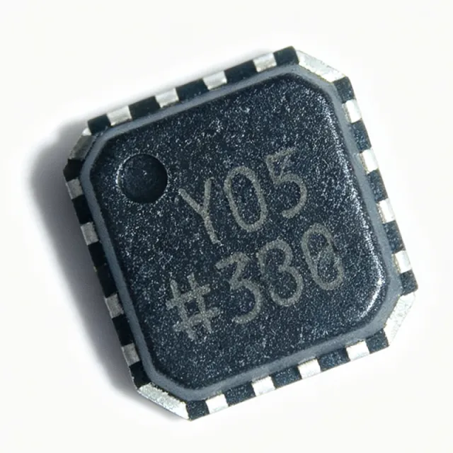
ADCLK905 - Ultrafast SiGe ECL Clock/Data Buffer | Analog Devices
The ADCLK905 is an ultrafast clock/data buffer fabricated on Analog Devices' proprietary XFCB3 silicon germanium (SiGe) bipolar process. It features one input and one output, with full-swing emitter coupled logic (ECL) output drivers. Key specifications include a 95 ps propagation delay, 7.5 GHz toggle rate, 60 ps typical output rise/fall time, and 60 fs random jitter (RJ). The device operates over an extended industrial temperature range and includes on-chip terminations at both input pins. It is available in a 16-lead LFCSP (VQFN) package with exposed pad, suitable for high-speed signal distribution in test and measurement, communications, and data acquisition systems. A clock/data buffer is a high-speed integrated circuit that receives a clock or data signal and re-drives it to one or more outputs with minimal added jitter and propagation delay. It is a critical component in signal distribution networks, ensuring signal integrity across multiple loads. The ADCLK905 belongs to the category of clock buffers, which are part of the broader clock and timing IC family. These devices are essential in systems where precise timing and low jitter are paramount, such as in high-speed ADCs, DACs, and serial data links. Key features of the ADCLK905 include its 7.5 GHz toggle rate, which enables distribution of very high-frequency clocks, and its 60 fs random jitter, which preserves signal integrity in demanding applications. The 95 ps propagation delay ensures minimal latency, and the on-chip terminations simplify PCB layout by reducing external component count. The ECL output drivers provide full-swing signals compatible with ECL logic levels, and the extended industrial temperature range (-40°C to +125°C) supports harsh environments. Technically, the ADCLK905 leverages the XFCB3 SiGe bipolar process, which offers high-speed performance with low power consumption. The device includes a differential input and output, allowing for flexible signal routing. The on-chip terminations at both input pins reduce reflections and improve signal quality. The LFCSP package with exposed pad provides excellent thermal performance, enabling reliable operation at high frequencies. Typical applications include clock distribution for high-speed ADCs and DACs, data buffering in serial communication links, and signal conditioning in test and measurement equipment. The ADCLK905 is also suitable for use in RF and microwave systems where low jitter and high toggle rates are critical. When designing with the ADCLK905, it is important to use high-quality PCB materials and proper termination techniques to maintain signal integrity at multi-gigahertz frequencies. The evaluation board uses high-quality dielectric material between layers to ensure optimal performance.

CDCLVP110VFR - 1:10 LVPECL/HSTL Clock Driver | Texas Instruments
The Texas Instruments CDCLVP110VFR is a low-voltage 1:10 LVPECL/HSTL to LVPECL clock driver that distributes one differential clock input pair to ten differential LVPECL clock outputs with minimum skew. It operates at frequencies up to 3.5 GHz and is available in a 32-pin LQFP package. The device features a selectable input multiplexer that accepts either LVPECL or HSTL input signals, making it versatile for various high-speed clock distribution applications. A clock driver is an integrated circuit that buffers and distributes clock signals to multiple loads while maintaining signal integrity and minimizing skew. It sits between a clock source, such as an oscillator or PLL, and the downstream components that require synchronized timing. Clock drivers are essential in high-speed digital systems where precise timing is critical, such as data converters, FPGAs, and networking equipment. Key features of the CDCLVP110VFR include a 2:10 configuration (two inputs, ten outputs), support for LVPECL and HSTL input standards, and fully compatible outputs with LVECL/LVPECL/HSTL logic levels. The device operates from a single supply voltage, simplifying power design. It is characterized for operation from -40°C to 85°C, making it suitable for industrial environments. The CDCLVP110VFR uses a differential input structure to reject common-mode noise, ensuring clean clock distribution even in noisy environments. The selectable input multiplexer allows the user to choose between two clock sources, providing redundancy or frequency selection. The outputs are designed to drive 50-ohm transmission lines, and the device includes a VBB reference voltage output for single-ended input operation, though differential mode is recommended for high-speed performance. Typical applications include clock distribution for high-speed ADCs/DACs, FPGA and ASIC clocking, networking switches and routers, and test and measurement equipment. The device's low skew and high frequency capability make it ideal for systems requiring synchronized multi-channel operation. When designing with the CDCLVP110VFR, ensure proper termination of the differential outputs and bypass the power supply pins with decoupling capacitors. For single-ended input, connect the VBB pin to CLK0 with a 10-nF bypass capacitor to ground. For optimal performance up to 3.5 GHz, use differential mode.

LMK00306SQX/NOPB - 3.1GHz 6-Output Clock Buffer | Texas Instruments
The Texas Instruments LMK00306SQX/NOPB is a 3.1-GHz differential clock buffer/level translator with 6 configurable outputs, designed for high-frequency, low-jitter clock and data distribution. It is housed in a 36-pin WQFN (NJK) package with an exposed pad, operating over a temperature range of -40°C to 85°C. The device accepts two universal inputs or one crystal input, and distributes the selected clock to two banks of three differential outputs plus one LVCMOS output, providing flexible level translation between LVPECL, LVDS, and HCSL standards. A clock buffer is a component that takes an input clock signal and generates multiple output copies with minimal added jitter and skew, ensuring signal integrity across multiple loads. It sits between a clock source (such as an oscillator or PLL) and downstream devices like ADCs, FPGAs, and SERDES, forming a critical part of the clock distribution network in high-speed digital systems. The LMK00306 belongs to the clock buffer family, which is a subset of clock and timing ICs within the broader semiconductor category. Key features include ultra-low additive jitter of 50 fs RMS (typical) at 100 MHz, a wide input frequency range up to 3.1 GHz, and independent output bank power supplies (VCCO) for level translation. The device supports 3:7 fanout (3 inputs, 7 outputs) and offers pin-programmable output modes, making it highly configurable. Its low additive jitter ensures minimal degradation of the clock signal, critical for high-speed data converters and networking equipment. Technically, the LMK00306 uses a differential input stage with internal termination resistors, and each output bank can be independently configured for LVPECL, LVDS, or HCSL signaling. The device includes an LVCMOS output for low-frequency monitoring or system clocking. The WQFN package with exposed pad provides excellent thermal performance, and the device operates from a 3.3V supply with separate VCCO pins for output level shifting. Typical applications include clock distribution for high-speed ADCs/DACs, FPGA and ASIC clocking, networking switches and routers, and test and measurement equipment. Its low jitter and flexible level translation make it ideal for systems requiring precise timing across multiple boards. When designing with this device, ensure proper termination of unused outputs and place decoupling capacitors close to each power pin. The exposed pad must be soldered to a thermal via array for optimal heat dissipation.