FPGA & CPLD
Products (6357)

EP2C8AF256A7N - Cyclone II FPGA, 8K LE, 256-FBGA | Intel / Altera
The Intel (formerly Altera) EP2C8AF256A7N is a low-cost Cyclone II Field-Programmable Gate Array (FPGA) in the 256-ball FineLine BGA (FBGA) package, offering 8,256 logic elements, 165,888 bits of embedded RAM, and 182 user I/O pins. The 'A7' speed grade and 'N' suffix indicate an industrial/automotive operating temperature grade, manufactured on TSMC's 90 nm process with a 1.2 V core supply, and the device supports up to 402.58 MHz internal operation per the published datasheet. A Field-Programmable Gate Array (FPGA) is a type of programmable logic device (PLD) that lets designers configure digital logic blocks, interconnect, and I/O behavior after PCB fabrication. Within the programmable logic taxonomy, FPGAs sit above simple CPLDs and below ASICs in terms of integration density, offering hundreds of thousands of logic gates, embedded memory blocks, hardware multipliers, and high-speed transceivers in a single chip. The Cyclone II family targets cost-sensitive, high-volume applications such as consumer electronics, automotive infotainment, and industrial control, where designers need ASIC-class logic density without the NRE cost of a custom mask set. Key Cyclone II features include 4-Kbit M4K embedded RAM blocks, dedicated 18-bit x 18-bit hardware multipliers for DSP functions, up to four PLLs per device for clock management, and support for external memory interfaces including DDR, DDR2, and QDR II SRAM. The 'A' in the part number denotes the 1.5 V I/O standard support, while 'F256' indicates the 256-ball FBGA package and 'A7N' specifies the speed/temperature grade. Per the datasheet, the EP2C8A variant specifically supports 182 maximum user I/O pins across four I/O banks. Typical applications span digital video processing, automotive driver-assist subsystems, industrial machine control, motor and power conversion controllers, software-defined radio front-ends, and embedded display interfaces. The combination of low unit cost, automotive temperature support, and 1.2 V low-power operation also makes it well suited for portable and battery-powered embedded systems. When designing with this device, note that the 256-FBGA package requires 1.0 mm ball pitch and a multi-layer PCB with via-in-pad or microvia technology for reliable assembly. Designers should also follow the Altera power sequencing requirements (VCCINT before VCCIO, or use a sequenced supply) to avoid latch-up. For new designs, note that the Cyclone II family is in legacy status and engineers should consider Cyclone IV or Cyclone V for active production programs. This page synthesizes distributor pricing, automotive-grade variants, and practical design notes for the EP2C8AF256A7N that are not found in the manufacturer datasheet alone.
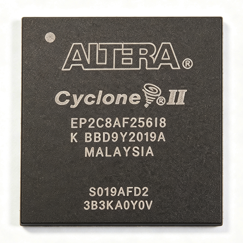
EP2C8AF256I8N - Cyclone II FPGA, 8256 LEs, 256-FBGA | Intel
The Intel (Altera) EP2C8AF256I8N is a low-cost Cyclone II Field Programmable Gate Array built on a 90 nm CMOS process, delivering 8,256 logic elements, 182 user I/O pins, and 165,888 bits of embedded RAM in a 256-ball FineLine BGA package with industrial temperature grade (-40C to +100C). The device is part of Intel's legacy Cyclone II family targeting high-volume, cost-sensitive digital logic integration. What is an FPGA? A Field Programmable Gate Array is a programmable logic device that lets engineers implement arbitrary digital circuits after PCB fabrication, in contrast to an ASIC (Application-Specific Integrated Circuit) whose function is fixed at the foundry. FPGAs sit in the broader taxonomy of programmable logic devices (PLDs) > FPGAs > SRAM-based FPGAs > low-cost FPGAs, alongside SPLDs and CPLDs. Cyclone II occupies the entry-level/low-density node of this hierarchy, optimized for cost-per-logic-element rather than raw performance. Key features include 36 embedded 18x18 multipliers (typical), up to 4 PLLs for clock management, support for external memory interfaces including DDR/DDR2/QDRII SRAM, and configuration via passive serial, active serial, or JTAG. The 1.2 V core supply with separate VCCIO banks (1.5 V / 1.8 V / 2.5 V / 3.3 V) allows mixed-voltage I/O without level shifters, which is a major advantage over older FPGAs with fixed I/O standards. The Cyclone II architecture combines a 2-D row/column interconnect with embedded multiplier blocks and M4K RAM blocks (4 Kbit each, true dual-port), enabling efficient DSP and buffer implementations. 90 nm process technology balances leakage and performance for the target industrial and consumer segments. Typical applications include industrial motor control, video processing bridges, low-cost PCIe endpoints, protocol bridging (UART/SPI/I2C aggregation), and LED display controllers. Designers choose Cyclone II when unit cost matters more than absolute logic density or transceiver speed. Design consideration: PCB layout for a 256-ball FBGA demands 4 to 6 layer stackups with matched-impedance routing for clock and high-speed I/O. The I suffix in the part number denotes the industrial temperature range, which is the appropriate selection for non-automotive applications operating between -40C and +100C. This page synthesizes distributor pricing, drop-in same-package alternatives, and practical design notes that go beyond the manufacturer datasheet to support rapid BOM decisions.
EP2C8F256C6 - Cyclone II FPGA 8K LE 256-FBGA | Intel / Altera
The Intel (formerly Altera) EP2C8F256C6 is a low-cost, low-power Cyclone II Field-Programmable Gate Array (FPGA) housed in a 256-ball FineLine Ball-Grid Array (FBGA) package, integrating 8,256 logic elements, 182 user I/O pins, and 165,888 bits of embedded RAM. It is built on a 90 nm low-k dielectric CMOS process, supports hot-socketing, and is offered in a commercial temperature grade, making it a flexible platform for high-volume cost-sensitive digital designs. The device also embeds up to 36 embedded 18x18 multipliers (typical Cyclone II EP2C8 configuration) for DSP-centric signal processing tasks. An FPGA (Field-Programmable Gate Array) is a type of programmable logic device that allows engineers to implement arbitrary digital logic functions through a sea of configurable logic blocks, embedded memory, and routing resources that are post-fabrication programmed via an SRAM configuration bitstream. FPGAs sit between fixed-function ASICs (high NRE, low unit cost) and discrete logic (flexible but bulky), and within the broader semiconductor taxonomy they belong to programmable logic devices (PLDs) within the digital logic IC category. Cyclone II specifically targets the low-power, low-cost segment where FPGAs previously could not compete with microcontrollers or DSPs on price. Key features of the EP2C8F256C6 include 8,256 logic elements, 36 embedded 18x18 multipliers (typical), 165,888 RAM bits organized into M4K memory blocks, 182 user I/O pins distributed across multiple I/O banks, 4 phase-locked loops (PLLs) for clock management, support for LVDS, LVTTL, LVCMOS, SSTL, and HSTL I/O standards, and configuration via active serial (AS), passive serial (PS), or JTAG interfaces. The 256-FBGA package offers a compact 17x17 mm footprint suitable for space-constrained board layouts. The Cyclone II architecture separates logic into Logic Array Blocks (LABs) of 16 logic elements each, with a 4-input look-up table (LUT), carry chain, and register per logic element. The embedded M4K memory blocks can be configured as SRAM, ROM, or FIFO, while the embedded multipliers accelerate DSP functions such as FIR filters without consuming general-purpose logic. Typical applications for the EP2C8F256C6 include industrial motor control, video processing and display bridging, low-cost DSP co-processing, glue logic replacement, communications protocol bridging (UART, SPI, I2C, PCIe soft cores), and educational/development platforms. The combination of moderate logic density, embedded multipliers, and abundant I/O makes it well suited to mid-complexity designs where a microcontroller lacks throughput but a high-end FPGA is over-spec and over-budget. When designing with this device, ensure that configuration mode (AS/PS/JTAG) is selected to match your system's boot topology, and verify I/O bank voltage compatibility for mixed-voltage interfaces. The 256-FBGA package requires a 1.0 mm or finer pitch PCB land pattern and reflow profile compliant with JEDEC J-STD-020 moisture sensitivity level handling.
EP2C8F256C6N - Cyclone II FPGA, 8K LEs, 256-FBGA | Altera
The Altera (Intel) EP2C8F256C6N is a Cyclone II Field-Programmable Gate Array (FPGA) featuring 8,256 logic elements, 165,888 bits of embedded RAM, and 182 user I/Os, housed in a 256-ball FineLine BGA (FBGA) package. It is built on a low-power 90nm process and targets cost-sensitive, volume-driven digital logic applications where a true FPGA fabric is required rather than a fixed-function ASIC. A Field-Programmable Gate Array is a semiconductor integrated circuit containing an array of configurable logic blocks (CLBs), programmable interconnect, and I/O cells, all of which can be re-defined by the user after manufacture via a hardware description language (HDL) bitstream. FPGAs sit in the broader hierarchy of programmable logic devices (PLD) and bridge the gap between fixed-function ASICs and microcontrollers, offering parallelism, deterministic timing, and the ability to implement custom data-path, glue-logic, and DSP functions in a single device. Key features of the EP2C8F256C6N include 18 embedded 18x18 multipliers for DSP, up to 250 MHz internal operation, support for DDR/DDR2/QDRII memory interfaces via dedicated PHY, four phase-locked loops (PLLs), and a 1.2V core supply. The device is supported by the Quartus II design suite and is shipping in volume today, although Intel has since launched newer Cyclone families (Cyclone III/IV/V) as drop-in successors. Engineers migrating from Cyclone II typically move to Cyclone IV E for the closest functional compatibility and 1.2V core voltage. Typical applications include industrial control and factory automation, video surveillance and image processing, automotive infotainment and driver-assistance, telecommunications line cards, consumer electronics glue logic, and low-volume ASIC prototyping. The 182 user I/Os make it well suited for bridging multiple bus standards (PCI, I2C, SPI, parallel video) in a single device. When designing with this device, verify that the 256-FBGA PCB land pattern is already in your library and confirm the I/O bank voltage (3.3V LVCMOS/LVTTL) matches your downstream memory and peripheral interfaces. Plan for a JTAG header (10-pin or 20-pin) for in-system programming via the Quartus II Programmer. Note that the -C6 speed grade (6 = slowest commercial) limits Fmax compared to -C7 or -C8 variants. This page synthesizes distributor pricing, drop-in compatible variants, and design considerations curated from the manufacturer datasheet and authorized distributor listings to help engineers shorten the component-selection cycle.
EP2C8F256C7 - Cyclone II FPGA, 8K LEs, 256-FBGA | Intel
The Intel (formerly Altera) EP2C8F256C7 is a low-cost Cyclone II field-programmable gate array (FPGA) built on a 90 nm CMOS process, offering 8,256 logic elements, 182 user I/Os, and 165,888 bits of embedded RAM in a 256-ball FineLine BGA (FBGA-256) package. The device operates across commercial temperature grades and supports up to 250 MHz internal operation with embedded multipliers and a four-phase PLL for clock management. An FPGA (Field-Programmable Gate Array) is a semiconductor device whose logic fabric, interconnect, and I/O are configured by the customer after manufacture. FPGAs sit in the broader hierarchy of programmable logic devices (PLD) alongside CPLDs, and they occupy the middle ground between fixed-function ASICs and software-driven processors — offering hardware parallelism, deterministic timing, and the ability to re-spin logic without respinning silicon. The Cyclone II family specifically targets cost-sensitive, high-volume applications where designers need the flexibility of FPGA fabric without paying the silicon-area premium of high-end FPGAs. Key features include 8,256 logic elements (LEs), 36 embedded 18x18 multipliers, 165,888 bits (about 20 Kbytes) of M4K embedded memory blocks, two PLLs for clock multiplication and phase shifting, and 182 maximum user I/O pins supporting LVDS, LVTTL, LVCMOS, SSTL, and PCI I/O standards. Configuration is supported through JTAG, Active Serial (AS), Passive Serial (PS), and Fast Passive Parallel (FPP) modes. The device is supported by the Quartus II design software. Architecturally, the Cyclone II family uses a 1.2 V core supply with separate VCCIO banks for mixed-voltage I/O, allowing the FPGA to bridge between 1.5 V, 1.8 V, 2.5 V, 3.3 V, and differential I/O domains on the same die. The fabric consists of 4-input look-up tables arranged in logic array blocks (LABs), with dedicated routing, embedded multiplier blocks for DSP, and M4K memory blocks that can be configured as RAM, ROM, or FIFO. The 'C7' speed grade denotes a specific Fmax bin relative to other Cyclone II speed grades. Typical applications include industrial motor and motion control, video processing and display bridges, telecommunications line cards, low-cost prototyping for ASIC replacement, and educational / DSP development kits. The 256-FBGA package provides sufficient I/O count for memory-bus and parallel-data interfaces while still being hand-solderable with reflow and hot-air rework for prototypes. Design considerations include careful decoupling of the 1.2 V core and VCCIO bank supplies, length-matched routing for LVDS pairs, and management of the four PLL power pins. The device is in the mature phase of its lifecycle — designers should verify long-term availability before committing to high-volume production. This page synthesizes lifecycle status, drop-in same-brand alternatives, and practical design notes not aggregated on any single distributor listing.
EP2C8F256C7N - Cyclone II FPGA 8K LE 182 I/O | Altera
The Altera EP2C8F256C7N is a Cyclone II Field Programmable Gate Array (FPGA) that integrates 8,256 logic elements, 165,888 RAM bits, and 182 user I/Os in a 256-ball LBGA package. This Pb-free (N) version uses speed grade 7 and a commercial temperature grade, delivering a low-cost, low-power programmable platform for high-volume applications. An FPGA is an integrated circuit whose logic fabric can be reprogrammed after manufacturing, allowing hardware designers to implement custom digital functions, parallel processing datapaths, and glue logic without committing to an ASIC. FPGAs sit above simple programmable logic devices (CPLDs) and below custom silicon, offering flexibility and rapid iteration for communications, industrial, video, and test systems. Within the Altera programmable logic family, Cyclone II was optimized for cost-sensitive applications. The EP2C8F256C7N provides 8,256 logic elements for combinatorial and sequential logic, 165,888 bits of embedded RAM for FIFOs and buffers, and 182 user I/Os configurable for LVTTL, LVCMOS, and other I/O standards. The 256-ball FineLine BGA package keeps board area small while enabling 182 user I/O connections on a low-cost four-layer PCB. Its commercial temperature grade covers typical indoor/consumer installations, and the N suffix indicates lead-free, RoHS-friendly finish. Altera/Intel Cyclone II FPGAs use a predictable architecture with embedded memory, dedicated carry chains, global clocks, and configuration from external serial configuration devices. The speed grade 7 bin occupies a middle point in the family, offering adequate timing performance for mainstream control and DSP-oriented functions while reducing cost relative to faster -6 devices. This architecture is supported in Intel/Altera Quartus for synthesis, fitting, and timing analysis. Typical applications include industrial motor control, video frame capture, test-and-measurement front ends, and communication line cards. In an image-processing design, for instance, the 182 I/Os can interface with CMOS image sensors and memory buses while the embedded RAM buffers pixel lines for filtering. The high usable I/O count makes the EP2C8F256C7N a universal bridge between mixed-signal front ends and digital back ends. A key design consideration is the selection of power supplies: separate the core rails, I/O rails, and PLL supplies with adequate decoupling, and follow Intel/Altera pin-connection guidelines for the 256-LBGA ball map. If RoHS compliance is required, avoid the leaded-solder C7 variant and choose the N version featured here. This page provides distributor pricing, same-family drop-in alternatives, and practical FPGA design notes that supplement the manufacturer Cyclone II datasheet, helping engineers compare parts, verify availability, and plan configuration and power delivery.
EP2C8F256C8 - Cyclone II FPGA, 8K LEs, 256-LBGA | Intel (Altera)
The Intel (formerly Altera) EP2C8F256C8 is a low-cost Cyclone II Field Programmable Gate Array delivering 8,256 logic elements, 165,888 bits of embedded RAM, and 182 user I/O pins in a 256-ball FineLine BGA (LBGA) package. It is built on a 1.2 V, 90 nm SRAM process and supports commercial-temperature (C8) operation at 0 °C to +85 °C. A Field Programmable Gate Array (FPGA) is a semiconductor device whose digital logic, interconnect, and I/O behavior are defined by user-supplied configuration data rather than at the fab. FPGAs sit at the top of the programmable logic taxonomy: programmable logic -> PLD -> CPLD -> FPGA, and they are widely used as glue logic, accelerator fabric, and DSP co-processors alongside microcontrollers and ASICs. The Cyclone II family specifically targets cost-sensitive high-volume applications such as consumer electronics, industrial control, and display bridging. Key features of the EP2C8F256C8 include 8,256 logic elements (LEs), 165,888 bits (~20 Kbytes) of embedded M4K memory blocks, 36 embedded 18 x 18 multipliers for DSP operations, four phase-locked loops (PLLs) for clock management, and 182 maximum user I/O pins. The device supports multiple I/O standards including LVTTL, LVCMOS, PCI, SSTL, and LVDS, providing flexibility for mixed-voltage system designs. Configuration is via active serial (AS), passive serial (PS), or JTAG interfaces, allowing fast prototyping and field updates. Architecturally, Cyclone II FPGAs use 4-input look-up tables (LUT4) and a routing fabric optimized for the 90 nm process node. The M4K memory blocks can be configured as RAM, ROM, or FIFO with true dual-port capability, and the embedded multipliers handle DSP tasks such as FIR filters and FFT butterflies without burning logic resources. The four PLLs provide clock multiplication, division, phase shifting, and zero-delay buffering, which simplifies board-level clock tree design. Typical applications include industrial motor control, video processing and display bridges, automotive infotainment pre-processing, low-cost ASIC prototyping, communications line cards, and portable consumer devices. The wide I/O count and embedded DSP blocks make the EP2C8F256C8 especially well suited for parallel sensor aggregation and mid-density glue-logic functions. Designers should note that the Cyclone II family is a mature node - designers targeting new designs should evaluate the current Cyclone IV/V/10 families for active support. When designing with this device, ensure that the configuration mode pins are pulled to the correct state at power-up and that the JTAG chain is properly terminated to avoid boundary-scan failures. The 256-LBGA FineLine BGA package requires careful PCB layout to manage routing density and thermal dissipation. This page synthesizes distributor pricing, drop-in alternatives within the Cyclone II family, and practical design notes not found in the manufacturer datasheet alone.
EP2C8F256C8N - 8K Logic Elements FPGA | Altera | Embedded Logic
Altera EP2C8F256C8N is a Cyclone II field-programmable gate array containing 8,256 logic elements, 165,888 memory bits, and 182 programmable I/O, supplied in a 256-LBGA package. Its configurable logic and embedded memory support digital control, interface bridging, protocol handling, and glue-logic applications where a fixed ASIC is unnecessary. The FPGA is identified as a 3.3 V device in available comparison information, and exact operating limits must be confirmed from the manufacturer datasheet before design release. A field-programmable gate array is an integrated circuit whose logic functions are defined through configuration rather than fixed wafer-level interconnect. Within the semiconductor hierarchy, the EP2C8F256C8N belongs to FPGA and CPLD devices, which are programmable logic ICs. An FPGA typically combines configurable logic blocks, routing resources, I/O elements, and embedded memory. This flexibility allows engineers to revise functionality, correct design errors, or consolidate several support functions into one device. The principal verified parameters are 8,256 logic elements and 165,888 bits of embedded memory. The device also exposes 182 I/O according to the DigiKey and Heisener listings. The 256-LBGA package provides a large, fine-pitch BGA interface suitable for board designs with substantial external connectivity. Configuration is nonvolatile in the deployment sense because the programmed logic is loaded into the device, but the supplied search data does not state the exact configuration interface, supported memory mode, or startup behavior. Cyclone II devices are suited to datapath, state-machine, communications-control, and embedded system integration functions. The 8,256-logic-element capacity is appropriate for medium-complexity logic, while the 182 I/O count supports multiple buses and peripheral interfaces. Exact logic performance depends on routing, implemented architecture, speed grade, I/O standards, and power supply conditions, none of which are fully specified in the supplied evidence. Typical uses include industrial control, test equipment, image-processing front ends, communications controllers, and educational or legacy FPGA platforms. Its value is strongest when programmability, rapid iteration, and interface consolidation matter more than the very highest logic density. Because the part belongs to an established legacy family, buyers should verify lifecycle status, available configuration support, and long-term supply requirements before new production commitments. Designers should validate the official pin assignment, configuration schematic, decoupling network, supported I/O standards, clock topology, and thermal layout against the manufacturer documentation. The available web material provides basic identity, capacity, I/O count, and package information but does not contain enough authoritative detail to safely invent all missing electrical characteristics. This page combines verified distributor facts, same-package cross-reference evidence, procurement signals, and practical selection guidance without presenting unsupported specifications as datasheet values.
EP2C8F256CX1VAA - Cyclone II FPGA, 8K LEs, 256-FBGA | Altera
The Altera (now Intel) EP2C8F256CX1VAA is a Cyclone II family field-programmable gate array (FPGA) housed in a 256-ball FineLine BGA package. It integrates 8,256 logic elements, 36 M4K RAM blocks (162 Kbits total embedded memory), and 18 embedded 18x18 multipliers, targeting low-cost, high-volume applications across industrial, consumer, and communications segments. The device is fabricated on a 1.2V, 90 nm low-k dielectric CMOS process and supports both commercial and industrial temperature grades. A Field-Programmable Gate Array (FPGA) is a semiconductor device built around a matrix of configurable logic blocks (CLBs) connected via programmable interconnect. FPGAs belong to the broader programmable logic device (PLD) hierarchy, sitting alongside CPLDs and structured ASICs. They differ from microcontrollers (which execute sequential firmware) by implementing logic in hardware, parallel by construction, and differ from ASICs by being reconfigurable after manufacture. Cyclone II sits in the low-cost end of the FPGA market, optimized for ASIC replacement and DSP co-processing rather than maximum density or highest clock rate. Key features include up to 4 PLLs, 8 global clock networks, support for LVDS, LVTTL, PCI, SSTL, and other single-ended and differential I/O standards, and high-speed external memory interfaces including DDR/DDR2/QDRII SRAM. The device supports configuration via passive serial, active serial, and JTAG modes, with built-in decompression and decryption engines to accelerate bitstream transfer. Typical applications include digital signal processing, video processing pipelines, industrial machine control, motor control, automotive infotainment subsystems, and protocol bridging between legacy and modern interfaces. Cyclone II devices are commonly paired with external DDR/DDR2 memory and TI power management ICs such as the TPS5430 for core and I/O rail generation. When designing with this device, ensure proper power sequencing (VCCINT must precede VCCA/VCCIO), adequate thermal dissipation through the BGA thermal ball pattern, and pin-compatible migration paths if upgrading to Cyclone III or Cyclone IV. The EP2C8F256CX1VAA suffix indicates a 256-ball FBGA, industrial temperature grade, and lead-free / RoHS compliant packaging.
EP2C8F256CXN - Cyclone II FPGA, 8K LEs, 256-FBGA | Altera
The Altera (now Intel PSG) EP2C8F256CXN is a Cyclone II series Field-Programmable Gate Array (FPGA) housed in a 256-ball FineLine Ball-Grid Array (FBGA) package. Built on a low-power 90 nm process, this device delivers 8,256 logic elements, 165,888 bits of embedded RAM, and 182 user I/O pins with support for multiple I/O standards including LVDS, LVTTL, LVCMOS, SSTL, and PCI. A Field-Programmable Gate Array (FPGA) is a programmable logic IC containing an array of configurable logic blocks (CLBs), programmable interconnect, and I/O cells, all fabricated on a single silicon die. FPGAs occupy a position in the broader hierarchy of digital semiconductors: programmable logic > logic ICs > integrated circuits > semiconductors. They are typically deployed as glue logic, signal-processing engines, or prototyping platforms where ASIC NRE costs cannot be justified. Key features include 18 embedded 18x18 multipliers, two PLLs for clock management, and configuration support via active serial (AS), passive serial (PS), and JTAG modes. The device operates from a 1.15 V to 1.25 V core supply with separate VCCIO banks for I/O standard flexibility. The 256-FBGA package offers a compact footprint suitable for space-constrained designs while maintaining sufficient pin count for high-I/O applications. The Cyclone II architecture is built on SRAM-based configuration memory, requiring an external configuration device for standalone operation. The device family is positioned as a low-cost, low-power alternative to ASICs in volume production for applications such as industrial control, video processing, and communications infrastructure. Typical applications include motor control, video bridging, industrial Ethernet gateways, and educational/hobbyist development. The 182 user I/O count makes it well-suited for designs that aggregate multiple peripheral interfaces (UART, SPI, I2C, parallel buses) onto a single programmable device. When designing with this FPGA, ensure the configuration scheme is selected based on the number of devices on the JTAG chain and whether in-system programmability is required. The 256-FBGA package requires careful PCB layout with appropriate via-in-pad or microvia technology to avoid solder joint defects during reflow. This page synthesizes distributor stock levels, parametric drop-in alternatives from the same Cyclone II family, and PCB layout guidance not typically consolidated on a single manufacturer product page.
EP2C8F256CXNAA - Cyclone II FPGA 8K LE, 256-FBGA | Intel
The Intel (formerly Altera) EP2C8F256CXNAA is a low-cost Cyclone II field-programmable gate array (FPGA) offering 8,256 logic elements, 162 Kbits of embedded RAM, and 18 embedded 18x18 multipliers in a 256-ball FineLine BGA package. It is a lead-free, RoHS-compliant variant of the EP2C8 family, providing up to 182 user I/O pins with 4 phase-locked loops and a maximum user flash memory of 0 Kbits. The device operates from a 1.15V to 1.25V core supply with 3.3V/2.5V/1.8V/1.5V LVCMOS/LVTTL I/O support. A field-programmable gate array (FPGA) is a semiconductor integrated circuit built around a matrix of configurable logic blocks (CLBs) connected by programmable interconnect. FPGAs belong to the broader category of programmable logic devices (PLDs), which sit within the integrated circuit (IC) hierarchy alongside ASICs, microcontrollers, and DSPs. Cyclone II FPGAs specifically target cost-sensitive, high-volume applications and represent the second generation of Altera's low-cost FPGA family. Key features of the EP2C8F256CXNAA include 8,256 logic elements at 90 nm process technology, 36 M4K RAM blocks (4,608 bits each) totaling 162 Kbits, 18 dedicated 18x18 hardware multipliers for DSP operations, and 4 PLLs for clock management. The device supports configuration via active serial (AS), passive serial (PS), and JTAG modes, with 0 Kbits of on-chip user flash memory. Its 256-ball FBGA package uses a 1.0 mm ball pitch and is RoHS compliant. Architecturally, Cyclone II FPGAs use a lookup-table (LUT)-based logic fabric with embedded memory columns and multiplier blocks distributed across the die. The four PLLs support clock multiplication, division, phase shifting, and external clock output, enabling complex multi-clock domain designs. The 18x18 multipliers accelerate DSP functions such as FIR filters, FFTs, and video processing without consuming general-purpose logic resources. Typical applications include digital signal processing, video processing pipelines, industrial control and factory automation, communications protocol bridging, motor control, and consumer electronics prototyping. The combination of low unit cost, moderate logic density, and integrated DSP blocks makes the EP2C8 ideal for glue logic replacement, custom peripheral interfacing, and parallel processing tasks. A specific use case is LED video wall controllers, where the 18 multipliers handle brightness/color scaling and the 162 Kbits of RAM buffer scan-line data. When designing with this part, pay close attention to the four independent PLL blocks - they require dedicated power pins (VCCA_PLL) and ground isolation, and each PLL has a dedicated analog supply of 1.2V. The 256-FBGA package is a wirebond BGA with 1.0 mm pitch, requiring PCB design with microvia technology (not compatible with 6/6 mil standard 2-layer boards). Use Intel Quartus II for synthesis, place-and-route, and configuration file generation. This page synthesizes distributor pricing, drop-in same-package alternatives from the Cyclone II family, and practical design notes not found in the manufacturer datasheet alone. Engineers evaluating the EP2C8F256CXNAA for new designs should note that Cyclone II is a mature, end-of-life family, so long-term availability planning is essential.
EP2C8F256I6N - Cyclone II FPGA, 8256 LEs, 256-BGA | Intel
The Intel (formerly Altera) EP2C8F256I6N is a Cyclone II family Field Programmable Gate Array (FPGA) housed in a 256-ball FineLine BGA (FBGA-256) package. The device integrates 8,256 logic elements organized into 540 logic array blocks (LABs), 165,888 bits of on-chip embedded RAM (M4K blocks), and up to 182 user I/O pins, all fabricated on a low-power 90 nm CMOS process with a 1.2 V core supply and a maximum internal clock frequency rated to 402 MHz. The "I6" speed grade in this datasheet designation denotes the industrial operating range (-40 °C to +100 °C junction), while the "N" suffix indicates a lead-free, RoHS-compliant package. What is an FPGA? An FPGA (Field Programmable Gate Array) is a semiconductor device whose digital logic fabric, routing, and I/O behavior are defined by a user-supplied configuration bitstream rather than at the factory. FPGAs sit at the top of the programmable logic hierarchy (FPGA -> programmable logic -> digital IC -> semiconductor) and are used wherever time-to-market, hardware parallelism, or in-field reconfigurability matters. The Cyclone II family was positioned as Altera's low-cost, high-volume FPGA, competing with Xilinx Spartan-3 in applications such as digital signal processing, video bridging, motor control, and glue-logic consolidation. Key features of the EP2C8F256I6N include 36 embedded 18 × 18 hardware multipliers that support DSP blocks at up to 250 MHz, four phase-locked loops (PLLs) for clock management, and support for external memory interfaces including DDR, DDR2, SDR, and QDRII SRAM. The 256-pin FBGA package provides a 1.00 mm ball pitch and uses the industrial temperature grade for harsher environments. Compared with newer Cyclone IV/V parts, the EP2C8F256I6N trades static power for low unit cost, making it attractive for cost-sensitive, proven designs. In practice the EP2C8F256I6N is used in industrial motor drives, video capture and display pipelines, software-defined radio front-ends, low-density ASIC prototyping, and embedded control boards that require parallel DSP. Its 165 Kbits of block RAM and 18 × 18 multipliers allow moderate-throughput FIR filters and FFTs without external memory for coefficient storage. Designers should review the I/O bank voltage and pin assignment tables in the Cyclone II Device Handbook before layout, since each of the eight I/O banks can be powered independently between 1.5 V and 3.3 V. Configuration modes include JTAG, Active Serial, and Passive Serial, and the Quartus II (or later) toolchain is required for synthesis, fitting, and bitstream generation. This page synthesizes distributor pricing, drop-in same-footprint alternatives from the Cyclone II family, and practical design notes not found in the manufacturer datasheet.
EP2C8F256I8 FPGA - Cyclone II 8256 LE, 256-FBGA | Intel
The Intel (Altera) EP2C8F256I8 is a Cyclone II field-programmable gate array (FPGA) with 8,256 logic elements, 165,888 RAM bits, and 182 user I/O pins, delivered in a 256-ball LBGA/FBGA package. The 'I' suffix denotes an industrial temperature range version and the '8' suffix identifies the speed grade. It is a low-cost, high-volume programmable logic device suited for communication, video, and industrial applications that require post-assembly logic changes and flexible I/O. An FPGA is a semiconductor device containing programmable logic blocks, embedded memory, and programmable interconnects that can be configured after manufacturing. The Cyclone II family sits in Intel/Altera's mainstream programmable logic portfolio between MAX CPLDs and high-end Stratix devices. In product hierarchy terms, EP2C8F256I8 is an FPGA -> programmable logic device -> integrated circuit. Engineers configure the logic array using hardware description languages such as Verilog or VHDL, then download a configuration bitstream through active serial, passive serial, or JTAG interfaces. EP2C8F256I8's 8,256 logic elements provide approximately 516 logic array blocks for custom logic functions. The 165,888 RAM bits are organized in M4K memory blocks and can implement FIFOs, small packet buffers, or dual-port memories for data path applications. The 182 user I/O balls support the flexible I/O levels commonly used for memory buses, backplane interfaces, and video data paths. The 256-ball FineLine BGA form factor keeps the design compact while preserving routing access for multiple I/O banks. Because this is a Cyclone II low-cost family device, it is often paired with serial configuration devices and external memories rather than used as a processor-centric SoC. The industrial temperature option is valuable for equipment installed in uncontrolled environments such as factory floors, base stations, and outdoor signage. The FPGA's reconfigurability also allows field updates through secure or partial reconfiguration flows, which reduces service cost over the product lifetime. Typical applications include industrial motor-control logic, video frame grabbers, protocol bridging between Ethernet and custom buses, and test instruments that need a flexible I/O front end. The 182 I/O pins make it practical to connect to multiple ADCs, DACs, memories, and transceivers in the same design. With 165,888 bits of on-chip RAM, moderate packet buffering and line-rate FIFO functions can be implemented without adding an external SRAM. When designing with EP2C8F256I8, pay attention to the core and I/O power supply rails, configuration voltage requirements, and bypass capacitor placement. The FPGA must be configured from an external configuration device or host after power-up; selecting AS or JTAG mode affects the bill of materials and manufacturing test flow. Keep the configuration clock and data signals clean and short to avoid bitstream corruption during production programming. This page synthesizes distributor inventory, verified specification snippets, drop-in Intel/Altera alternatives, and practical design notes not repeated in every datasheet. Use it as a starting point for a full Cyclone II Handbook review before production.
EP2C8F256I8K - Cyclone II FPGA, 8K LEs, FBGA-256 | Altera / Intel
The Intel (formerly Altera) Cyclone II EP2C8F256I8K is a low-cost, low-power Field-Programmable Gate Array (FPGA) from the Cyclone II family, fabricated on a 90 nm CMOS process and housed in a 256-ball FineLine BGA (FBGA-256) package. It contains 8,256 logic elements, 182 user I/O pins, 36 embedded 18x18 multipliers, and 165,888 bits of embedded RAM, providing a balanced resource mix for cost-sensitive programmable-logic designs. An FPGA (Field-Programmable Gate Array) is a semiconductor device built around an array of configurable logic blocks (CLBs), programmable interconnect, and I/O cells that engineers can reconfigure in the field using an HDL description. Within the broader taxonomy, FPGAs sit alongside CPLDs, microcontrollers, and ASICs as programmable-logic devices; FPGAs are distinguished by high logic density, on-chip memory, DSP blocks, and (in newer families) hardened transceivers. The Cyclone II family targets volume, low-static-power applications such as consumer electronics, industrial control, and display bridging. Key features of the EP2C8F256I8K include support for multiple single-ended I/O standards (LVTTL, LVCMOS, PCI, SSTL, LVDS), up to four PLLs with up to eight outputs for clock management, configurable JTAG boundary-scan, and on-chip bit-stream decryption for design IP protection. The device operates from a 1.2 V core supply with separate VCCIO banks for I/O flexibility, and its commercial-grade -40 °C to +100 °C junction temperature range suits industrial enclosures. Cyclone II devices are SRAM-based and require an external configuration memory, typically an EPCS or EPCQ serial flash. Typical applications include video processing bridges, motor and motion control, industrial protocol converters (RS-485, CAN, Modbus), low-density DSP pre-processing, LED display controllers, and education or evaluation platforms. The EP2C8F256I8K is also a popular choice for legacy design maintenance because it combines a familiar Quartus II development flow with abundant reference designs. When designing with this device, plan power sequencing for VCCINT (1.2 V) and VCCIO banks carefully and respect the 90 nm SRAM volatile-configuration requirement by selecting a robust serial configuration flash. For new designs, evaluate the Cyclone IV or Cyclone V families first for lower static power; for drop-in board reuse of an existing Cyclone II layout, the EP2C8F256I8K remains a reliable choice.
EP2C8F256I8N - Cyclone II FPGA, 8K LEs, 256-FBGA | Intel / Altera
The Intel (formerly Altera) EP2C8F256I8N is a Cyclone II Field Programmable Gate Array (FPGA) with 8,256 logic elements, 165,888 bits of embedded RAM, and 182 user I/O pins, housed in a 256-ball FineLine BGA package. Built on a low-power 90-nm CMOS process, the device operates from a 1.2 V core supply with I/O banks that support LVTTL, LVCMOS, SSTL, and LVDS signaling for direct interface to DDR/DDR2 memory and common parallel peripherals. An FPGA (Field Programmable Gate Array) is a programmable logic device that combines configurable logic blocks, programmable routing, and dedicated silicon resources such as block RAM, DSP blocks, PLLs, and high-speed transceivers. The Cyclone II family is positioned in the low-cost, high-volume tier of the Intel FPGA portfolio (FPGA -> programmable logic -> logic IC -> integrated circuit -> semiconductor), targeting applications where designers need the flexibility of hardware programmability without the NRE of an ASIC. Key features of the EP2C8F256I8N include two general-purpose PLLs for clock synthesis and skew management, up to 36 embedded 18x18 multipliers for DSP operations, and True-LVDS support on selected I/O pins. The device supports the Nios II embedded processor for soft-core CPU integration, allowing complete SoC implementation on a single chip with custom peripherals, memory controllers, and DMA engines. Architecturally, the Cyclone II device uses an SRAM-based configuration cell that must be loaded from an external configuration flash (EPCS) at every power-up. The 256-FBGA (17 mm x 17 mm body, 1.0 mm ball pitch) offers a denser pin-out than TQFP equivalents and exposes more user I/O at the cost of standard SMT assembly processes. Typical applications include industrial machine vision, motor control, video processing, low-cost DSP front-ends, and embedded control systems. Designers also deploy this part as a bridge between legacy parallel buses (PCI, ISA) and modern high-speed serial interfaces where pre-built IP cores accelerate development. A critical design consideration: verify PCB routing rules for the 1.0 mm pitch FBGA, including microvia stack-up and matched-length DDR traces if DDR/DDR2 memory is used. The "I8N" suffix denotes the industrial temperature grade (-40C to +85C) with lead-free (Pb-free) reflow compatibility. This page synthesizes distributor pricing, drop-in Cyclone II alternatives, and practical design notes not found in the manufacturer datasheet alone.

EP2C8Q208 - Cyclone II FPGA, 8256 LE, 208-PQFP | Altera
The Altera (Intel) EP2C8Q208 is a member of the Cyclone II FPGA family fabricated on a 90 nm low-k dielectric CMOS process, delivering 8,256 logic elements in a 208-pin plastic QFP package with 138 user I/O pins. The device integrates 165,888 bits of embedded RAM organized as M4K blocks, 18 embedded 18x18 multipliers for DSP acceleration, and a die that targets cost-sensitive, high-volume logic, control and signal-processing designs. A field programmable gate array (FPGA) is a programmable semiconductor device that implements custom digital logic through configurable logic blocks (CLBs), programmable routing, and dedicated hard IP. FPGAs sit in the broader programmable logic taxonomy between programmable logic devices (CPLDs) and more complex SOCs, and are typically used as glue logic, co-processors, prototyping platforms and small-to-medium digital systems. Cyclone II, introduced in 2004, is positioned as the low-cost, low-power end of the Altera FPGA family tree: Cyclone -> Cyclone II -> Cyclone III/IV/V. Headline features of the EP2C8Q208 include 8,256 logic elements (LEs), 36 M4K memory blocks providing 165,888 bits (about 20 Kbyte) of true dual-port RAM, 18 hardware 18x18 multipliers (delivering up to ~1.3 GMACs at 250 MHz) and 4 PLLs with up to 16 output clock paths. Configuration is via Altera active serial (AS), passive serial (PS) or JTAG modes, supported through dedicated pins on the package. The 208-pin PQFP (often referred to as BFQFP or 208-PQFP) offers 138 user I/O pins, allowing wide parallel buses, memory interfaces and LVDS pairs. Typical applications include industrial control and factory automation backplanes, video processing front-ends, motor control and inverter signal chains, telecom line cards, low-cost DSP pre-processing, and educational / academic hardware platforms such as the DE2 development board. The Cyclone II architecture is supported by Altera's Quartus II design suite (now part of the Intel Quartus Prime toolchain) with reference designs, megafunctions and DSP Builder support. When designing with EP2C8Q208, pay attention to the I/O standard grouping (the 208-PQFP splits I/O into multiple banks with independent VCCIO rails), the LVDS pair count limit per bank, and the 1.2 V core supply requirement. This part is now in the legacy/EOL family tier; new designs should consider Cyclone IV E, MAX 10, or Lattice ECP5 as modern equivalents.
EP2C8Q20818 - Cyclone II FPGA, 8K LEs, 208-Pin PQFP | Intel
The Intel (formerly Altera) EP2C8Q20818 is a Cyclone II family Field-Programmable Gate Array (FPGA) housed in a 208-pin Plastic Quad Flat Pack (PQFP) package, with 8,256 logic elements and 165,888 bits of embedded RAM. Built on a low-power 90-nm process, the EP2C8Q20818 targets cost-sensitive applications requiring moderate logic density and embedded multiplier support without the cost of high-end FPGAs. An FPGA (Field-Programmable Gate Array) is a semiconductor device containing programmable logic blocks, interconnect, and I/O that the designer configures after manufacturing using a hardware description language. FPGAs sit between microcontrollers (sequential, software-driven) and ASICs (fixed-function, high-NRE); they offer hardware parallelism and reconfigurability for DSP, glue logic, and prototype-to-production bridging. Cyclone II belongs to Intel's low-cost FPGA family, hierarchically: FPGA -> programmable logic -> programmable logic IC -> integrated circuit. Key features of the EP2C8Q20818 include 138 user I/O pins supporting multiple I/O standards (LVTTL, LVCMOS, PCI, SSTL, LVDS), up to 36 embedded 18x18 multipliers, 165,888 bits (approximately 20 Kbytes) of M4K embedded memory blocks, and 2 PLLs for clock management. The device supports configuration via active serial (AS), passive serial (PS), and JTAG modes, and is offered in commercial (0C to +85C) and industrial (-40C to +100C) temperature grades. Architecturally, the EP2C8Q20818 uses 4-input look-up tables (LUTs) and embedded M4K RAM blocks, with each M4K block configurable as RAM, ROM, or shift register. The 90-nm CMOS process delivers low static and dynamic power, with multiple low-power operation modes. The device supports Nios II soft-core processor implementation, enabling custom embedded CPU integration in firmware-free logic. Typical applications include industrial control and motor drive logic, video and image processing pipelines, consumer electronics glue logic, telecommunications interface bridging, low-cost DSP front-ends, and educational/development platforms. The Cyclone II family is also widely used in legacy designs and as a low-cost entry into FPGA development for hobbyist and academic use. When designing with the EP2C8Q20818, ensure 3.3V tolerance on I/O banks is properly considered and that the configuration mode matches your selected EPCS or JTAG programmer. Power sequencing requirements follow the standard Cyclone II guidelines, and the device is supported by the Quartus II design software (legacy versions recommended for Cyclone II designs).
EP2C8Q208C7 - Cyclone II FPGA, 8256 LE, 138 I/O | Altera
The Altera EP2C8Q208C7 is a Cyclone II field-programmable gate array (FPGA) containing 8,256 logic elements, 165,888 bits of embedded RAM, and 138 user I/O pins, supplied in a 208-pin BFQFP package. The part is one of the many PQFP208 Cyclone II variants used in cost-sensitive logic, interface, and control designs that require programmable logic without the cost of high-end FPGAs. A field-programmable gate array (FPGA) is an integrated circuit whose digital fabric can be configured after manufacturing by loading a bitstream. Unlike a fixed-function ASIC or microcontroller, an FPGA lets a designer implement parallel hardware logic such as counters, state machines, buses, and DSP functions and revise that logic in the field. The EP2C8Q208C7 belongs to Altera's Cyclone II family, a low-cost SRAM-based FPGA line aimed at applications where logic density, I/O count, and unit price must be balanced. Key features that define the EP2C8Q208C7 include 8,256 logic elements, 138 available user I/Os, and 165,888 bits of on-chip RAM. The 208-pin BFQFP package occupies a conventional quad flat pack footprint and can be used in multilayer boards without BGA routing complexity. The suffix C7 indicates a commercial-temperature ordering grade and speed grade 7, and the non-N finish contains lead, so designs requiring RoHS compliance should select the lead-free N version or another green variant. Distributor pages also list the device at 450 MHz, making it appropriate for moderate-speed control and data-path applications. From an architecture perspective, the EP2C8Q208C7 is an SRAM-based FPGA with look-up-table-based logic blocks, embedded memory blocks, and programmable I/O buffers. Configuration data must be loaded into the device at power-up, and the FPGA can be programmed through JTAG or with an external configuration device. Because the device is part of the mature Cyclone II family, design support remains available through Altera/Intel Quartus software, but new designs should confirm tool-version compatibility and lifecycle support before committing. Typical applications include industrial control, protocol bridging, video and image capture, test equipment, and motor-control logic. The 138 user I/O pins allow multiple parallel buses, encoder interfaces, and low-speed communication ports to be connected in one device, while the embedded memory supports small FIFOs and look-up tables. One key design consideration is that the C7 version is not lead-free: if your manufacturing process or target market requires RoHS compliance, use EP2C8Q208C7N or an I-speed/N version. Also provide proper 0.1uF decoupling on all FPGA rails and load the configuration bitstream from the system controller or a serial configuration device. This page synthesizes distributor availability, pricing tiers, drop-in alternatives, and practical design notes for EP2C8Q208C7 with information drawn from Octopart, DigiKey, Mouser, LCSC, and other public sources, complementing the manufacturer Cyclone II documentation.
EP2C8Q208C7N - Cyclone II FPGA, 8256 Logic Elements | Altera
The Altera EP2C8Q208C7N is a Cyclone II field-programmable gate array (FPGA) with 8,256 logic elements, 165,888 total RAM bits and 138 user I/O pins, delivered in a 208-pin BFQFP (PQFP) surface-mount package. It is an SRAM-based programmable logic device intended for low-cost, medium-density systems where hardware functions can be updated in the field. An FPGA is an integrated circuit whose logic fabric is configured after manufacturing rather than being fixed at the factory. In the product hierarchy, the EP2C8Q208C7N is an FPGA, which is a subclass of programmable logic devices and integrated circuits. Designers describe digital logic in an HDL such as Verilog or VHDL, synthesize it, and load the resulting bitstream into the FPGA. Because the device is SRAM-based, the configuration data is lost at power-off and must be reloaded from an external memory or through a JTAG interface at every power-up. From the verified distributor data, the EP2C8Q208C7N provides 8,256 logic elements, 165,888 total RAM bits, and 138 user I/O pins. This resource level supports moderate combinational and sequential logic, small FIFOs, state machines, soft-core processors, and custom peripherals. The 208-BFQFP package gives design teams a reworkable QFP alternative for systems that do not require a fine-pitch BGA. The seven in the ordering code indicates speed grade -7, and the N suffix represents the lead-free package option used by Altera ordering nomenclature. Technically, the Cyclone II family is a 90 nm SRAM-based FPGA architecture. Its logic cells are suited to designs with modest density requirements, while the embedded memory bits allow on-chip buffering without always adding external SRAM. The 138 user I/O pins can be organized into banks for interfacing with standard logic families and bus interfaces. Exact supported I/O standards, PLL details, configuration pin behavior, and timing tables should be confirmed from the manufacturer datasheet; those silicon-level details are not included in the distributor snippets used on this page. Typical uses include industrial motor control, protocol bridging, small video and image-processing pipelines, LED display control, data acquisition, and medical monitoring front ends. Because of its low-cost QFP format and mature tool flow, it is also used in legacy industrial and communications systems where redesign is undesirable. For high-speed or memory-intensive applications, external SDRAM or higher-density FPGAs are more appropriate. When designing with this FPGA, budget a serial configuration device such as an EPCS flash or provide JTAG configuration during production test. Keep power supplies clean and decoupled close to the FPGA package, and verify the I/O bank voltage before connecting external logic. Treat Cyclone II as a mature product family: for new designs, confirm availability and Intel lifecycle support before committing to a production program. This page synthesizes distributor pricing, package and availability data, practical design notes, and drop-in alternatives that are not all stated on a single distributor page, providing a useful companion to the manufacturer datasheet.
EP2C8Q208C8 - Cyclone II FPGA, 8K LE, 208-Pin PQFP | Intel
The Intel (formerly Altera) EP2C8Q208C8 is a Cyclone II family Field-Programmable Gate Array (FPGA) featuring 8,256 logic elements (540 logic cells / 516 LABs), 138 user I/Os, and 165,888 bits of embedded RAM, housed in a 208-pin Plastic Quad Flat Pack (PQFP / BFQFP) commercial-grade package (0°C to 85°C). The device is fabricated in a low-power 90 nm CMOS process with a 1.2 V core supply and supports configuration via serial or parallel interfaces, making it a workhorse programmable logic device for cost-sensitive volume production. A Cyclone II FPGA belongs to the SRAM-based programmable logic hierarchy: FPGA -> programmable logic device (PLD) -> logic IC -> integrated circuit. Cyclone II sits below Stratix and above MAX in the Altera/Intel portfolio, optimized for high-volume, low-power applications such as digital video, industrial control, and communications glue logic. The 90 nm process delivers a balance between cost, density, and static power that legacy Cyclone designs still leverage today. Key features of the EP2C8Q208C8 include 36 embedded 18×18 multipliers suited for DSP functions, up to four PLLs for clock management, and dual-purpose configuration pins that double as user I/O after configuration. Maximum internal operating frequency is typically 402.5 MHz, with logic capacity sufficient for glue-logic, bridging, and mid-complexity state-machine designs. Typical applications for the EP2C8Q208C8 span industrial control boards, video processing front-ends, low-cost PCIe endpoint bridges, legacy telecom line cards, and educational logic-design platforms. The 138 available I/Os comfortably interface to DDR/DDR2 memory, LVDS, and standard parallel buses. Design entry via Altera/Intel Quartus II software ensures access to a mature IP library including Nios II embedded processors. When designing with the EP2C8Q208C8, ensure proper decoupling (0.1 µF + bulk capacitors per VCCINT/VCCIO bank) and that JTAG chain integrity is maintained for in-system programming. Users migrating from legacy Altera parts should re-validate timing closure in Quartus II, as the design environment has evolved across multiple Quartus releases since this device launched. This page synthesizes distributor pricing, real-time stock, drop-in same-family alternatives, and practical design notes not consolidated in any single manufacturer datasheet, helping engineers evaluate the EP2C8Q208C8 for new designs and long-term maintenance programs.
EP2C8Q208C8N - Cyclone II FPGA 8K LE, 208-QFP | Altera
The Altera EP2C8Q208C8N is a Cyclone II field-programmable gate array (FPGA) with 8,256 logic elements, 165,888 RAM bits and 138 user I/O pins, housed in a 208-pin BFQFP package. It uses a 1.2 V core supply and operates over the commercial temperature range of 0°C to 85°C. Fabricated with 90 nm CMOS process technology, the device provides 402.58 MHz maximum internal clock capability per ADatasheet and Ampheo listings. A field-programmable gate array is an integrated circuit whose logic fabric can be configured after manufacturing by loading an HDL-generated bitstream. Cyclone II is Altera's low-cost 90 nm FPGA family, positioned in the hierarchy FPGA > programmable logic device > digital IC > semiconductor. The EP2C8Q208C8N combines logic elements, embedded RAM and flexible I/O without custom mask costs, allowing designers to prototype and deploy digital systems quickly. In system hierarchy, FPGAs often sit between processors and dedicated ASICs, providing reconfigurable glue logic, protocol bridging and parallel processing. Key features include 8,256 logic elements, 165,888 RAM bits and 138 user I/O channels. The C8 speed grade gives balanced timing performance for many motor-control, video and communication designs. The 1.2 V core supply reduces dynamic power compared with older 1.5 V/1.8 V FPGA families while retaining ample routing resources. A 208-pin BFQFP package is a cost-effective, surface-mount, JEDEC-standard quad flat pack that is easier to route on multilayer PCBs than high-density BGA packages for moderate I/O counts. Architecturally, Cyclone II is an SRAM-based FPGA: configuration data must be loaded at power-up from an external configuration device or host controller. The EP2C8Q208C8N uses a 1.2 V VCCINT, has multiple I/O banks, and belongs to the Cyclone II family documented in Intel-Altera Cyclone II device literature. Because the part is SRAM-based, no state is retained when power is removed, and an external boot source such as an EPCS serial configuration device is required for standalone operation. Typical applications include industrial motor control, video frame capture and preprocessing, communication protocol bridging, digital signal interfacing and FPGA training platforms. With 138 user I/O pins, the EP2C8Q208C8N can implement 8-/16-bit buses, quadrature encoder interfaces, parallel ADCs/DACs and general-purpose control logic in a single programmable device. When designing with this component, place 100 nF decoupling capacitors close to every VCC pin and bulk capacitors on each VCCIO bank. Core voltage is 1.2 V; I/O bank voltages must match the interface standard connected to each bank. Since the package is SRAM-configurable, ensure the MSEL pins and configuration device are correctly wired before first power-up. This page synthesizes distributor stock/price, drop-in Altera-family alternatives, and practical configuration guidance that complements the official Intel-Altera datasheet and the DigiKey/Mouser/LCSC product listings.
EP2C8Q208I8 - Cyclone II FPGA, 8K LEs, 208-QFP | Intel
The Intel EP2C8Q208I8 is a Cyclone II family Field-Programmable Gate Array (FPGA) fabricated on a 90 nm low-k process, delivering 8,256 logic elements and 165,888 bits of embedded RAM in a 208-pin Plastic Quad Flat Pack (PQFP/BFQFP) package. The device exposes 138 user I/O pins, supports up to 36 M4K RAM blocks, and integrates up to 18 embedded 18x18 multipliers, making it suitable for cost-sensitive digital signal processing, glue logic, and parallel data acquisition designs. A Field-Programmable Gate Array (FPGA) is a reconfigurable integrated circuit whose logic fabric, routing, and I/O can be customized by the designer after manufacture. Within the broader semiconductor taxonomy, FPGAs sit alongside microcontrollers, DSPs, and ASICs as a programmable logic device (PLD) category used for prototyping, low-volume production, and applications requiring hardware-level parallelism. The Cyclone II family specifically targets low-power, cost-optimized designs in the industrial, communications, and consumer markets. Key features of the EP2C8Q208I8 include a core supply of 1.2 V with multi-volt I/O support up to 3.3 V LVTTL/LVCMOS, on-chip PLL blocks for clock generation and skew management, and configuration support via JTAG and active serial (AS) modes. The M4K RAM blocks deliver true dual-port operation with parity, while the 18x18 multipliers enable single-cycle DSP operations at system clock rates up to 250 MHz in the I8 industrial speed grade. Architecturally, the device combines a 2D array of logic array blocks (LABs), each containing ten logic elements (LEs) built from 4-input look-up tables (LUTs), with dedicated routing, memory, and multiplier resources. Cyclone II was the first low-cost FPGA family to use a 90 nm process, enabling a substantial density increase over the original Cyclone series while maintaining static power below 0.25 W in typical configurations. Typical applications include industrial control and machine vision, motor drive and inverter control, software-defined radio front-ends, low-cost video processing, and protocol bridging such as UART-to-PCIe or SPI-to-DDR controllers. The 138 available user I/Os comfortably support parallel SRAM/SSRAM and DDR SDRAM interfaces when paired with the dedicated DQS delay lines. When designing with the EP2C8Q208I8, pay attention to power decoupling: place 0.1 uF and 0.01 uF ceramic capacitors near every VCCINT and VCCIO pin, and use a four-layer PCB with a continuous ground plane to control simultaneous-switching-noise (SSN). The I8 speed grade is the industrial-temperature variant operating from -40 C to +100 C case temperature. This page synthesizes distributor pricing, drop-in pin-compatible alternatives in the same 208-pin PQFP footprint, and practical design notes that complement the manufacturer datasheet and accelerate your board bring-up.
EP2C8Q208I8N - Cyclone II FPGA, 8K LEs, 208-PQFP | Altera / Intel
The Altera (Intel) EP2C8Q208I8N is a Cyclone II family Field-Programmable Gate Array (FPGA) delivering 8,256 logic elements and 165,888 bits of embedded RAM in a 208-pin Plastic Quad Flat Pack (PQFP) package. Built on a 90 nm low-k dielectric process with 1.15 V to 1.25 V core VCC, it targets cost-sensitive digital logic integration, glue logic replacement, and Nios II embedded processor designs. An FPGA (Field-Programmable Gate Array) is a semiconductor device built around an array of configurable logic blocks (CLBs), programmable interconnect, and I/O cells that the user defines after manufacture via a hardware description language. FPGAs sit hierarchically between fixed-function ASICs and software-driven microcontrollers: they offer ASIC-level deterministic timing and parallelism while remaining reprogrammable like a microcontroller. The Cyclone II family specifically positioned itself as a low-cost, high-volume alternative to ASICs in consumer, industrial, and communications equipment. Key parametric features of the EP2C8Q208I8N include 138 user I/O pins (up to 182 usable I/Os depending on pin assignment), 18 embedded 18x18 multipliers for DSP, and up to 1.1 Mbit of on-chip memory. The device supports LVDS, LVTTL, LVCMOS, SSTL, and HSTL I/O standards and includes up to four phase-locked loops (PLLs) for clock synthesis and management. Configuration is supported via active serial (AS), passive serial (PS), and JTAG modes, allowing flexible in-system programming. Architecturally, the EP2C8Q208I8N uses Altera's Logic Array Block (LAB) structure with each LAB containing 16 logic elements, and the interconnect fabric is built from TSMC's 90 nm process to balance cost and performance. This process node delivers sufficient speed for 320 MHz internal operation while keeping die size and unit cost low, which is why Cyclone II dominated cost-optimized FPGA designs throughout the late 2000s and remains a long-life-cycle part in industrial retrofit and legacy systems. Typical applications include Nios II embedded processor systems, digital signal processing front-ends, industrial control and motor drive glue logic, video processing pipelines, communications protocol bridging, and ASIC prototyping. Engineers typically choose this device when they need moderate logic density and DSP capability without paying for higher-tier FPGAs such as Cyclone IV or Cyclone V families. When designing with the EP2C8Q208I8N, observe the 1.15 V to 1.25 V core supply tolerance and provide proper decoupling on every VCC pin. The PQFP-208 package exposes a thermal pad that must be soldered to a copper pour for adequate heat dissipation, and the JTAG chain must include proper TMS/TCK pull-ups to ensure reliable configuration. This page synthesizes distributor pricing, drop-in pin-compatible alternatives, and practical PCB design notes for the EP2C8Q208I8N that are not aggregated in the original Altera Cyclone II Device Handbook, helping engineers evaluate both new designs and long-term supply scenarios.

EP2C8T144C6 - Cyclone II FPGA, 8K LE, 144-LQFP | Intel (Altera)
The Intel (Altera) EP2C8T144C6 is a low-cost Cyclone II Field Programmable Gate Array (FPGA) delivering 8,256 logic elements, 165,888 bits of embedded RAM, and 85 user I/O pins in a 144-pin LQFP (TQFP) surface-mount package. Built on a 1.2 V, 90 nm CMOS process and speed-grade -6, the device targets cost-sensitive logic integration, glue logic, and control-plane applications where ASIC-like unit economics and FPGA flexibility are simultaneously required. A Field Programmable Gate Array (FPGA) is a type of programmable logic device (PLD) that contains an array of configurable logic blocks (CLBs), programmable interconnect, and dedicated hard-IP blocks such as embedded RAM, PLLs, and (in modern families) transceivers and DSP slices. FPGAs sit in the broader hierarchy of programmable logic devices -> PLD -> semiconductor -> integrated circuit, and they are typically deployed between microcontrollers (for highly parallel or latency-critical workloads) and ASICs (for high-volume fixed-function logic). The Cyclone II family was Altera's first 90 nm low-cost FPGA family, succeeding the original Cyclone series and predating Cyclone III/IV/V. Key features of the EP2C8T144C6 include 8,256 logic elements arranged in 516 Configurable Logic Blocks (CLBs), 18 embedded 18x18 multipliers that support DSP-style operations up to 250 MHz, and 36 M4K RAM blocks (4,608 bits each) for distributed buffering. The device integrates four general-purpose PLLs for clock generation, de-skew, and frequency synthesis, and exposes up to 85 user I/Os that support LVDS, LVTTL, LVCMOS, SSTL, and other single-ended and differential I/O standards. Configuration is loaded via the dedicated JTAG (IEEE 1149.1) interface or the Altera serial configuration (AS) / passive parallel (PP) modes. Architecturally, the EP2C8T144C6 uses a Look-Up Table (LUT)-based logic fabric with four-input LUTs feeding a dedicated carry chain for fast arithmetic, complemented by a sea of M4K memory blocks arranged in columns between LAB (Logic Array Block) rows. The hard multipliers are placed adjacent to LAB rows to support DSP-style MAC operations without consuming general fabric, which historically made Cyclone II popular for video, motor-control, and low-cost signal-processing designs. Typical applications include industrial motor-control and PLC logic, video-processing front-ends (deinterlacing, scaling, format conversion), low-cost DSP pipelines, embedded control planes for printers/scanners/medical instruments, glue logic replacement around microprocessors and ASICs, and educational/hobbyist platforms where 144-LQFP is hand-solderable. The 144-pin LQFP package has 0.5 mm pitch and 22 mm x 22 mm body, making it compatible with conventional SMT assembly lines. When designing with this device, pay attention to I/O bank voltage grouping, pin assignment for JTAG (TCK, TMS, TDI, TDO), and configuration scheme selection. Use the Quartus II design software (last released for Cyclone II around v13.0) for synthesis, place-and-route, and timing closure; later Quartus versions drop Cyclone II support. Plan for 1.2 V core, 2.5 V/3.3 V I/O bank supplies, and adequate decoupling close to each supply pin. This page synthesizes distributor pricing, drop-in same-family alternatives, and practical design notes not found in the manufacturer datasheet alone, helping engineers quickly evaluate the EP2C8T144C6 for both new designs and legacy board re-spins.