FPGA & CPLD
Products (6357)

EP2S130F1508C4N - Stratix II FPGA, 130K LE, 1126 I/O | Altera
The Altera (now Intel) EP2S130F1508C4N is a high-density Field-Programmable Gate Array (FPGA) from the Stratix II family, fabricated on a 90 nm process node. Per the verified distributor data, it integrates 6,627 Logic Array Blocks (LABs) and provides 1,126 user I/O pins inside a 1,508-ball FineLine Ball-Grid Array (FBGA). The Stratix II architecture introduced the adaptive logic module (ALM), which delivers up to 2.5x the performance and 1.4x the logic capacity of the previous-generation Stratix family, while consuming 50% less dynamic power. What is a Stratix II FPGA? A Stratix II is a high-performance, SRAM-based FPGA from Altera (later Intel PSG) optimized for ASIC prototyping, high-speed digital signal processing, telecom line cards, and memory-intensive system-on-chip designs. Positioned in the broader taxonomy, it is an FPGA -> programmable logic device -> digital integrated circuit -> semiconductor. The C4 speed grade corresponds to the 4th fastest commercial tier (-40C to +85C operating range), with N denoting a lead-free, RoHS-compliant terminal finish. Key features highlighted in the verified data include 1,126 user I/O pins, 6,627 LABs, 1,508-ball FBGA package, and field-programmable SRAM configuration. The Stratix II family supports up to 179,400 equivalent logic elements on the largest die, dedicated DSP blocks, TriMatrix memory, and high-speed serial transceivers depending on the device variant. Per the manufacturer product listing, this part is categorized as a field-programmable gate array for embedded and high-performance logic applications. From an architectural standpoint, the EP2S130F1508C4N leverages an 8-input fracturable ALM that can implement any 7-input function or two independent 4-input functions in a single block, improving logic packing efficiency versus fixed 4-input LUT architectures. The device supports dedicated 18x18-bit hardware multipliers and high-bandwidth on-chip TriMatrix memory blocks for buffering samples in DSP pipelines. Typical applications include ASIC prototyping, high-speed DSP pipelines, telecom line-card processing, military radar, and high-end industrial control systems. Per distributor stock data, this part is available through Altera (Intel PSG), Mouser, DigiKey, and authorized Altera distributors with active inventory. Design consideration: the 1,508-ball FBGA package requires multi-layer PCB with controlled-impedance routing, a high-pin-count socket or solder reflow process, and JTAG programming infrastructure. Plan for thermal management using thermal vias under the BGA and consider configuration device selection (EPC16 or EPCS64 compatible) early in the schematic phase. This page synthesizes distributor pricing, drop-in alternatives from the Stratix II family, lifecycle status, and design guidance that consolidates information scattered across multiple Altera/Intel handbook volumes into a single, engineer-focused reference.
EP2S130F1508C4RB - 132K LE Stratix II FPGA, 1508-FBGA | Altera
The Altera (Intel) EP2S130F1508C4RB is a high-density Stratix II family Field-Programmable Gate Array (FPGA) delivering 132,540 equivalent logic elements, 6,747,840 bits of embedded memory, and 1,126 user I/O pins in a 1508-ball flip-chip fine-pitch BGA (FC-FBGA) package. It is fabricated on a 1.2 V, 90 nm all-layer copper SRAM process and is rated for commercial temperature operation with a maximum core speed grade of -4 (C4). A Field-Programmable Gate Array (FPGA) is a programmable semiconductor that belongs to the broader category of programmable logic devices (PLDs) and ultimately to digital integrated circuits. Within the FPGA taxonomy, the Stratix II family sits at the high-density, high-performance tier, leveraging an innovative adaptive logic module (ALM) architecture that delivers up to 2.5x the performance and 50% lower power versus the original Stratix generation. The EP2S130 sits at the top of the Stratix II density range, intended for ASIC-prototype, telecom line-card, and DSP-intensive applications. Key features of the EP2S130F1508C4RB include dedicated on-chip memory (TriMatrix blocks totaling 6.75 Mbit), up to 36 DSP blocks providing roughly 384 18-bit x 18-bit multipliers, support for external memory interfaces including DDR, DDR2, QDR II, and RLDRAM II, and up to 12 high-speed transceiver channels (depending on variant). The device also embeds a flexible PLD-style clock network and hardware multipliers that simplify high-throughput signal-processing pipelines. The architecture is built around 16 ALMs per logic array block (LAB), each ALM containing an 8-input fracturable look-up table (LUT), two dedicated adders, and registers. The 1.2 V core supply is paired with dedicated phase-locked loops (PLLs) and a global clock tree supporting frequency synthesis across the device. According to public listings, the device operates at up to approximately 711.24 MHz internal clock frequencies, with maximum performance dependent on the Quartus II compile and the speed grade. Typical applications include high-speed data acquisition and processing, telecom baseband and line-card designs, ASIC prototyping, military and aerospace signal processing, image and video processing pipelines, software-defined radio (SDR) platforms, and high-performance DSP co-processing. The 1,126 user I/O count also makes it well suited for systems with very wide parallel buses or large external memory banks. When designing with this device, plan power-rail sequencing for the 1.2 V core alongside dedicated PLL and transceiver supplies, and ensure the PCB footprint and BGA escape routing accommodate the 1508-ball FC-FBGA. Designers should use the latest Quartus II design software (or a compatible third-party flow) for synthesis, place-and-route, and timing closure. This page synthesizes distributor pricing, drop-in same-package alternatives, and practical design considerations not found in the manufacturer datasheet.

EP2S130F1508C5 - Stratix II FPGA, 132K LEs, 1508-FBGA | Intel / Altera
The Intel (formerly Altera) EP2S130F1508C5 is a high-density Stratix II Field-Programmable Gate Array (FPGA) IC delivering 132,540 logic elements, 6,627 Logic Array Blocks (LABs), and 1,126 user I/O pins in a 1508-ball FineLine BGA (FCBGA, 40x40 mm, 1.0 mm pitch) package. Built on a 90 nm CMOS process, it integrates up to 6.747 Mbits of embedded memory and 252 embedded 18x18 multipliers (DSP blocks), targeting high-performance parallel DSP, telecom, and ASIC prototyping applications. A Field-Programmable Gate Array (FPGA) is a reprogrammable semiconductor device containing an array of configurable logic blocks (CLBs/LABs), programmable interconnect, and dedicated hard IP such as block RAM and DSP blocks. Within the broader hierarchy, an FPGA is a programmable logic device -> logic IC -> integrated circuit -> semiconductor. FPGAs are typically selected over ASICs for lower NRE cost, faster time-to-market, and the ability to update hardware functionality in-system after deployment. Key features of the EP2S130F1508C5 include Stratix II adaptive logic modules (ALMs) that pack more logic per LUT than previous architectures, dedicated high-speed external memory interfaces (DDR/DDR2/QDRII), up to 12 transceiver channels (Transceiver Block count per device variant), and rich clock management via PLLs. The device supports 1.15 V to 1.25 V core supply and is offered in the commercial speed grade C5. Internal clock networks, RAM blocks, and DSP blocks are tightly coupled to deliver >300 MHz DSP throughput in real designs. Typical applications include high-speed DSP for wireless baseband and radar processing, ASIC prototyping and emulation, high-throughput data-acquisition front ends, telecom line cards with packet processing, and broadcast video effects engines. The 1508-FBGA package exposes enough I/O to support wide external memory buses plus multiple high-speed serial links via companion transceivers. When designing with this part, engineers should validate PCB routing against the BGA escape pattern and use Altera/Intel Quartus II toolchain (or compatible) for synthesis and place-and-route. Confirm logic utilization and timing closure in simulation before committing to the production board. Note that the Stratix II family has been EOL'd by Intel; plan for long lead times or consider Stratix IV/V migration paths.
EP2S130F1508C5N - Stratix II FPGA, 132K LE, 1508-FBGA | Intel
The Intel EP2S130F1508C5N is a high-density Stratix II family FPGA delivering 132,600 equivalent logic elements (LEs) with 6,627 logic array blocks (LABs) and 1126 user I/Os, housed in a 1508-ball flip-chip fine-pitch BGA (FC-FBGA) package. Built on a 1.2 V, 90 nm process, the device integrates up to 6.7 Mbits of on-chip RAM, embedded DSP blocks, and up to 12 transceiver channels (per Stratix II family architecture). The 1508-FBGA package supports the highest I/O count in the Stratix II family, enabling high-bandwidth parallel interfaces for ASIC prototyping, signal processing, and high-speed bridge applications. What is an FPGA? A Field-Programmable Gate Array (FPGA) is a programmable logic device containing an array of configurable logic blocks (CLBs/LABs), programmable interconnect, and dedicated hard IP such as DSP blocks, block RAM, and high-speed transceivers. FPGAs occupy the tier between fixed-function ASICs and software-driven processors, offering hardware-level parallelism with software-level design flexibility. Stratix II is the second-generation high-performance FPGA family from what was Altera (now Intel PSG), succeeding the Stratix series and adding adaptive logic modules (ALMs) that improved area efficiency over the prior LE-based architecture. Key features of the EP2S130F1508C5N include 132,600 LEs (largest member of the Stratix II family), 6,627 LABs, 1,126 user I/Os in a 1508-ball FC-FBGA package, and the -5 speed grade designation (mid-tier, faster than -6/-7/-8, slower than -3/-4 grades). The device also integrates up to 6.7 Mbits of TriMatrix on-chip RAM, dedicated 18x18 multiplier DSP blocks (up to 384 18x18 multipliers per family datasheet), and 12 full-duplex embedded transceiver channels supporting up to 6.375 Gbps operation. The FC-FBGA substrate provides enhanced thermal and electrical performance for high-pin-count designs. The Stratix II architecture uses 8-input adaptive logic modules (ALMs) that pack variable ratios of combinational and register logic into a single structure, delivering higher effective logic density than the prior Stratix generation. Per the Altera/Intel datasheet, the 90 nm process and adaptive routing fabric deliver deterministic timing closure across complex multi-clock designs. Transceivers integrate clock-data-recovery and serializer/deserializer functions, allowing multi-gigabit serial links with minimal external PHY components. Typical applications for the EP2S130F1508C5N include ASIC and ASSP prototyping, high-speed data-acquisition systems, telecom baseband processing, military and aerospace signal processing, and high-end digital test equipment. The 1,126 user I/Os make it suitable for designs requiring very wide parallel data buses or many control signals, while the transceiver channels support chip-to-chip or backplane serial links. The 1508-FBGA package requires multilayer PCB design with controlled-impedance routing and matched-length traces for high-speed interfaces. Design consideration: The 1508-ball FC-FBGA package requires precise PCB footprint design with sub-millimeter ball pitch; ensure your PCB fab supports the required via-in-pad or microvia process. Plan decoupling capacitor placement and power-plane stack-up early, because post-layout rework on a 1508-ball BGA is impractical. The -C5 commercial temperature grade (0C to +85C) is suitable for lab and controlled-environment deployments; choose the -I industrial grade (EP2S130F1508I5N) for industrial temperature operation. This page synthesizes distributor pricing, drop-in alternatives within the Stratix II family, and practical design notes not found in the manufacturer datasheet itself.
EP2S130F1508C5NRB - Stratix II FPGA 132K LE 1508-FBGA | Intel
The Intel EP2S130F1508C5NRB is a high-density Stratix II family field-programmable gate array (FPGA) with up to 132,540 equivalent logic elements, 6,747,000 bits of embedded memory, and 1,126 user I/O pins, packaged in a 1508-ball fine-pitch BGA (FCBGA). Built on a 90 nm process with 1.2 V core supply and dedicated adaptive logic modules (ALMs), it targets high-throughput DSP, telecom, and ASIC-prototyping workloads. An FPGA (field-programmable gate array) is a semiconductor device whose logic fabric, interconnect, and I/O can be reconfigured after manufacturing by loading a user bitstream. Within the digital-IC taxonomy, FPGAs sit beside ASICs, CPLDs, and microcontrollers as the principal class of user-programmable logic. Stratix II was Intel FPGA's (formerly Altera's) mid-2000s high-end family, positioned between the Cyclone low-cost family and the Stratix III successor, and was widely adopted for ASIC prototyping, DSP co-processing, and high-speed serial bridging. Key features include 1,126 user I/O organized across multiple I/O banks with support for multiple I/O standards (LVDS, LVTTL, LVCMOS, SSTL, HSTL), 12 dedicated high-speed transceivers in selected package variants, and up to 96 DSP blocks (192 18x18 multipliers) for fixed- and floating-point arithmetic. The -C5 speed grade, together with the -NRB suffix, indicates the 1508-FBGA package, lead-free / RoHS-compliant termination finish, and Intel's tray packaging option. Typical applications include high-speed DSP co-processors for wireless baseband, military/aerospace signal processing, ASIC prototyping and emulation platforms, and high-performance industrial imaging pipelines. Designers migrating from Stratix to Stratix II typically reuse Quartus II design flows and the same set of IP cores. A critical design consideration is power-distribution network design: 1,126 I/O plus a 130K-LE core can exceed 20 W, so a multi-layer PCB with dedicated power/ground planes and bulk decoupling adjacent to every BGA quadrant is mandatory. Decoupling strategy must follow the Stratix II Hardware Reference guidance; sub-optimal decoupling will produce brown-out resets under heavy I/O switching. This page synthesizes distributor pricing, drop-in same-package alternatives, and practical Stratix II design notes that are not present in any single manufacturer datasheet revision. Lifecycle status and lead-time references are accurate as of 2026-09-09.
EP2S130F1508C5RB - Stratix II FPGA, 132K LE, 1508-BGA | Intel
The Intel EP2S130F1508C5RB is a high-density Stratix II Field-Programmable Gate Array (FPGA) delivering up to 132,600 equivalent logic elements (LEs), 6,727 Logic Array Blocks (LABs), and 1,126 user I/Os in a 1508-ball FineLine BGA (FBGA) package. It integrates 6.7 Mbits of embedded TriMatrix memory organized into MRAM blocks and 252 embedded 18x18 multipliers (504 9x9 multipliers), enabling DSP-intensive designs in a single device. An FPGA (Field-Programmable Gate Array) is a type of programmable logic device that allows designers to implement custom digital circuits by configuring an array of configurable logic blocks (CLBs), programmable interconnects, and I/O cells. Stratix II belongs to the high-performance programmable logic hierarchy: CLB -> LAB -> Logic Array -> FPGA -> Programmable Logic Device (PLD) -> Digital IC -> Semiconductor. The Stratix II family introduced an adaptive logic module (ALM) architecture that delivers higher logic efficiency than previous-generation LUT-based fabrics. Key features include support for up to 12 embedded transceiver channels (not bonded out on the F1508 package), adaptive logic modules with 8-input fracturable look-up tables, on-chip termination (OCT), and dedicated DSP blocks for high-speed arithmetic. The device supports multiple I/O standards including LVDS, LVPECL, SSTL, HSTL, and PCI/PCI-X, with true LVDS support up to 840 Mbps per channel on dedicated differential I/O. The EP2S130F1508C5RB is fabricated in a 90 nm CMOS process with 1.2 V core supply and operates over the commercial 0C to +85C junction temperature range. The 'C5' speed grade and 'RB' suffix indicate this variant ships in tray packaging as a commercial-temperature part. Typical applications include high-speed DSP (radar, baseband, software-defined radio), ASIC prototyping, high-throughput data acquisition, and communications infrastructure. For PCB design, the F1508 FBGA requires multilayer high-speed PCB stack-up with microvia or via-in-pad technology to route the 1.5 mm pitch ball array effectively. This page consolidates distributor pricing, same-brand Stratix II family drop-in alternatives, and design considerations not duplicated from the manufacturer datasheet, helping engineers accelerate procurement and design-in decisions.
EP2S130F1508I4 - Stratix II FPGA 132540 LE 1508-FBGA | Intel
The Intel (formerly Altera) EP2S130F1508I4 is a high-density Stratix II family Field-Programmable Gate Array (FPGA) integrating 132,540 logic elements, 6,747,840 bits of embedded RAM, and 1,126 user I/O pins in a 1508-ball flip-chip BGA package. Built on a 1.2 V, 90 nm all-layer copper SRAM process, the device delivers up to 711.24 MHz core operation and approximately 180,000 equivalent LEs of logic capacity, targeting high-performance DSP, communications, and ASIC-prototyping designs. The industrial temperature grade (suffix I4) supports -40C to +100C ambient operation. An FPGA is a programmable logic device that combines configurable logic blocks, programmable interconnect, and dedicated hard IP such as block RAM, DSP blocks, and transceivers. Within the broader taxonomy, the Stratix II belongs to the high-performance FPGA tier, sitting above CPLDs and below structured ASICs. FPGAs are used when design flexibility, fast time-to-market, or post-silicon logic changes are required, and the Stratix II family specifically targets signal-processing and high-bandwidth data-path applications. Key features of the EP2S130F1508I4 include 672 embedded 18x18 multipliers, dedicated external memory interfaces supporting DDR/DDR2/QDRII SRAM, twelve clock per logic array block (LAB), and per-channel transceiver support depending on configuration. The 1.2 V core supply with separate VCCIO banks allows mixed-voltage interfacing across the 1,126 user I/Os. Multiple Phase-Locked Loops (PLLs) provide robust clock management across the 1,508-pin FCBGA. Architecturally, the Stratix II introduced the adaptive logic module (ALM), an 8-input fracturable LUT that improved logic utilization by up to 25% over prior generations. Combined with 90 nm process geometry and full-duplex high-speed I/O, this enables high aggregate bandwidth and efficient DSP pipelines, which is why the EP2S130 is widely used in ASIC prototyping, video processing, and software-defined radio platforms. Typical applications for the EP2S130F1508I4 include high-end ASIC prototyping platforms, software-defined radio (SDR) baseband processing, video broadcast and image processing, high-speed data acquisition, and high-performance DSP accelerator cards. Engineers typically pair the part with external DDR2/QDRII memory and a Stratix II development kit or third-party prototyping board such as the Altera DE3 or HES (Heterogeneous Evaluation System). Designers should plan PCB layout for the FCBGA-1508 (40x40 mm) footprint with matched-impedance length-matched routing for DDR2 interfaces and multiple decoupling tiers (10 uF, 100 nF, 1 nF) around the core. The industrial temperature grade makes the EP2S130F1508I4 well suited to telecom and industrial control applications where -40C to +100C operation is mandatory. This page synthesizes distributor stock, lifecycle status, and drop-in alternatives for the EP2S130F1508I4, including exact temperature-grade and speed-grade variants, complementing the manufacturer datasheet with cross-reference guidance unavailable in PDF form.
EP2S130F1508I4N - Stratix II FPGA, 132K LE, 1508-FBGA | Intel
The Intel (formerly Altera) EP2S130F1508I4N is a high-density Stratix II family Field-Programmable Gate Array (FPGA) delivering 132,540 logic elements, 6,747,840 bits of embedded RAM, and 1126 user I/Os in a 1508-ball FCBGA measuring 40 x 40 mm with a 1.0 mm ball pitch. Built on a 90 nm CMOS process with 1.2 V core supply, the device integrates 6,627 Logic Array Blocks (LABs) and supports up to 717 MHz internal operation across the industrial temperature range (-40C to +100C). An FPGA (Field-Programmable Gate Array) is a reconfigurable semiconductor containing an array of configurable logic blocks (CLBs/LABs), programmable routing, and dedicated hard-IP blocks such as memory, DSP, and high-speed transceivers. FPGAs sit within the broader taxonomy of programmable logic devices (PLDs), which in turn belong to logic ICs and ultimately the integrated circuits (semiconductors) hierarchy. Stratix II devices specifically target high-performance digital signal processing, telecom, and ASIC-prototyping workloads where the combination of high logic density, abundant embedded memory, and a generous user-I/O count is essential. Key features of the EP2S130F1508I4N include 12 on-chip PLLs for clock synthesis and skew management, dedicated 18-bit x 18-bit hardware multipliers arranged as DSP blocks, support for multiple I/O standards including LVDS, LVTTL, LVCMOS, SSTL, and HSTL, and a hard Nios II embedded processor soft-core option. The 1508-FCBGA package provides a large thermal pad for low thermal resistance, while the 1126 user I/Os offer ample connectivity for parallel memory buses, high-speed serial links via serializer/deserializer (SERDES) on companion Stratix II GX devices, and external PHY interfaces. Architecturally, the Stratix II family introduced the Adaptive Logic Module (ALM) - an 8-input fracturable LUT that delivers approximately 40 percent higher performance and 25 percent lower logic area than previous generations. Combined with the TriMatrix embedded memory architecture (three distinct RAM block sizes), this makes the EP2S130 the highest-density Stratix II variant, suitable for prototyping mid-to-large ASIC designs, high-end DSP pipelines, multi-channel telecom baseband processing, and high-throughput data acquisition systems. Typical applications include ASIC prototyping, multi-channel telecom infrastructure (SDH/SONET, OTN), high-speed data acquisition, software-defined radio (SDR) baseband processing, and high-end video/image processing systems. Designers choose this part when maximum logic density and embedded memory in a single device outweigh the need for the latest transceivers. When designing with the EP2S130F1508I4N, ensure a 4-layer or better PCB with continuous power planes and adequate decoupling on the 1.2 V VCCINT and 3.3 V VCCIO rails - the device draws significant inrush current during configuration. Industrial-grade temperature (the I4 suffix) is verified for -40C to +100C ambient operation. This page synthesizes distributor pricing, drop-in alternatives, design notes, and parametric comparisons that complement the Intel Stratix II Device Handbook, helping engineers source, qualify, and select the right Stratix II variant for production and prototype builds.
EP2S130F1508I4RB - Stratix II FPGA, 132K LEs, 1508-FCBGA | Intel
The Intel EP2S130F1508I4RB is a high-density Stratix II family Field-Programmable Gate Array (FPGA) integrating 132,540 logic elements, 6,747,840 bits of embedded memory, and 1,126 user I/O pins in a 1508-ball FineLine BGA (FCBGA) package, targeted at high-performance logic, DSP, and memory-intensive designs. The device is the industrial temperature grade variant and ships on tape-and-reel (suffix RB), making it production-line-ready for high-volume assembly. The Stratix II family is built on a 90 nm process and uses an adaptive logic module (ALM) architecture that delivers up to 50 percent higher performance and 40 percent lower power than the prior Stratix generation. An FPGA is a programmable logic device that engineers configure after manufacturing to implement arbitrary digital circuits, replacing fixed-function ASICs while providing faster time-to-market, in-system re-programmability, and integrated hard IP blocks such as transceivers, memory controllers, and DSP blocks. The Stratix II sits in the high-end of the Altera/Intel FPGA portfolio, between the Cyclone II cost-optimized family and the Stratix III mid-range, and is commonly used in telecom line cards, military signal processing, and ASIC prototyping. Key features include 132,540 equivalent logic elements (LEs), 6,747,840 embedded RAM bits organized in M512/M4K/M-RAM blocks, 1,126 user I/O pins with support for multiple I/O standards (LVDS, LVTTL, LVCMOS, SSTL, HSTL, PCI, PCI-X), 12 dedicated clock pins, up to 1 Gbps LVDS performance, and embedded multiplier blocks for DSP. The 1508-FCBGA package uses Intel's flip-chip BGA technology for low-inductance power distribution and high pin count at modest board area (40 mm x 40 mm typ.). The Stratix II architecture introduces the ALM (8-input fracturable look-up table) which can be split into two independent 4-input LUTs, increasing effective logic utilization versus older 4-input LUT architectures. Each ALM also contains two dedicated adders and registers, enabling high-speed arithmetic paths without consuming general routing. TriMatrix memory provides three block sizes (M512, M4K, M-RAM) so that small FIFOs and large buffers share the same fabric with predictable timing. Typical applications include high-speed digital signal processing, ASIC prototyping, telecom line-card packet processing, military radar and signal intelligence, broadcast video processing, and high-throughput data-acquisition front-ends. The device is well matched to designs that need hundreds of DSP multipliers and megabits of on-chip buffering on a single die. When designing the PCB, allocate a continuous GND reference under the BGA, use at least 8 PCB layers with dedicated VCCINT/VCCIO planes, and decouple every 6-10 balls with 100 nF X7R capacitors plus bulk tantalum or polymer capacitors near the package. Configuration can be loaded via fast passive parallel (FPP), passive serial (PS), or JTAG, and the EP2S130 supports remote upgrade through the dedicated AS/PS configuration flash port.
EP2S130F1508I4TT - 132K LE Stratix II FPGA, 1508-BGA | Intel
The Intel (formerly Altera) EP2S130F1508I4TT is a high-density Stratix II family Field-Programmable Gate Array (FPGA) delivering 132,540 logic elements, 6,747,840 RAM bits, and 1,126 user I/Os in a 1508-ball FineLine BGA (FCBGA) package. Built on a 90 nm process, it integrates adaptive logic modules (ALMs), TriMatrix embedded memory blocks, DSP blocks, and high-speed transceivers, targeting high-performance DSP, communications, and ASIC prototyping workloads. A Field-Programmable Gate Array (FPGA) is a programmable semiconductor whose logic fabric, interconnect, and I/O can be reconfigured after manufacture, enabling hardware-level parallelism for compute-intensive tasks. Stratix II sits in the FPGA product hierarchy as follows: FPGA -> programmable logic device (PLD) -> logic IC -> integrated circuit -> semiconductor. The Stratix II family specifically targets mid-to-high logic density applications that benefit from dedicated DSP blocks and embedded memory. Key features of the EP2S130F1508I4TT include up to 1,126 general-purpose user I/Os, 6,747,840 bits of TriMatrix embedded memory (~6.4 Mbit), dedicated DSP blocks for high-throughput multiply-accumulate operations, support for multiple I/O standards (LVDS, LVTTL, LVPECL, SSTL, HSTL), and clock management via up to 12 PLL blocks. The -I4 speed/temperature grade specifies industrial temperature operation (-40C to +100C ambient) and a -4 core speed grade. The Stratix II architecture uses 8-input adaptive logic modules (ALMs), each capable of implementing up to two independent combinational or registered functions. Combined with the TriMatrix memory hierarchy (three block RAM sizes per block) and dedicated 36x18 multipliers summed by hardware adders, the EP2S130 supports up to ~3.5 GMACs of DSP throughput at high core speeds, making it suitable for wireless baseband, video processing, and high-speed datapath designs. Typical applications include wireless base station signal processing, high-end ASIC prototyping, software-defined radio (SDR) datapaths, image and video processing pipelines, and high-speed serial protocol bridging. The large logic count makes the device particularly attractive for designs that require extensive parallel datapaths or large state machines. When designing with the EP2S130F1508I4TT, plan for multi-layer PCB stack-ups with continuous ground planes for the BGA, dedicated decoupling per power rail group, and signal-integrity-aware fanout for high-speed LVDS pairs. The 1508-ball FCBGA has fine 1.0 mm pitch; verify manufacturer land-pattern and reflow profiles against JEDEC J-STD-020. This page synthesizes distributor pricing snapshots, drop-in package-compatible Stratix II and Stratix family alternatives, and practical design notes not consolidated in the manufacturer datasheet.
EP2S130F780C4 - Stratix II FPGA 132K LE 534 I/O FBGA | Intel / Altera
The Intel / Altera EP2S130F780C4 is a high-density Stratix II family field-programmable gate array (FPGA) housed in a 780-ball fine-pitch BGA (FC-FBGA) package measuring 40 x 40 mm with 1 mm ball pitch. The device integrates approximately 132,540 logic elements across 6,627 logic array blocks (LABs) and exposes 534 user I/O pins, with internal performance hardened to 717 MHz and built on a 90 nm CMOS process with a 1.2 V core supply. A Field Programmable Gate Array (FPGA) is a semiconductor integrated circuit built around an array of configurable logic blocks (CLBs), programmable interconnect, and dedicated hard-IP blocks such as block RAM, DSP multipliers, PLLs, and high-speed transceivers. FPGAs occupy the highest tier of the programmable logic hierarchy, above CPLDs (smaller, non-volatile, simpler architecture) and below ASICs (custom-fabricated, lowest per-unit cost at scale). Within Altera's Stratix product tree, the Stratix II family specifically targets high-end DSP, telecom, and high-throughput data-pipeline applications using an adaptive logic module (ALM) architecture that delivers higher effective logic density than previous-generation 4-input LUT designs. The EP2S130F780C4's headline feature is its very large embedded memory and DSP multiplier count, which together enable designers to implement wide, parallel data paths without external memory. The device also integrates dedicated high-speed serial interfaces suited to backplane and chip-to-chip links, and its 780-pin FC-FBGA package provides sufficient I/O for parallel memory buses and multiple standard interfaces. The 'C4' speed grade and 'F' package code designate the commercial temperature range and the flip-chip BGA pinout, respectively. Typical applications include high-speed digital signal processing (radar, software-defined radio, video transcoding), ASIC prototyping, telecom line-card glue logic, high-throughput data acquisition, and embedded computing platforms that require parallel compute resources. Designers usually pair the device with external DDR/DDR2 memory and dedicated PHY companions to exploit its on-chip memory bandwidth. When designing with this FPGA, plan power-rail sequencing carefully - the 1.2 V core typically requires a multi-phase buck regulator, while the I/O and auxiliary supplies need separate rails. Thermal management is critical at full utilization: ensure adequate airflow or a heatsink attached to the 40 x 40 mm substrate, since FC-FBGA packages rely primarily on the PCB for heat dissipation. This page synthesizes distributor pricing, drop-in Stratix II alternatives, and practical design notes not found in the manufacturer datasheet, giving engineers a single reference for sourcing, replacement decisions, and PCB-level implementation guidance.
EP2S130F780C4N - Stratix II FPGA, 132K LE, 780-FBGA | Intel
The Intel (formerly Altera) EP2S130F780C4N is a high-density Stratix II family FPGA housed in a 780-ball flip-chip BGA (FC-FBGA) package, built on a 90 nm CMOS process and operating from a 1.2 V core supply. It integrates 132,540 logic elements, 6,627 logic array blocks (LABs), and 534 user I/Os, with on-chip memory of approximately 6.7 Mbit and DSP blocks that deliver up to 384 embedded multipliers, making it well suited for DSP-intensive designs and high-throughput datapaths. An FPGA (Field-Programmable Gate Array) is a programmable logic device belonging to the wider semiconductor hierarchy of programmable logic -> logic IC -> integrated circuit. FPGAs sit between fixed-function ASICs and software-driven processors: they implement arbitrary digital logic in configurable look-up tables (LUTs), programmable interconnect, and dedicated hard IP such as block RAM, PLLs, transceivers, and DSP blocks, allowing rapid design iteration without the mask costs of an ASIC. Key features of the EP2S130F780C4N include up to 717 MHz internal clock frequency, embedded TriMatrix memory supporting dual-port and FIFO modes, up to 12 dedicated PLL blocks for clock synthesis and management, and support for external memory interfaces such as DDR, DDR2, QDR, and RLDRAM. The device supports multiple I/O standards including LVDS, LVTTL, LVCMOS, SSTL, and HSTL through dedicated I/O buffers with on-chip termination. Architecturally, the Stratix II family introduced an innovative adaptive logic module (ALM) topology that gives roughly 40% higher performance per area than the prior Stratix architecture, and the EP2S130F780C4N integrates up to 16 global clock networks plus regional clock trees. The 780-pin FC-FBGA package uses a 1 mm pitch on a 29x29 mm substrate, enabling dense PCB routing while supporting industrial temperature grades through ordering options. Typical applications include high-speed digital signal processing in radar and software-defined radio, ASIC prototyping, video processing and broadcast equipment, telecom line cards, industrial control and machine vision, and PCIe-based accelerator cards. The wide DSP block count and ample on-chip memory allow designers to push large FFT/fir pipelines at hundreds of MSPS without external memory round-trips. When designing with this device, careful attention must be paid to power integrity because Stratix II devices can exceed 25 W dynamic power under heavy utilization. Designers must follow Intel/Altera's power-supply decoupling guidance with bulk, mid-frequency, and high-frequency capacitors placed close to the dedicated VCCINT, VCCIO, and GND balls, and a multi-layer PCB stackup with dedicated power/ground planes is required for signal integrity at LVDS and DDR2 rates. This page synthesizes distributor pricing, drop-in alternatives, and practical design notes that go beyond what is found in the manufacturer datasheet, providing engineers with a single reference for sourcing, replacement planning, and PCB-level design considerations.

EP2S130F780C5 - Stratix II FPGA, 132K LE, 780-FBGA | Intel
The Intel (Altera) EP2S130F780C5 is a high-density Stratix II family Field-Programmable Gate Array (FPGA) integrating 132,540 equivalent logic elements, 6,274 Kbits of embedded memory, and 252 embedded 18x18 multipliers in a 780-pin FC-FBGA package. The Stratix II family is built on a 90 nm CMOS process and operates at a 1.2 V core supply (1.15 V to 1.25 V range). The 'C5' speed grade targets commercial-temperature designs up to the Stratix II device family maximum internal clock frequency around 609.76 MHz. A Field-Programmable Gate Array (FPGA) is a reprogrammable logic device that combines configurable logic blocks, programmable routing, embedded memory, and hardened functional blocks (such as DSP blocks, transceivers, and PLLs) into a single IC. FPGAs sit above general-purpose microcontrollers in the programmable-logic taxonomy: programmable logic device (PLD) -> CPLD -> FPGA -> high-end SoC FPGA. Stratix II was specifically architected for ASIC prototyping, high-throughput DSP, and parallel processing in communications infrastructure, where deterministic hardware parallelism is required. Key features of the EP2S130F780C5 include 534 user I/O pins, an adaptive logic module (ALM) architecture (8-input fracturable LUTs), embedded DSP blocks delivering up to 1.4 GMACs DSP performance, and embedded TriMatrix memory supporting single-port, dual-port, and FIFO modes. The device family supports up to 12 global clock networks, 4 PLLs per quadrant, and up to 16 dedicated high-speed serial channels (transceivers) depending on package density. The 780-FBGA package pinout assigns 534 user I/Os plus the balance to power, ground, JTAG (IEEE 1149.1), and configuration pins. Architecturally, Stratix II was the first FPGA family to adopt an 8-input fracturable ALM with full carry-chain and dedicated arithmetic logic, which improves logic utilization and effective DSP throughput versus 4-input LUT predecessors. The 90 nm process also enabled integration of hard PCIe, DDR2 memory controllers, and 1 Gbps+ LVDS I/O without external PHY chips. Typical applications include ASIC prototyping, high-end telecommunication infrastructure (basestation baseband, SERDES aggregation), high-performance DSP (software-defined radio, radar signal processing, video codec acceleration), and large-scale industrial control. The commercial temperature grade ('C' suffix) targets 0C to +85C junction, suiting laboratory, enterprise, and rugged-but-non-automotive deployments. When designing with EP2S130F780C5, ensure the Altera/Intel Quartus II toolchain (or its maintained successor) supports the design's resource utilization, and verify the FPGA's 780-BGA PCB footprint supports the required power-delivery network (PDN) for multi-amp core currents. Note that Stratix II is a mature device family; new designs should evaluate Cyclone/Arria/Stratix V successors. This page synthesizes distributor pricing, BGA package details, parametric drops within the Stratix II family, and design notes not found in the manufacturer datasheet alone.

EP2S130F780C5N - Stratix II 132K LEs FPGA, 780-FBGA | Intel
The Intel (formerly Altera) EP2S130F780C5N is a high-density Stratix II family Field-Programmable Gate Array (FPGA) housed in a 780-ball Fine-pitch Ball Grid Array (FBGA) package. Built on a 90 nm CMOS process, the device integrates 132,540 logic elements, 6,627 Logic Array Blocks (LABs), 4,488 Kbit of on-chip memory (6,747,840 RAM bits), and 534 user I/Os. It operates from a 1.15 V to 1.25 V core supply, and the C5 speed grade targets commercial 0 °C to 85 °C environments with a typical internal frequency of 609.76 MHz. Background: An FPGA (Field-Programmable Gate Array) is a class of programmable logic IC that lets engineers implement arbitrary digital circuits by configuring an array of logic blocks, embedded memory, DSP blocks, and high-speed transceivers via a hardware description language (HDL) bitstream. FPGAs sit between fixed-function ASICs (lower NRE, higher unit cost) and microcontrollers (lower performance, software-driven) and dominate prototyping, low-volume production, and applications needing hardware-level parallelism such as DSP, packet processing, and high-speed I/O bridging. Key features include up to 12 embedded DSP blocks delivering high-throughput multiply-accumulate operations, dedicated high-speed I/O standards support including LVDS, SSTL, and DDR memory interfaces, eight clock networks with up to 16 global clocks, and on-chip PLL resources for frequency synthesis. The device integrates 4 PLLs and supports configuration via passive serial, fast passive parallel, and JTAG modes. Architecture: The Stratix II family uses an adaptive logic module (ALM) architecture that combines 8 inputs into a single lookup-table-equivalent resource, providing roughly 25% higher logic utilization versus traditional 4-input LUT families. The TriMatrix memory subsystem provides three block RAM sizes (M512, M4K, M-RAM) for flexible buffering, and the embedded DSP blocks deliver 36 x 36 bit multiplication natively, supporting signal-processing pipelines at hundreds of MHz. Typical applications include high-performance digital signal processing in telecommunications base stations, ASIC prototyping, industrial vision and image processing pipelines, broadband network switches, and test and measurement equipment. The 780-FBGA package and 534 I/Os make it well suited for designs requiring wide external memory buses (DDR/DDR2) and many parallel interfaces. Design considerations: Stratix II devices require two supply rails (1.15-1.25 V core, 3.3 V I/O) and careful decoupling with 0.1 µF and 0.01 µF ceramic capacitors near every power pin. The 780-FBGA 29 x 29 mm package uses a 1 mm ball pitch and demands a 4-to-6-layer PCB with microvia or via-in-pad technology for reliable manufacturing; signal integrity analysis is mandatory for DDR interfaces. This page synthesizes distributor pricing, drop-in same-package alternatives, and practical design notes not found in the manufacturer datasheet alone.
EP2S130F780I4N - 132K LEs Stratix II FPGA, 780-FBGA | Intel
The Intel (formerly Altera) EP2S130F780I4N is a high-density Stratix II Field-Programmable Gate Array (FPGA) delivering 132,540 equivalent logic elements in a 780-ball FineLine BGA (FC-FBGA) package. Built on a 1.2 V, 90 nm all-layer copper SRAM process, this industrial-temperature (I4) device targets high-performance digital designs including DSP, telecom, and signal-processing systems, with 6,748,160 bits of embedded memory and up to 534 user I/Os. Maximum internal operating frequency is 711.24 MHz with dedicated multiplier blocks and TriMatrix on-chip memory. A Field-Programmable Gate Array (FPGA) is a programmable logic device containing configurable logic blocks (LABs), routing channels, and hard IP blocks (memory, multipliers, transceivers, PLLs) that engineers program via HDL to implement arbitrary digital logic, DSP pipelines, or bus interfaces. FPGAs sit below ASICs in NRE cost but above MCUs in raw parallel throughput, making them ideal for prototyping and low-to-medium volume production. The Stratix II family pioneered the adaptive logic module (ALM) architecture, doubling logic efficiency versus the original Stratix and enabling densities approaching 180,000 equivalent LEs. Key features include 6,627 LABs, 534 maximum user I/Os, embedded TriMatrix memory blocks totaling 6,748,160 bits, dedicated 18x18 multipliers for DSP, and up to 12 global clock networks with 16 PLLs per device. The 90 nm CMOS process and 1.2 V core VCC keep dynamic power competitive with previous generations, while the adaptive logic module (ALM) provides finer-grained packing than competing architectures. The FC-FBGA-780 package uses a 29x29 mm body with 1.0 mm ball pitch, supporting dense board layouts. Typical applications include high-speed DSP for radar and medical imaging, multi-gigabit serial-interface bridging, ASIC prototyping, telecom baseband processing, and high-performance data-acquisition back-ends. Industrial temperature grade (-40C to +100C case) supports factory and outdoor equipment. When designing, ensure multi-rail decoupling (1.2 V VCCINT, 2.5 V/3.3 V VCCIO, VCCPD, VCCA_PLL) follows the Stratix II pin connection guidelines; do not reuse older Stratix I power designs. This page synthesizes distributor pricing from DigiKey/Mouser/Octopart, drop-in alternatives within the same 780-FBGA footprint, and practical design notes not found in the manufacturer datasheet itself.
EP2S130GF1508C3N - Stratix II FPGA, 132K LEs, 1508-FCBGA | Altera
The Altera (Intel) EP2S130GF1508C3N is a Stratix II family Field Programmable Gate Array (FPGA) housed in a 1508-ball FineLine BGA (FCBGA) package. The device integrates 132,540 logic elements, 6,747,840 bits of embedded memory, and 1126 18x18-bit multipliers in a single die, fabricated on a 90 nm CMOS process and aimed at high-density DSP, datapath, and memory-rich designs. An FPGA (Field Programmable Gate Array) is a semiconductor device built around an array of configurable logic blocks (CLBs / LABs) interconnected by a programmable routing fabric. It belongs to the broader hierarchy programmable logic device (PLD) -> CPLD/FPGA -> system-on-chip fabric -> semiconductor. FPGAs are differentiated from ASICs by being fully reconfigurable in the field, while delivering ASIC-class throughput for parallel workloads such as digital signal processing, packet processing, and high-speed interfacing. Key features of the EP2S130GF1508C3N include up to 36 embedded DSP blocks organized into a column-based multiplier/accumulator fabric, support for external memory interfaces up to DDR2 SDRAM and QDRII/RLDRAM-II, and a multi-gigabit transceiver-less general-purpose I/O subsystem with up to 1126 user I/Os. The device also supports Altera's Enhanced Configuration (EPC) devices for fast parallel configuration from flash memory. The Stratix II architecture uses an adaptive logic module (ALM) containing 8 inputs and a fracturable look-up table (LUT) that can be split into two 4-input LUTs or recombined to implement 7-input functions. Combined with the TriMatrix memory block hierarchy (MLABs, M512, M4K, M-RAM), the device delivers very high logic utilization and block-memory density for dataflow applications. Typical applications include high-performance digital signal processing (radar, software defined radio, video processing), telecom line-card packet processing, ASIC prototyping, and high-throughput memory controllers. The 1508-FCBGA package with exposed thermal lid enables high I/O density and efficient heat extraction for full-power operation. When designing with this device, pay close attention to power integrity and decoupling: the 1508-BGA package requires a multi-layer PCB with continuous power and ground planes beneath the device. Use the Quartus II power calculator and thermal-aware pin planner to manage the >15 W typical dissipation at full DSP utilization. This page synthesizes distributor stock, Stratix II family drop-in alternatives, and design notes not found in the manufacturer datasheet. Last refreshed 2026-09-09.

EP2S15F484C3 - Stratix II FPGA, 15600 LE, 484-FBGA | Intel
The Intel EP2S15F484C3 is a member of the Stratix II family of field-programmable gate arrays (FPGAs) fabricated on a 90 nm process, integrating 15,600 logic elements, 15600 logic elements, 419,328 bits of embedded memory, and 342 user I/Os in a 484-ball fine-pitch BGA (FBGA) package. Speed grade -3 denotes a commercial temperature-grade device optimized for higher toggle rates, and it is offered in tray packaging. An FPGA (Field-Programmable Gate Array) is a semiconductor device containing a matrix of configurable logic blocks (CLBs/LABs), programmable interconnect, and dedicated hard-IP blocks such as block RAM, DSP multipliers, PLLs, and high-speed transceivers. FPGAs belong to the broader category of programmable logic devices (PLDs), which sit between fixed-function ASICs and software-programmable processors. Stratix II placed particular emphasis on adaptive logic modules (ALMs), each containing a fractured look-up table (LUT) structure that improves logic packing density versus earlier Stratix devices. Key features of this part include 780 LABs/CLBs, 6,240 ALMs, 156 DSP blocks capable of up to 384 GMACs of DSP throughput, four embedded PLLs for clock management, and up to 12 phase-locked loops with up to 16 global clock networks. The device supports a wide variety of I/O standards including LVDS, LVPECL, SSTL, HSTL, PCI, PCI-X, and LVTTL, and integrates 419 Kbits of embedded RAM block memory plus additional logic-array distributed memory. Architecturally, Stratix II introduced the TriMatrix memory hierarchy with three block RAM sizes (M512, M4K, M-RAM) and a row-based architecture that places memory and DSP columns adjacent to the logic array. This provides predictable timing for high-throughput data paths in applications such as wireless baseband, video processing, and high-speed serial interfaces. The 90 nm process node combined with a 1.2 V core voltage gives the device a balance of performance and power efficiency for mid-density designs. Typical applications include telecommunications infrastructure, software-defined radio, high-speed imaging and video pipelines, ASIC prototyping, and industrial control. The device is also frequently used in test and measurement equipment where its DSP blocks and large memory are well matched to real-time signal processing. When designing with this FPGA, engineers must supply multiple voltage rails (core, PLL, I/O banks) and observe strict PCB layout requirements for the FBGA substrate, including microvia or via-in-pad construction to break out the 1.0 mm pitch BGA. Quartus II is the canonical design toolchain for programming and configuring this device family. This page synthesizes distributor pricing, same-family and cross-package alternatives, and practical design notes not collated in any single manufacturer document.
EP2S15F484C3N - Stratix II FPGA 15K LEs 342 I/O 484FBGA | Intel
Intel EP2S15F484C3N is a member of the Stratix II FPGA family housed in a 484-ball FineLine BGA package (484FBGA) with 342 user I/O pins, designed around 15,600 logic elements and 419,328 bits of embedded memory. The C3 speed grade and industrial temperature profile make it a workhorse for medium-density, high-throughput digital designs that need embedded DSP and TriMatrix memory. A field programmable gate array (FPGA) is a semiconductor device whose logic fabric, interconnect, and I/O cells are configured after manufacture via a configuration bitstream, allowing the same silicon to implement almost any digital function from glue logic to fully featured processors. Within the broader taxonomy, the EP2S15 sits as an FPGA under programmable logic, which sits under digital logic ICs, which sit under integrated circuits. Stratix II was Intel's second-generation high-end FPGA, succeeding Stratix I with a refined 90 nm logic architecture and adaptive look-up tables (ALUTs) that improved performance per LE relative to its predecessor. Key features include 15,600 logic elements, 419,328 RAM bits organized into TriMatrix memory blocks, dedicated DSP blocks for high-speed multiply-accumulate operations, up to 12 PLLs for clock management, and support for external memory interfaces including DDR, DDR2, SDRAM, QDR, and RLDRAM. The device exposes 342 user I/Os across multiple I/O banks supporting LVDS, LVTTL, LVCMOS, SSTL, HSTL, and PCI/PCI-X signaling. Configurable logic capacity is complemented by 15600 equivalent LEs, an internal configuration scheme, JTAG boundary scan, and active serial/parallel configuration modes. Typical applications include telecom line cards, high-speed serial protocol bridging (SPI 4.2, SFI, UTOPIA), DSP co-processing for radar and imaging, broadcast video processing, and PCI/PCI-X bus expansion. The combination of embedded multipliers and TriMatrix memory also suits software-defined radio front-end datapaths and ASIC prototyping. When designing with the EP2S15F484C3N, pay attention to power integrity on the 484-ball BGA - the Stratix II datasheet recommends a multi-layer PCB with dedicated power and ground planes and at least six PCB layers for signal integrity at DDR2 rates. Decoupling must follow Intel's reference decoupling network. Configuration scheme selection (AS, PS, JTAG, or Fast Passive Parallel) must be planned early because it affects pin allocation. This page synthesizes distributor pricing, drop-in alternatives, and practical design notes not found in the manufacturer datasheet alone.
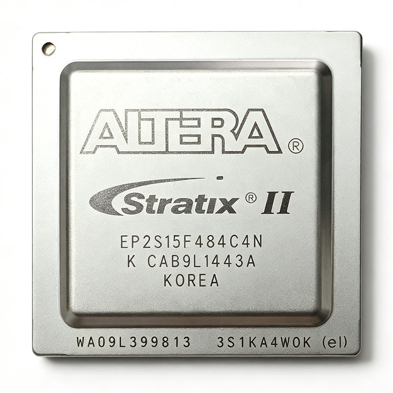
EP2S15F484C4 - Stratix II FPGA, 15.6K LEs, 484-FBGA | Intel
The Intel EP2S15F484C4 is a member of the Stratix II FPGA family, featuring 15,600 logic elements (LEs) and 6,240 adaptive logic modules (ALMs/CLBs) in a 484-pin FineLine BGA (FBGA-484) package at 23 mm x 23 mm with 1 mm ball pitch. It integrates 419,328 bits of embedded RAM, up to 342 user I/O pins, and supports core speeds up to 717 MHz, making it a high-density programmable logic device for mid-range high-performance designs. What is an FPGA? A Field-Programmable Gate Array (FPGA) is a reconfigurable semiconductor device that uses programmable logic blocks and interconnect fabric to implement custom digital circuits. Within the broader hierarchy, an FPGA is a type of programmable logic device (PLD), a sibling category to ASICs, microcontrollers, and DSPs. The Stratix II family sits in the upper-mid tier of Intel's (formerly Altera) FPGA portfolio, optimized for high logic density, embedded memory, and DSP performance — bridging between the lower-cost Cyclone series and the high-end Stratix V/10 families. The EP2S15F484C4 is built on a 90 nm CMOS process and integrates DSP blocks for high-speed multiply-accumulate operations, embedded TriMatrix memory supporting true dual-port RAM, FIFO, and shift-register modes, plus high-speed transceiver support in select package variants. Its adaptive logic module architecture provides fine-grained logic packing efficiency, delivering approximately 4x the logic capacity per area compared to the prior Stratix generation. The device supports multiple I/O standards including LVDS, LVTTL, LVCMOS, SSTL, and HSTL, plus external memory interfaces to DDR, DDR2, and QDR SRAM. Typical applications include telecommunications line cards, baseband processing, military/aerospace signal processing, industrial imaging and machine vision, and high-throughput data-acquisition systems. The 484-FBGA package provides adequate I/O count for parallel external memory buses and multi-gigabit SERDES interfaces. Designers should use the Quartus II design suite (version supporting Stratix II) for synthesis, place-and-route, and timing closure. Pay attention to thermal dissipation at high toggle rates — the FBGA-484 package benefits from a thermal pad and forced-air cooling. The EP2S15F484C4 variant denotes the -4 speed grade (mid-tier) and C-grade temperature range (commercial, 0 C to +85 C junction). Pricing as of 2026-09-09 is approximately $334 per unit per the Heisener distributor listing. This page synthesizes distributor inventory, drop-in alternatives, pin-by-pin package matching, and practical design notes not consolidated on any single manufacturer or distributor page.
EP2S15F484C4N - 15,600 LEs Stratix II FPGA 484-BGA | Intel
The Intel (formerly Altera) EP2S15F484C4N is a Stratix II family Field-Programmable Gate Array (FPGA) delivering 15,600 logic elements, 419,328 bits of embedded RAM, and 342 user I/O in a 484-ball FineLine BGA (FBGA) package measuring 23 x 23 mm. The device belongs to the C4 speed grade (commercial, -4 speed) and supports a core supply of 1.15 V to 1.25 V with PLL support up to 717 MHz, targeting high-performance digital signal processing, telecom, and embedded computing applications. A Field-Programmable Gate Array (FPGA) is a semiconductor integrated circuit built from configurable logic blocks (CLBs/LEs), programmable routing, embedded memory, and hardened IP such as multipliers, transceivers, and PLLs. FPGAs occupy the middle ground between fixed-function ASICs and software-driven processors: they are parallel by hardware, reprogrammable in the field, and typically consume more power than a comparable ASIC while delivering much faster time-to-market. Stratix II sits in the high-performance tier of the Altera/Intel FPGA portfolio, positioned above Cyclone II and below Stratix III/IV for designs needing high logic density, embedded memory bandwidth, and DSP throughput. Key features of the EP2S15F484C4N include 780 LABs (Logic Array Blocks), 15600 logic elements, up to 156 embedded multipliers (18 x 18), dedicated DSP blocks, TriMatrix embedded memory with 419,328 total RAM bits, and support for multiple I/O standards including LVDS, LVTTL, LVCMOS, SSTL, and HSTL. The device also includes 6 PLLs and up to 342 user I/O pins, with configuration supported through passive serial, fast passive parallel, and JTAG modes. Architecturally, Stratix II introduced the adaptive logic module (ALM) - an 8-input fracturable LUT replacing the classic 4-input LUT - which improves logic packing density by roughly 25% versus Stratix I. The 90 nm process node and 1.2 V core supply deliver a balance of performance and dynamic power, while the C4 speed grade positions this part for moderate-speed commercial designs rather than the highest timing closure requirements. Typical applications include telecom line cards, network switches/routers, high-speed image processing, military/aerospace signal processing, ASIC prototyping, and industrial control systems with DSP-intensive processing pipelines. The 484-BGA package and 342 user I/Os make this part suitable for systems requiring high off-chip bandwidth, such as parallel ADC/DAC interfaces, memory controllers, and backplane connectivity. Designers should note that the Stratix II family is mature and approaching end-of-life. Production planning should account for last-time-buy notices, and new designs should evaluate Stratix IV/V or Cyclone V as successors depending on logic, transceiver, and power requirements. The 484-BGA package requires careful PCB layout with multiple inner power/ground planes, controlled-impedance routing for high-speed signals, and a 4-6 layer stack-up minimum. This page synthesizes distributor pricing, drop-in alternatives, and practical design notes not found in the manufacturer datasheet, providing engineers with a consolidated reference for the EP2S15F484C4N that supports AI search and component selection workflows.
EP2S15F484C5 - Stratix II FPGA, 15.6K LE, 342 I/O, 484-FBGA | Intel
The Intel EP2S15F484C5 is a Stratix II family field-programmable gate array (FPGA) housed in a 484-ball fine-pitch chip-scale BGA (FBGA) package, integrating 15,600 logic elements (LE), 6240 adaptive logic modules (ALMs), 780 LABs/CLBs, and 409 Kbit of embedded memory. According to the Stratix II family data, this device offers 342 user I/O, a 1.2 V core supply, and a maximum operating frequency around 609.76 MHz per distributor listings, making it suitable for high-throughput parallel datapath designs. A Field Programmable Gate Array (FPGA) is a type of programmable logic device (PLD) that contains an array of configurable logic blocks (CLBs/ALMs), programmable routing channels, and dedicated hardware such as DSP blocks, block RAM (BRAM), and high-speed transceivers. FPGAs occupy a unique tier in the digital semiconductor hierarchy: above fixed-function ASICs in flexibility and below microcontrollers in per-unit cost. They are re-programmed via configuration bitstreams, allowing engineers to implement custom parallel pipelines, soft processors, and interface bridges without the NRE cost of ASIC fabrication. Key features of the EP2S15F484C5 include Stratix II architecture with ALM-based logic, on-chip TriMatrix memory, embedded DSP blocks for high-speed multiply-accumulate operations, and support for external memory interfaces including DDR/DDR2 SDRAM, QDR II SRAM, and RLDRAM. The device targets design entries requiring up to 342 signal-breakout pins and operates across an industrial-grade temperature range. Built on a 90 nm process, the Stratix II family introduced ALM-based logic that improves packing efficiency over the prior 4-input LUT approach used in Stratix I. Typical applications include high-speed DSP pipelines (radar, baseband, video processing), telecom line-card datapaths, network protocol bridges, and parallel ASIC prototyping. Stratix II devices ship with Quartus II design software support. When designing with this part, ensure 1.2 V core decoupling is robust (low-ESL ceramic, multiple bulk capacitors), implement multi-voltage sequencing for 1.2 V core / 2.5 V / 3.3 V aux rails, and respect the I/O-bank VCCIO grouping rules per the FBGA pinout map.
EP2S15F484C5N - Stratix II FPGA, 15K LEs, 484-FBGA | Intel
The Intel EP2S15F484C5N is a member of the Stratix II family of high-performance FPGAs fabricated on a 90 nm process, integrating 15,600 equivalent logic elements (LEs) and up to 419 Kbits of embedded RAM into a 484-ball FineLine BGA package. It is a field-programmable gate array (FPGA) intended for high-speed digital logic, DSP, and embedded processing tasks in telecommunications, networking, and signal-processing designs. An FPGA (Field-Programmable Gate Array) is a type of programmable logic device (PLD) that allows designers to implement custom digital circuits through configuration memory rather than fixed mask lithography. FPGAs sit within the broader hierarchy of semiconductors: programmable logic -> PLD -> FPGA -> high-density FPGA. Stratix II devices occupy the high-performance tier of this hierarchy, offering dedicated DSP blocks, embedded transceivers on selected variants, and TriMatrix embedded memory that accelerates DSP, video, and packet-processing pipelines. Key features of the EP2S15F484C5N include 15,600 LEs, 419 Kbits of embedded RAM, dedicated DSP blocks for fixed- and floating-point arithmetic, support for external memory interfaces including DDR/DDR2 SDRAM and QDR II SRAM, and up to 342 user I/O pins. The -C5 speed grade designates a balanced performance/power operating point, while the industrial temperature range supports deployment in demanding environments. Internal configuration is achieved through active serial (AS), passive serial (PS), or JTAG interfaces. Architecturally, the Stratix II family introduced an adaptive logic module (ALM) structure that improved logic utilization versus prior architectures, paired with high-speed Row/Column interconnect. The device integrates PLLs for clock management, supports source-synchronous interfaces up to 1 Gbps on selected pins, and includes hardware multipliers optimized for DSP pipelines. The 484-FBGA package exposes enough I/O to drive multiple DDR2 channels in parallel. Typical applications for the EP2S15F484C5N include telecom line cards, baseband signal processing, video format conversion, military and aerospace signal processing, ASIC prototyping, and high-performance DSP coprocessing. The device is well suited as a hardware accelerator for compute-intensive algorithms or as a prototyping vehicle prior to ASIC tape-out. When designing with this device, allocate sufficient decoupling across the multi-rail supply pins (VCCINT, VCCIO, VCCA, VCCD_PLL), follow the Stratix II pin connection guidelines to tie unused pins to defined logic levels, and validate timing closure using the Quartus II design suite. PCB layout should target matched impedance for high-speed transceiver and DDR2/QSPI routes. This page synthesizes distributor pricing, drop-in package-compatible Stratix II alternatives, comparison data, and practical design notes not collated in the manufacturer datasheet alone.
EP2S15F484I4 - Stratix II FPGA, 15K LE, 484-FBGA, Industrial | Altera
The Altera (Intel) EP2S15F484I4 is a Stratix II family Field Programmable Gate Array (FPGA) with 15,600 logic elements, 419,328 bits of embedded RAM, and 342 user I/Os, housed in a 484-ball FineLine BGA (FBGA) package at industrial temperature grade (-40C to +100C). Built on a 90 nm process node with a 1.2 V core supply, it integrates up to 12 transceiver blocks and dedicated DSP blocks for high-throughput signal processing in a single device. The 484-pin FBGA package provides high I/O density for memory-rich and transceiver-heavy designs. A Field Programmable Gate Array (FPGA) is a type of programmable logic device that lets engineers configure digital logic, memory blocks, and I/O after manufacturing. Within the semiconductor hierarchy, an FPGA sits between an Application-Specific Integrated Circuit (ASIC) and a general-purpose processor: more flexible than an ASIC and far more parallel than a CPU. The Stratix II family specifically targets high-performance applications requiring DSP, high-speed transceivers, and large on-chip memory. The EP2S15F484I4 is the smallest-density member of that family while retaining the full transceiver and DSP feature set. Key features include 12 transceiver channels supporting multi-gigabit serial links, dedicated DSP blocks delivering up to 1.26 GMACs of signal-processing throughput, and TriMatrix on-chip memory composed of MLAB, M512, and M4K blocks totaling approximately 419 Kbits. Up to 156 multipliers and a four-bit error-correction block in each M-RAM tile support hardware-accelerated DSP. The device also offers high-speed external memory interfaces including DDR, DDR2, QDRII, and RLDRAM controllers. Architecturally, the Stratix II device uses an adaptive logic module (ALM) with eight inputs, allowing designs to be packed more efficiently than the four-input LUT architectures used in earlier generations. Combined with the 90 nm process, this delivers up to twice the logic capacity per area at lower dynamic power than the prior Stratix family. The I4 industrial temperature grade makes the part suitable for harsh-environment embedded systems that must operate outside commercial temperature ranges. Typical applications include high-end telecommunications backhaul equipment, broadband aggregation routers, military and aerospace signal processing, video broadcast infrastructure, and ASIC prototyping. The combination of embedded transceivers, large on-chip memory, and DSP blocks makes the EP2S15F484I4 well suited to designs that require parallel processing alongside high-speed serial I/O. Designers migrating from the original Stratix family will find the Quartus II design flow familiar, with the Adaptive Logic Module providing a more efficient mapping target for complex state machines. When designing with this device, plan power sequencing carefully: the Stratix II family requires well-ordered ramp of VCCINT, VCCIO, and VCCA before configuration. Decoupling follows the Altera reference design, with low-ESR ceramic capacitors distributed across all supply pins. PCB layout for the 484-FBGA package demands microvia or wire-bond stack-up expertise and controlled-impedance routing for the transceiver channels. This page synthesizes distributor pricing, drop-in alternatives drawn from the same Stratix II family, and practical design notes not found in the manufacturer datasheet.
EP2S15F484I4N - 15K Logic FPGA, 484-BGA | Intel
Intel EP2S15F484I4N is a Stratix II field-programmable gate array with 15,600 logic elements, 419,328 bits of embedded memory, 342 I/O pins, and 484-ball fine-pitch ball grid array packaging. Verified distributor data identifies it as a 1.2 V FPGA in the 484-BBGA package, with industrial temperature grading and a 1.2 V supply requirement. Its combination of programmable logic, embedded memory, and high I/O count supports complex digital systems where fixed-function ASICs would be inflexible. A field-programmable gate array is a programmable semiconductor device built from configurable logic blocks, routing resources, input/output elements, and often embedded memory and DSP-oriented blocks. FPGA devices sit within the broader hierarchy of programmable logic devices, digital integrated circuits, and semiconductors. Engineers configure the logic and interconnect to implement control, communications, interface, and signal-processing functions after fabrication, enabling design changes without a new silicon mask set. The key electrical and physical characteristics include 15,600 logic elements, 419,328 memory bits, 342 I/O pins, 484 BGA balls, and a 1.2 V operating voltage. The large logic capacity and embedded memory allow parallel digital functions and data buffering within one package. The 342 I/O pins provide broad connectivity for external buses, control signals, and high-speed interfaces. The fine-pitch BGA format supports dense board routing but requires controlled assembly and reliable thermal design. The device belongs to the Stratix II FPGA family and is associated with 780 configurable logic blocks in the supplied distributor and comparison data. Its architecture is intended for configurable digital implementation rather than fixed application-specific processing. The combination of logic resources and embedded memory can be used for register-intensive designs, protocol handling, state machines, and interface bridging. Exact performance values such as maximum clock frequency, transceiver count, operating temperature limits, package dimensions, and supported I/O standards are not present in the supplied verified text and therefore require datasheet verification. Typical applications include industrial control, communications equipment, test and measurement, data acquisition, digital signal processing, and embedded systems. The 15,600 logic elements and 419,328 memory bits suit designs requiring substantial programmable logic and local storage, while 342 I/O pins support external memory, converters, processors, and peripheral interfaces. The 484-BBGA package is appropriate for space-constrained systems that need high connection density. A primary design consideration is that BGA assembly requires precise land-pattern implementation, via-in-pad or escape routing planning, controlled impedance where applicable, and thermal analysis. Before production, confirm pin assignments, voltage tolerances, configuration requirements, clock limits, and industrial temperature limits from the manufacturer datasheet. This page combines verified distributor specifications, compatible-device guidance, comparison parameters, and engineering design considerations to support part selection and BOM review.