FPGA & CPLD
Products (6358)

EP3SL340F1517C2N - Stratix III L FPGA 337.5K LE 1517-FCBGA | Intel
The Intel (formerly Altera) EP3SL340F1517C2N is a high-density, low-power Stratix III L family Field Programmable Gate Array (FPGA) housed in a 1517-ball FineLine BGA (FCBGA) package. Built on a TSMC 65 nm process, it integrates 337,500 logic elements, 18,821,184 bits of embedded memory, 13,500 adaptive logic modules (ALMs/LABs), and 976 user I/O pins, and is rated for a maximum core clock frequency of 600 MHz at a 1.1 V core supply. An FPGA (Field Programmable Gate Array) is a class of programmable logic device that combines configurable logic blocks, programmable interconnects, and dedicated hardware resources such as block RAM, DSP blocks, PLLs, and high-speed transceivers. FPGAs sit in the hierarchy of programmable logic devices (PLD) alongside CPLDs and are the densest members, used to implement custom parallel datapaths, protocol bridges, signal-processing pipelines, and ASIC prototyping. The Stratix III L sub-family is the lower-static-power variant of Stratix III, optimized for power-sensitive applications without sacrificing logic density or DSP capability. Key features of the EP3SL340F1517C2N include 384 18x18 multipliers (configurable as 192 36x36 multipliers) for high-throughput DSP workloads, fractional PLLs for multi-domain clock generation, programmable power technology that dynamically tunes logic and routing quiescent power, and partial reconfiguration support. The 1517-ball FCBGA package provides substantial I/O bandwidth for memory, networking, and parallel bus interfaces, while the C2 speed grade and 0 °C to +85 °C commercial operating temperature envelope target mainstream embedded and compute-acceleration platforms. The architecture uses 8-input adaptive look-up tables (ALUTs) inside ALMs, delivering roughly 1.4x the logic capacity of a comparable Stratix II design at lower power. Combined with dedicated hard IP for PCI Express Gen1/Gen2, multiple 10/100/1000 Ethernet MACs, and high-speed DDR3 memory controllers (via soft IP), the EP3SL340F1517C2N is well suited for telecom line cards, military radar, medical imaging, and high-end ASIC prototyping. Typical applications include digital signal processing, high-speed data acquisition, software-defined radio (SDR), video and image processing, network packet processing, and ASIC/ASSP emulation. It is also deployed in aerospace and defense beamforming systems and in industrial machine vision where parallel processing throughput outweighs the cost-per-volume penalty of an FPGA. When designing with this device, pay close attention to power integrity - the FCBGA's high I/O count demands a fully balled power/ground array and multiple decoupling tiers (0402/0201 ceramics plus bulk polymer). Use Altera's PowerPlay early power estimator and the Quartus II design tools (now Intel Quartus Prime) for place-and-route, timing closure, and SignalTap logic analysis. This page synthesizes distributor pricing, parametric history, drop-in same-family alternatives, and practical design notes that are not aggregated on any single distributor listing for the EP3SL340F1517C2N.
EP3SL340F1517C3 - 337,500-Cell FPGA | Intel | Digital Logic
Intel EP3SL340F1517C3 is a high-density Stratix III L FPGA built for programmable digital systems requiring substantial logic capacity and extensive external interfacing. Its verified headline parameters are 337,500 logic cells, 976 user I/O pins, and 13,500 LABs, housed in a 1517-ball FCBGA package. This combination places the device in the FPGA and CPLD category while supporting designs that need many parallel interfaces, custom datapaths, and reconfigurable processing logic. An FPGA, or field-programmable gate array, is a semiconductor device containing programmable logic blocks, routing resources, memory elements, and configurable I/O. Engineers configure these resources to implement digital functions after manufacturing. In the system hierarchy, EP3SL340F1517C3 belongs to FPGA devices, programmable logic, digital integrated circuits, and ultimately semiconductors. Unlike a fixed-function ASIC, the FPGA can be revised through configuration data without changing the silicon device. The verified 337,500-cell capacity supports large control engines, interface aggregation, and custom high-speed digital functions. The device provides 976 I/O pins for connecting numerous peripheral buses, memory interfaces, converters, and control signals. Its 13,500 LABs provide a broad fabric for implementing combinational and sequential logic. The 1517-pin FCBGA package offers high interconnection density but requires advanced PCB design, controlled impedance routing, reliable power distribution, and careful thermal management. The part is identified as a 65 nm Stratix III L device with a 500 MHz specification reported by the supplied FPGAkey result and a 1.1 V core-voltage value also reported there. Another distributor result describes 18,822,144 bits and 337,500 logic elements/cells. These values establish a large programmable architecture, but detailed timing, transceiver count, memory capacity, operating temperature, and package dimensions remain subject to the manufacturer datasheet. The configuration interface, supported I/O standards, embedded resources, and exact speed grade must be confirmed before release to production. Typical applications include communications equipment, industrial automation, test and measurement, video and imaging systems, and high-channel-count data acquisition. In these systems, the FPGA can consolidate control logic, protocol conversion, parallel data processing, and timing functions into one programmable platform. The 976 I/O count is particularly useful where many external devices or parallel buses must be connected. Designers should treat the FCBGA as a high-density system-in-package challenge rather than a conventional low-pin-count IC. Validate the complete Intel pin assignment, power-up sequence, decoupling network, signal-integrity constraints, and thermal solution from the manufacturer documentation. A board redesign is normally required when moving to another FPGA family, density, package, or pinout. This data set combines verified distributor specifications, package information, indicative commercial data, and clearly marked engineering gaps. It is intended to support early component selection, sourcing research, and architecture planning, not to replace the manufacturer datasheet, qualification records, or final signal-integrity and thermal analysis.

EP3SL340F1517C3N - Stratix III L FPGA, 337.5K LE, 1517-FCBGA | Altera
The Altera (now Intel) EP3SL340F1517C3N is a high-density Stratix III L Field Programmable Gate Array built on a 65 nm low-power CMOS process, delivering 337,500 logic elements and 18,822,144 bits of embedded memory in a 1517-ball FC-BGA package. The -3N speed grade targets clock frequencies up to 500 MHz, with 1.1 V core supply, commercial 0C to 85C temperature range, and 976 user I/O pins. It is the lowest-power member of the Stratix III family, optimized for high-performance DSP, telecommunications, and ASIC-prototype applications. An FPGA (Field Programmable Gate Array) is a programmable logic device containing configurable logic blocks (LABs), embedded memory, DSP blocks, and routing resources that the designer wires up using a hardware description language. FPGAs sit in the wider taxonomy as programmable logic devices → semiconductor ICs → integrated circuits, and offer ASIC-like performance with NRE-free, fast-turn development. The Stratix III family uses Altera's adaptive logic module (ALM) architecture, which folds 8-input fracturable look-up tables into a flexible logic element that improves effective density and reduces dynamic power versus prior Stratix generations. Key features include 337,500 logic elements organized into 13,500 LABs, 18.8 Mbits of embedded RAM (triple-port M9K and M144K blocks), dedicated DSP blocks for high-throughput multiplication-accumulation, up to 24 transceivers (speed grade and package dependent) for multi-gigabit serial I/O, and hard memory controllers. The 1517-ball FC-BGA package supports the highest I/O count and richest transceiver density in the Stratix III L family, and integrates a serial digital temperature-sensing diode for on-board thermal management. The -3N speed grade balances timing margin and Fmax (industry-standard notation where lower speed-grade numbers are slower, higher numbers faster); -3 is the fastest commercial grade in Stratix III L, and the N suffix denotes lead-free / RoHS-compliant ball metallurgy. Combined with 1.1 V core, it allows significant static and dynamic power reductions compared with Stratix II, while preserving the transceiver bandwidth and DSP throughput needed for baseband processing, video pipeline, and high-speed bridging. Typical applications include wireline telecom line cards, software-defined radio (SDR), ASIC prototyping, broadcast video processing, and high-performance DSP coprocessors. The dense embedded memory and wide datapath make the EP3SL340F1517C3N well suited to packet buffering and FEC (forward error correction) in 100G-class networking platforms, as well as medical-imaging reconstruction engines and radar signal pre-processing. When designing with this part, pay close attention to PCB stack-up and power-tree planning: the 1517-ball FC-BGA requires microvia or via-in-pad technology, the core and I/O banks each need their own decoupling strategy, and Quartus II (or newer Intel Quartus Prime) power analysis should be run early to size the switching regulator for the dynamic load profile. Transceiver channels must be routed with controlled-impedance differential pairs and length-matched within the budget defined by the protocol (PCIe, Serial RapidIO, CEI-6G, etc.). This page synthesizes Stratix III L distributor pricing, same-package alternatives, and PCB-level design notes that go beyond the device datasheet and Quartus II device handbook content.
EP3SL340F1517C4 - Stratix III L FPGA 337.5K LE 1517-FCBGA | Intel
The Intel (formerly Altera) EP3SL340F1517C4 is a high-density Stratix III L Field Programmable Gate Array (FPGA) integrating 337,500 logic elements (LE), 18,822,144 bits of embedded memory, and 976 user I/Os into a 1517-ball FineLine BGA (FCBGA) package. Built on TSMC's 65 nm process and built around an adaptive logic module (ALM) fabric, this part is rated for 500 MHz core operation and targets the highest-density, I/O-rich system-on-chip designs of its generation. An FPGA (Field Programmable Gate Array) is a programmable semiconductor whose logic fabric and interconnect can be reconfigured by the customer after manufacture, sitting in the hierarchy between ASICs (full custom, fixed) and CPLDs (smaller, non-volatile). Stratix III L devices were positioned by Intel/Altera for high-throughput DSP, high-speed serial interconnect, and high-bandwidth memory-interface designs, occupying the upper tier of the FPGA taxonomy below Stratix IV/V and above Cyclone series devices. Key features include 13,500 Logic Array Blocks (LABs), 18,822,144 embedded RAM bits distributed across TriMatrix memory blocks, 500 MHz internal fabric frequency, 800 MHz maximum internal frequency, 976 user I/O pins, and a 1.1 V core supply. The 1517-FCBGA (FCBGA, 40x40 mm class substrate) is the largest package in the Stratix III L family and supports the device's full I/O count including multiple high-speed transceiver banks. Architecturally the EP3SL340F1517C4 leverages the ALM-based logic fabric introduced in Stratix III, allowing 8-input fracturable look-up tables with arithmetic mode and a MultiTrack interconnect for predictable timing closure. The TriMatrix memory subsystem provides three distinct block RAM depths (640-bit MLAB, 9-Kbit M9K, 144-Kbit M144K) tuned to different DSP and buffering use cases. Typical applications include high-speed networking line cards, ASIC prototyping, software-defined radio baseband processing, high-end DSP co-processing, and digital video broadcast infrastructure. The combination of 337.5K LE and 976 user I/Os makes the part appropriate for bridging multiple external memory channels and parallel high-speed data converters. When designing with this device, ensure the PCB has sufficient BGA breakout fan-out, a controlled-impedance stack-up for the high-speed I/Os, and a multi-rail power delivery network that matches Stratix III PowerPlay recommendations. Octopart currently lists 14 active distributors for this MPN. This page synthesizes distributor pricing, drop-in same-package alternatives from the Stratix III/IV L families, and practical design considerations not consolidated on any single distributor page.
EP3SL340F1517C4L - Stratix III L FPGA, 337K LEs, 1517-FCBGA | Intel
The Intel (formerly Altera) EP3SL340F1517C4L is a high-density, low-power member of the Stratix III L FPGA family, delivering 337,500 logic elements (LEs), 18,822,144 bits of embedded memory, and 976 user I/Os in a 1517-ball FineLine BGA (FCBGA) package. The trailing 'L' denotes the Stratix III L sub-family optimized for the lowest static power at performance parity with Stratix III E. The 'C4' speed grade and 'L' suffix indicate commercial temperature grade (0 °C to +85 °C), Pb-free/RoHS-compliant assembly. A Field-Programmable Gate Array (FPGA) is a programmable logic device whose function is defined by customer-written configuration data after manufacture. The Stratix III architecture places it within the broader hierarchy: programmable logic -> FPGA -> high-performance FPGA with embedded transceivers and DSP blocks -> 65-nm low-power node -> complex system-on-chip platform. Designers use FPGAs when ASIC NRE costs cannot be amortized, when time-to-market dominates, or when in-system reprogrammability is required. Key specifications include up to 1.4 Gbps LVDS performance, dedicated 9-bit DSP blocks for high-throughput arithmetic, 18x18 multipliers, embedded memory blocks up to 1,152 Kbits per block, and 12 PLLs for clock synthesis. The 1517-FCBGA package provides sufficient I/O density for parallel interface buses, memory controllers, and high-speed serial aggregation in a single device. The 65-nm process node and proprietary logic structure yield a typical static power reduction versus the Stratix III E variant. The architecture supports up to 12.5 Gbps transceivers (where applicable in E variants), hard PCI Express and external memory controllers, and partial reconfiguration for power-managed systems. The device integrates 4 hard memory controllers and 8 PLLs standard. Typical applications include high-end telecommunications line cards, ASIC prototyping, broadcast video processing, military signal processing, and high-performance computing accelerators. Designers benefit when 337K LEs of logic capacity and 18 Mbits of memory are required within a single low-power device. When designing with this FPGA, confirm PCB footprint compatibility with the 1517-ball 1.0 mm pitch FCBGA land pattern. Use the Altera Quartus II or Intel Quartus Prime design suite; older versions are required because Stratix III is in maintenance status. Provide adequate decoupling on all VCC/VCCPD/PWR rails. This page synthesizes distributor pricing, drop-in alternatives, and practical design notes not found in the standalone manufacturer datasheet, giving engineers a consolidated reference for sourcing, replacement, and selection decisions.
EP3SL340F1517C4LN - Stratix III L FPGA, 337.5K LE, 1517-FBGA | Intel
The Intel EP3SL340F1517C4LN is a high-density, low-power Stratix III L Field Programmable Gate Array (FPGA) with 337,500 logic elements, 18,822,144 bits of embedded memory, and 976 maximum user I/Os, housed in a 1517-pin FC-FBGA (Flip-Chip Fine-pitch Ball Grid Array) package. It is fabricated on a 65 nm CMOS process with a 1.1 V core supply, operates at up to 450 MHz fabric performance, and ships in the commercial 0C to 85C temperature grade with Pb-free lead finish. A Field Programmable Gate Array (FPGA) is a semiconductor device whose digital logic, interconnect, and I/O behavior are defined by user-supplied configuration data rather than by hard-wired mask geometry. Within the broader programmable logic hierarchy, FPGAs sit above CPLDs in density and below ASICs in unit cost; the Stratix III family is Intel's high-performance, low-power FPGA line targeting ASIC prototyping, DSP, and high-speed serial I/O. The 'L' variant (Stratix III L) emphasizes lower static and dynamic power versus the standard Stratix III E family, while preserving the same architecture. Key specifications of the EP3SL340F1517C4LN include up to 13,500 Logic Array Blocks (LABs), embedded DSP blocks for high-throughput arithmetic, up to 24 transceivers on selected package variants, and rich clock management with PLLs. The 1517-BBGA package provides the largest I/O count in the Stratix III L family and supports high-speed memory interfaces such as DDR3 and QDR II+ with dedicated DQS/DQ pins. Configuration is supported via fast passive parallel, fast active serial, or JTAG. Architecturally, the device combines Adaptive Logic Modules (ALMs) for fine-grained logic, TriMatrix embedded memory blocks of three depths (MLAB, M9K, M144K) for flexible buffering, and dedicated 18x18 multipliers for DSP. The Quartus II design suite is the primary toolchain. Compared to gate-array ASICs at this density, the EP3SL340F1517C4LN offers in-system reprogrammability and immediate prototyping turnaround at the cost of higher per-unit price and lower raw clock frequency. Typical applications include high-end ASIC prototyping, wireline telecom line cards, high-performance DSP for radar and medical imaging, broadcast video processing, and military/aerospace test systems. Its 976 user I/Os make it suitable for memory-intensive designs requiring wide external buses, while the 65 nm process keeps dynamic power manageable for thermally constrained chassis designs. When designing with this FPGA, engineers should plan power sequencing for the 1.1 V core, 2.5 V/3.3 V auxiliaries, and PLL analog supplies separately, and allocate sufficient PCB area for the 1517-ball FC-FBGA footprint. Thermal management is critical: a heatsink with controlled airflow is typically required for continuous operation at full fabric utilization. This page synthesizes distributor pricing, drop-in Stratix III L alternatives, and practical design notes not found on a single manufacturer page.
EP3SL340F1517C4N - Stratix III L FPGA 337K LE | 1517-FCBGA
The Intel (formerly Altera) EP3SL340F1517C4N is a high-density, low-power Stratix III L family Field Programmable Gate Array (FPGA) IC built on a 65 nm process, providing 337,500 logic elements, 18,822,144 bits of embedded memory, and 976 user I/Os in a 1517-ball FC-BGA package. The "L" variant of Stratix III delivers the lowest static power in the family while preserving the high-performance fabric architecture that established Stratix III as a benchmark in DSP and transceiver-based designs. A Field Programmable Gate Array (FPGA) is a semiconductor integrated circuit composed of configurable logic blocks (CLBs), programmable interconnect, and dedicated hard IP such as transceivers, memory blocks, and DSP slices. Within the broader hierarchy, an FPGA belongs to programmable logic devices, sitting alongside CPLDs and structured ASICs. Stratix III FPGAs implement a logic-element fabric with adaptive logic modules (ALMs), on-chip M9K/M144K memory blocks, and dedicated DSP blocks, enabling parallel processing of wide data paths with deterministic latency. Key features of the EP3SL340F1517C4N include 13,500 LABs, up to 450 MHz fabric performance, support for multiple I/O standards (LVDS, LVTTL, LVCMOS, HSTL, SSTL, PCIe), embedded transceivers at multi-gigabit data rates, and a 1.1 V core supply. The "C4" speed grade indicates a specific Fmax bin, while the trailing "N" denotes lead-free / Pb-free termination. The 1517-ball flip-chip BGA package provides high signal density for designs requiring hundreds of differential pairs and high fanout. Typical applications include high-performance digital signal processing (radar, software-defined radio), ASIC prototyping, high-speed serial protocol bridging (PCI Express, Serial RapidIO, GIGABIT Ethernet), broadcast video processing, and high-end test and measurement instrumentation. The combination of 18.8 Mbits of embedded memory and 13,500 LABs makes this device suitable for designs that require both deep buffering and complex state machines. When designing with this part, ensure your PCB BGA layout supports 1.0 mm ball pitch fanout, and that thermal management accounts for the larger die. Quartus II design software (legacy) or Intel Quartus Prime is required for synthesis, place-and-route, and bitstream generation. Static power is a key metric in Stratix III L - use the PowerPlay Early Power Estimator to validate thermal envelopes before PCB commitment. This page synthesizes distributor stock levels, drop-in package-compatible alternatives from the Stratix III / Stratix III L / Stratix IV families, and practical PCB thermal guidance not consolidated in any single manufacturer or distributor page.
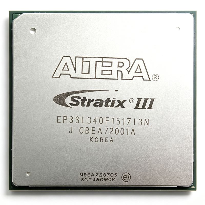
EP3SL340F1517I3 - Stratix III L FPGA, 337500 LEs, 1517-FBGA | Intel
The Intel EP3SL340F1517I3 is a high-density Stratix III L family Field Programmable Gate Array (FPGA) delivering 337,500 logic elements, 18,822,144 bits of embedded memory, and 976 user I/O pins in a 1517-ball flip-chip BGA (FC-FBGA) package. Built on TSMC's 65 nm process and running from a 1.1 V core supply, this FPGA targets the lowest-power, highest-performance tier of the Stratix III generation and is specified for the industrial temperature range of -40C to +100C. An FPGA (Field-Programmable Gate Array) is a semiconductor device built around a matrix of configurable logic blocks (CLBs), dedicated DSP blocks, embedded memory blocks, and high-speed serial transceivers, all interconnected by a programmable routing fabric. Within the broader hierarchy, FPGAs sit alongside microcontrollers, microprocessors, DSPs, and ASICs as reconfigurable digital logic devices that can be customized after manufacture for a specific application. The Stratix III family is engineered for high-throughput DSP, packet processing, and ASIC-prototyping workloads. Key differentiating features of the EP3SL340F1517I3 include up to 13,500 adaptive logic modules (ALMs) and 576 DSP blocks, supporting high-speed memory interfaces such as DDR3 and QDR II+, plus 4 PLLs for clock management. The device includes 976 user I/O pins distributed across 24 I/O banks, supporting a wide range of single-ended and differential I/O standards (LVDS, LVTTL, LVCMOS, SSTL, HSTL) for board-level flexibility. Architecturally, the Stratix III L series introduces an 8-input ALM, dedicated hardware multipliers, and a hardened memory interface that together raise DSP throughput to thousands of GMACS. The 65 nm process node and 1.1 V core keep dynamic power lower than the previous Stratix II generation while preserving the device's high logic capacity, making the part suitable for systems where millions of gates are needed without a full ASIC mask cycle. Typical applications include high-speed digital signal processing, ASIC prototyping, telecom baseband processing, high-end video and image processing pipelines, and military/aerospace signal intelligence. The 1517-BGA package provides ample I/O for memory-rich designs. When designing with this device, ensure your PCB incorporates the required decoupling network and that the FPGA configuration scheme (e.g., AS, PS, JTAG) is selected correctly. Use the Altera Quartus II toolchain for synthesis, place-and-route, and timing closure. This page synthesizes distributor pricing, same-family Stratix III drop-in alternatives, and practical FPGA design notes not consolidated on any single distributor or manufacturer page.
EP3SL340F1517I3N - Stratix III L FPGA, 337.5K LE, 1517-BGA | Intel
The Intel (Altera) EP3SL340F1517I3N is a high-density Stratix III L family Field Programmable Gate Array (FPGA) built on a 65 nm low-power process, delivering 337500 logic elements (337.5K LE) and 18822144 bits (approximately 18 Mbit) of embedded memory in a 1517-ball FCBGA package. The device integrates 976 user I/O pins, 24 transceiver channels at up to 8.5 Gbps, and 1.1 V core supply, targeting high-performance DSP, memory-rich datapath, and high-bandwidth serial-interface designs. An FPGA (Field Programmable Gate Array) is a class of programmable logic device that lets engineers implement arbitrary digital logic, soft processors, and high-speed serial interfaces in silicon after fabrication. Within the broader programmable logic taxonomy (CPLD -> FPGA -> SoC FPGA), Stratix III L sits at the top of the high-performance, low-power segment, providing dedicated DSP blocks, MLABs, and embedded transceiver physical layers that are not available in CPLDs or smaller FPGAs. FPGAs belong to the digital IC family and to the embedded processing hierarchy alongside MCUs, DSPs, and ASICs. Key features of the EP3SL340F1517I3N include 13.5K adaptive logic modules (ALMs) organized into LABs, support for DDR3/QDRII+/RLDRAM II external memory interfaces, 24 full-duplex transceivers supporting PCIe Gen1/Gen2, Serial RapidIO, and 10 Gigabit Ethernet protocols, dynamic on-chip termination, programmable output drive strength, and 6.4 Gbps LVDS support. The device also offers bitstream encryption and JTAG-based configuration with multi-device support for parallel configuration of up to four devices in a chain. Architecturally, the Stratix III L uses an enhanced ALM structure (8-input fracturable LUTs with dedicated carry chains and register files), allowing higher logic density per LE than the prior Stratix II generation. The transceiver tiles are arranged in groups of six with shared clocking, providing deterministic latency and skew control for serial protocols. Power optimization features such as programmable power technology and per-block clock gating enable lower dynamic power consumption than the earlier Stratix II family at equivalent performance. Typical applications include 40G/100G wire-speed packet processing line cards, military radar baseband processing, high-end medical imaging front-end pipelines, ASIC prototyping emulators, and high-speed test-and-measurement instrumentation. The combination of 18 Mbit embedded memory, 976 user I/Os, and 24 high-speed transceivers also makes this FPGA a common choice for high-density channelized signal processing designs where multiple ADCs/DACs must be aggregated. When designing with this device, plan the PCB stack-up for the 1517-ball FCBGA carefully: the 1.0 mm ball pitch requires microvia technology and a 6+ layer stack-up to escape the high I/O count. Power plane decoupling must follow Altera's PowerPlay recommended network, with multiple bulk, mid-frequency, and high-frequency ceramic capacitors placed within the package footprint. This page consolidates distributor pricing, parametric cross-references against same-package Stratix III family members, and practical design guidance that complements the official Stratix III device handbook.
EP3SL340F1517I4 - Stratix III L FPGA, 337.5K LE, 1517-FBGA | Altera
The Altera (Intel) EP3SL340F1517I4 is a high-density Stratix III L Field-Programmable Gate Array (FPGA) IC, offering 337,500 logic elements, 18,822,144 bits of embedded memory, and 976 user I/O pins, all packaged in a 1517-ball FineLine BGA (FBGA). It is built on TSMC's 40 nm low-power process and targets high-performance logic, DSP, and memory-intensive applications where large on-chip bandwidth and high transponder counts are required. Background - what is an FPGA? A Field-Programmable Gate Array is a programmable logic device whose logic blocks, routing fabric, I/O cells, and on-die memory can be reconfigured after manufacture to implement arbitrary digital functions. FPGAs sit at the top of the programmable-logic hierarchy: ASIC < CPLD < FPGA (high-density) < SoC FPGA. Modern high-end FPGAs like the Stratix III L integrate hard IP for transceivers, DSP blocks, block RAM, and PCIe endpoints, bridging the gap between ASIC efficiency and programmable flexibility. Key features include 337,500 logic elements (LEs), 18,822,144 bits (approximately 2.25 MB) of embedded memory, 976 maximum user I/O pins, integrated DSP blocks, and dedicated memory interface blocks that support external DDR3/QDRII+ memories at hundreds of MHz. Industrial temperature grade (-40 C to +100 C) is indicated by the 'I' suffix, and speed grade 4 is one of the fastest Stratix III device speed bins offered. The 1517-BBGA package uses flip-chip BGA construction with controlled-impedance traces, supporting high-speed serial transceivers up to several Gbps. Architecturally, the Stratix III L device uses an adaptive logic module (ALM) structure that combines LUT and register resources into a single 8-input fracturable element, delivering higher effective logic density than previous-generation ALMs. This ALM plus the high transceiver count make the EP3SL340F1517I4 a strong fit for wireline backplane aggregation, broadcast video processing, and high-channel-count DSP pipelines. Typical applications include high-end telecommunications line cards, ASIC prototyping, signal-processing baseband cards, test & measurement instrumentation, and military/aerospace image processing. The 976 user I/O and the large embedded memory also suit memory-intensive compute fabrics. When designing with the EP3SL340F1517I4, plan PCB layout for the 1517-ball BGA with microvia stack-ups, follow the Quartus II power guidelines to estimate thermal dissipation, and respect the bank's VCCIO and VREF rules when mixing I/O standards. Most Stratix III designs are developed with Altera's Quartus II design suite (legacy 13.0 or earlier), since newer Quartus releases no longer include Stratix III device support. This page synthesizes distributor pricing, drop-in alternatives, and design considerations not found in the standalone manufacturer datasheet.
EP3SL340F1517I4L - 337500-Cell Stratix III L FPGA | Intel
The Intel EP3SL340F1517I4L is a high-density Stratix III L Field Programmable Gate Array (FPGA) delivering 337,500 logic elements, 18,822,144 bits of embedded memory, and 976 user I/Os, packaged in a 1517-ball FineLine BGA with a 40 mm x 40 mm body. It operates at up to 717 MHz core frequency and is fabricated on a TSMC 65 nm CMOS process, targeting high-end ASIC prototyping, high-throughput signal processing, and telecommunication infrastructure. The device ships in the -I4L industrial speed grade and is part of Intel's long-running Stratix III FPGA family, originally launched by Altera in 2006. An FPGA (Field Programmable Gate Array) is a programmable semiconductor device that allows hardware designers to implement custom digital logic circuits after manufacturing. FPGAs combine configurable logic blocks (CLBs), programmable interconnects, dedicated DSP slices, embedded memory (BRAM/M9K/M144K), high-speed transceivers, and clock management circuitry on a single die. Within the broader semiconductor taxonomy, FPGAs sit between general-purpose microcontrollers and fixed-function ASICs: more flexible than ASICs, far more parallel than CPUs, and far faster than software-only solutions for parallel DSP and packet-processing workloads. Key features of the EP3SL340F1517I4L include 13,500 LABs (Logic Array Blocks), 576 embedded 18x18 multipliers (DSP blocks), 4 PLLs, and support for external memory interfaces including DDR3, DDR2, QDR II+, and RLDRAM II. The device integrates 24 transceivers capable of up to 6.375 Gbps operation, which is the differentiator between the Stratix III L (low-power) and Stratix III GX variants. The 1517-BGA package supports 976 user I/Os - among the highest I/O count in the Stratix III family - and is appropriate for systems requiring wide external memory buses, parallel ASIC-emulation interfaces, or many LVDS channels. Architecturally, the EP3SL340F1517I4L uses a 65 nm low-k dielectric process, multi-level copper interconnect, and an adaptive logic module (ALM) based on 8-input fracturable look-up tables, which gives finer-grained logic packing and shorter critical paths than the older 4-input LUT architecture used in Stratix II. The transceivers use a hardened PCS/PMA pipeline that supports protocols such as PCIe Gen1/Gen2, Serial RapidIO, XAUI, and CEI-6G. Typical applications include wireline telecommunication line cards, software-defined radio (SDR) baseband processing, ASIC prototyping and emulation, high-performance computing (HPC) acceleration, broadcast video processing, and military/aerospace signal processing. The device is well-suited to designs that require the largest logic capacity and widest memory bandwidth in the Strat III L family. When designing with this device, engineers should carefully manage power and thermal envelopes - even the L (low-power) variant of a 337k-LE FPGA can dissipate tens of watts under heavy transceiver and DSP utilization, requiring a multi-layer PCB with continuous ground and power planes, controlled-impedance routing for the 6 Gbps transceivers, and a substantial heatsink. Industrial-grade temperature range (-40C to +100C junction) is supported by the I4 speed grade. This page synthesizes distributor pricing, drop-in same-brand and cross-brand alternatives, and practical design considerations beyond what the manufacturer datasheet alone provides, helping procurement and FPGA hardware engineers source the part more efficiently.
EP3SL340F1517I4LN - Stratix III L FPGA 337K Cells 1517-FCBGA | Intel
The Intel (formerly Altera) EP3SL340F1517I4LN is a high-density Stratix III L Field-Programmable Gate Array (FPGA) with 337,500 logic elements, fabricated on a 65 nm process node with a 0.9 V core voltage, housed in a 1517-ball FC-FBGA package with 976 user I/Os. It belongs to the Stratix III low-power (L) variant family, which combines high logic density with a reduced static power envelope compared to the standard Stratix III. An FPGA (Field-Programmable Gate Array) is a type of programmable logic device that allows hardware designers to configure digital logic blocks and interconnects after manufacturing. FPGAs sit in the broader taxonomy of programmable logic -> logic semiconductor -> integrated circuit. Unlike ASICs, FPGAs can be reconfigured in-system, enabling rapid prototyping, hardware acceleration, and low-volume custom silicon replacement. Key features include 337,500 logic elements, 18,822,144 bits of embedded memory, 13,500 LABs (Logic Array Blocks), 384 embedded 18x18 multipliers, integrated high-speed transceivers, and 976 user I/O pins. The device supports up to 8 PLLs and includes hard memory controller blocks, supporting DDR/DDR2/DDR3 external memory interfaces. The 1517-FCBGA package provides high I/O count with multi-row ball array on a 40x40 mm substrate. Architecturally, the Stratix III L FPGA uses Altera's adaptive logic module (ALM) with 8-input fracturable look-up tables (LUTs), delivering higher effective logic density than the previous Stratix II generation. The device supports hot-socketing, allowing insertion into a live backplane without damage, and offers multiple temperature grades (commercial, industrial, military) with the I4 industrial speed grade targeting -40C to +100C operation. Typical applications include high-performance digital signal processing, telecom baseband processing, ASIC prototyping, high-speed serial protocol bridging (PCIe, Serial RapidIO, Gbps Ethernet), video processing and broadcast equipment, and military/aerospace signal processing. The Stratix III L family was Altera's mainstream high-density FPGA family before being superseded by Stratix IV and Stratix V. Design consideration: Stratix III FPGAs require Quartus II design software (legacy, EOL replaced by Quartus Prime with limited Stratix III support). Power estimation requires the Playback Power Analyzer tool, and PCB designers must follow Intel's flip-chip BGA layout guidelines including microvia stack-up and 1.0 mm pitch escape routing.

EP3SL340F1760C2 - Stratix III L FPGA 337K LE | Intel | 1760-BGA
The Intel (formerly Altera) EP3SL340F1760C2 is a high-density Stratix III L-series Field Programmable Gate Array (FPGA) featuring 337,500 logic elements, 18,822,144 bits of embedded memory, and 1,120 user I/Os, housed in a 1760-ball FineLine BGA (FCBGA) package. This device targets high-throughput DSP, communications infrastructure, and ASIC prototyping designs that demand maximum logic density and rich memory/serDes resources. An FPGA (Field Programmable Gate Array) is a semiconductor integrated circuit composed of configurable logic blocks (CLBs), programmable interconnects, and dedicated hard IP blocks such as block RAM, DSP slices, transceivers, and PLLs. FPGAs belong to the broader category of programmable logic devices (PLDs), sitting alongside CPLDs in the digital logic hierarchy. Unlike fixed-function ASICs, FPGAs are reconfigured at runtime via SRAM-based configuration cells, enabling iterative design, in-system updates, and hardware acceleration for compute-bound workloads. Key features of the EP3SL340F1760C2 include 13,500 LABs (Logic Array Blocks), 1120 general-purpose I/Os, embedded Multipliers and DSP blocks for high-performance arithmetic, dedicated memory controllers, and high-speed serial transceivers. The 1760-ball FCBGA package uses Altera's FineLine BGA technology to deliver 1,120 user I/Os at a 1.0 mm ball pitch, supporting large pin-count designs that would otherwise require multi-chip partitioning. The Stratix III architecture combines a 40 nm process node with Altera's adaptive logic module (ALM) structure, doubling register density per LAB versus prior generations. Programmable Power Technology allows unused logic and routing to be powered down, reducing static power by up to 50% compared to fixed-power predecessors. Embedded PCI Express hard IP blocks and up to 48 transceivers running at 6.375 Gbps make the part suitable for high-bandwidth backplane and line-card applications. Typical applications include 40G/100G optical transport line cards, LTE baseband processing, radar and electronic warfare DSP pipelines, high-performance ASIC prototyping, and high-channel-count test and measurement instrumentation. The combination of large memory (18.8 Mbits), abundant DSP blocks, and high I/O count positions this part for designs that previously required multiple mid-range FPGAs. When designing with the EP3SL340F1760C2, careful attention must be paid to PCB layout for the FCBGA-1760 package: 1.0 mm ball pitch requires microvia stack-up, controlled-impedance routing for transceiver channels, and substantial power-plane coverage for the multi-rail core (0.9V/1.1V/1.5V/2.5V/3.3V). Designers should also budget configuration memory and select appropriate configuration schemes (e.g., fast passive parallel, JTAG) per design security and boot time requirements. This page synthesizes distributor pricing, drop-in alternatives drawn from the Stratix III/IV family, and practical design notes not found in the manufacturer datasheet alone.
EP3SL340F1760C3 - Stratix III L FPGA, 337500 Cells, 1760-FBGA | Intel
The Intel (formerly Altera) EP3SL340F1760C3 is a high-density, low-power member of the Stratix III L FPGA family, integrating 337,500 logic elements, 18,822,144 bits of embedded memory, and 1120 user I/O in a 1760-ball FC-FBGA package. Built on a 65 nm CMOS process with a 1.1 V core voltage, the device supports logic speeds up to 717 MHz and is intended for high-throughput, logic-rich designs in communications, DSP, and signal-processing subsystems. The part ships in the commercial temperature grade (-C speed grade 3), making it suitable for prototype builds and non-extended-temperature deployments. A field-programmable gate array (FPGA) is a programmable logic device that lets engineers implement arbitrary digital logic, memory, and DSP functions in silicon after fabrication. FPGAs sit above fixed-function ASICs in design flexibility and below microprocessors in programmability granularity, occupying a unique role in parallel processing pipelines. Within the Stratix III L sub-family, the 'L' suffix denotes the lower-static-power variant, optimized for power-sensitive applications while preserving the high-performance adaptive logic module (ALM) fabric. Stratix III devices support transceiver rates up to 6.375 Gbps, embedded transceivers, and hard IP for PCI Express Gen1/Gen2, depending on the die variant. Key features include 337,500 logic elements, 18,822,144 RAM bits distributed across TriMatrix memory blocks, 1120 general-purpose I/O, integrated DSP blocks with up to 224 GMACs of throughput, and a high-speed serial interface supporting multi-gigabit transceivers. The 1760-pin FC-FBGA package provides ample signal headroom for parallel buses and memory interfaces common in image processing and telecom line-card designs. Industrial design tools such as Intel Quartus Prime provide synthesis, place-and-route, and timing closure for the device, with pre-verified IP cores available for DDR2/DDR3 memory controllers, PCIe, and Ethernet MACs. Architecturally, the EP3SL340F1760C3 employs a logic-array block (LAB) structure composed of adaptive logic modules (ALMs) with eight inputs and dedicated carry chains for arithmetic operations. The 65 nm process node balances leakage and dynamic power, while the 'L' designation specifically targets reduced static power consumption. The device integrates PLLs, high-speed serial interface channels, and dedicated hardware multipliers for DSP, simplifying complex SoC designs and reducing external component count. Typical applications include high-speed image processing, telecom line cards, military and aerospace signal processing, ASIC prototyping, and high-performance DSP compute engines. The combination of 337,500 logic elements and 1120 I/O suits designs requiring many parallel interfaces. When designing with this FPGA, ensure proper power-rail sequencing and adequate decoupling per Quartus Prime power-supply design guidelines. The large FC-FBGA package requires multi-layer PCB stack-up with controlled-impedance routing and matched-length traces for DDR memory interfaces.
EP3SL340F1760C3N - Stratix III L FPGA, 337.5K LE, 1760-BGA | Intel
The Intel (formerly Altera) EP3SL340F1760C3N is a high-density, low-power Stratix III L Field-Programmable Gate Array (FPGA) housed in a 1760-ball FineLine Ball-Grid Array (FBGA, FCBGA) package. It integrates 337,500 logic elements (LEs), 18,822,144 bits of embedded memory, and 1120 user I/Os, making it one of the highest-capacity members of the Stratix III L family aimed at throughput-intensive DSP, high-speed serial I/O, and parallel data-processing designs. The die is fabricated on a 65 nm TSMC process and operates from a 1.1 V core supply, with industrial-tolerance 0C to +85C junction temperature grading. A Field-Programmable Gate Array (FPGA) is a type of programmable logic device that lets designers implement arbitrary digital circuits - from simple glue logic to full processors, DSP pipelines, and high-speed protocol bridges - in silicon via a hardware description language such as Verilog or VHDL. FPGAs sit in the broader taxonomy of programmable logic devices (PLD) -> complex programmable logic device (CPLD) -> field-programmable gate array (FPGA) -> semiconductor. Stratix III L specifically targets the power-optimized branch of the Stratix III family, trading some maximum frequency for substantially lower static and dynamic power versus the standard Stratix III E parts. Key features include up to 500 MHz core fabric operation, dedicated DSP blocks capable of delivering hundreds of GMACs of multiply-accumulate throughput, embedded memory organized in M9K/M144K blocks, multiple PLLs, and high-speed transceivers supporting multi-gigabit serial protocols. The 1760-BGA package exposes 1120 general-purpose user I/Os plus dedicated configuration, clock, and transceiver pins, enabling dense board designs without external bus-multiplexing logic. Typical applications include high-definition video broadcast, medical imaging systems, military signal intelligence, high-frequency trading accelerator cards, and high-port-count network switching. The combination of dense logic, large on-die memory, and 65 nm low-power silicon makes this part suitable for systems that need Stratix-class DSP horsepower with tighter thermal envelopes than the higher-bin Stratix V or Arria 10 families. When designing with the EP3SL340F1760C3N, verify the FBGA ball pattern against your PCB footprint - the 1760-ball package is unique to this device family. Quartus II software is required for synthesis, place-and-route, and configuration bitstream generation; legacy designs may also use the older Quartus subscription. Provide at least eight PCB decoupling capacitors around the device and follow Intel's Stratix III L Hardware Reference Manual for power-sequencing requirements. This page synthesizes distributor pricing, drop-in same-family alternatives, and practical design considerations that go beyond the manufacturer datasheet, giving engineers a one-stop reference for selecting, sourcing, and laying out the EP3SL340F1760C3N.
EP3SL340F1760C4 - Stratix III L FPGA 337.5K LE | Intel | 1760-BGA
The Intel EP3SL340F1760C4 is a high-density Stratix III L Field Programmable Gate Array (FPGA) delivering 337,500 logic elements, 18,822,144 bits of embedded memory, and 1,120 user I/Os in a 1760-ball Flip-Chip BGA (FC-FBGA) package. Manufactured on a 65 nm TSMC process node with a 1.1 V core supply, the device is rated for commercial temperature operation and operates up to 450 MHz core frequency per published device-handbook specifications. An FPGA (Field Programmable Gate Array) is a reprogrammable digital logic device that sits in the broader semiconductor hierarchy between fixed-function ASICs and software-driven processors. It is composed of configurable logic blocks (CLBs), programmable interconnect, embedded memory blocks, DSP blocks, and high-speed transceiver tiles, allowing hardware designers to implement arbitrary parallel logic, signal-processing pipelines, and interface protocols. FPGAs occupy a distinct design niche where time-to-market, post-silicon flexibility, or parallel throughput outweigh the per-unit cost advantage of an ASIC. Key features of the EP3SL340F1760C4 include 337,500 logic elements, 18,822,144 embedded memory bits distributed across M9K and M144K blocks, dedicated DSP blocks for fixed- and floating-point arithmetic, and 1,120 user I/O pins supporting a wide range of single-ended and differential I/O standards including LVDS, LVTTL, LVCMOS, and HSTL. The device also integrates PCI Express hard IP, multi-gigabit transceivers on selected variants, and on-chip termination (OCT) that simplifies board-level design. Architecturally, the Stratix III L family combines a logic fabric with column- and row-based memory and DSP blocks, an Adaptive Logic Module (ALM) that doubles effective logic capacity versus prior generations, and partial reconfiguration support for in-system logic changes. The 1760-ball FC-FBGA package provides a 42.5 x 42.5 mm land pattern that supports the high-I/O count required by parallel memory buses and multi-channel high-speed serial links. Typical applications include high-performance digital signal processing (radar, medical imaging, software-defined radio), ASIC prototyping and emulation, high-speed packet processing in networking line cards, video broadcast and image-processing pipelines, and test-and-measurement instrumentation. The device's high logic density and embedded transceiver bandwidth make it suitable as a verification platform for large SoC designs before tape-out. When designing with this device, allocate sufficient PCB layers (typically 12 or more) for the FC-FBGA break-out and for controlled-impedance routing of the high-speed serial links. Thermal management must account for the 1.1 V core at multi-ampere operating currents; follow the Stratix III Device Handbook power-supply decoupling recommendations. Designers should also verify Quartus II software support for the C4 speed grade in their chosen Quartus release. This page synthesizes distributor pricing, vertical-migration alternatives within the Stratix III family, and design notes not found in the standalone datasheet, providing a practical reference for engineers comparing the EP3SL340F1760C4 against both Stratix III siblings and Stratix IV successor devices.
EP3SL340F1760C4L - Stratix III L FPGA 337.5K LE 1760-BGA | Intel
The Intel (formerly Altera) EP3SL340F1760C4L is a high-density, low-power Stratix III L family Field Programmable Gate Array (FPGA) housed in a 1760-ball FC-FBGA package. It integrates 337,500 logic elements, 18,822,144 bits of embedded memory, and 1,120 user I/O pins, making it suitable for high-throughput digital designs, ASIC prototyping, and DSP-intensive systems. The device is fabricated on a 65 nm process and operates from a 0.9 V core supply, delivering performance up to 375 MHz while reducing static and dynamic power versus earlier Stratix generations. A Field Programmable Gate Array (FPGA) is a reconfigurable integrated circuit that combines programmable logic blocks, interconnect, I/O, and dedicated silicon such as transceivers, memory blocks, and DSP blocks. Stratix III L belongs to the Stratix III FPGA family, which itself sits within Intel's broader programmable logic hierarchy (FPGA -> programmable logic -> semiconductor). The 'L' sub-family emphasizes lower static power through programmable power technology, allowing unused logic to enter a low-leakage state. The C4 speed grade and commercial temperature grade (C suffix, L suffix here denotes Pb-free) are encoded directly in the part number, while the 1760-ball FCBGA (also called BBGA) package supports high I/O counts required by parallel buses and multiple transceiver channels. Key features of the EP3SL340F1760C4L include up to 337,500 logic elements, 18,822,144 bits of embedded SRAM, integrated DSP blocks for high-performance fixed- and floating-point arithmetic, dedicated high-speed transceivers, and a programmable power technology that reduces static power without sacrificing performance. The high pin count (1,120 user I/Os) supports wide external memory interfaces such as DDR2/DDR3 and QDR II/II+. These features collectively target high-bandwidth applications including telecommunications, military radar, medical imaging, and ASIC emulation. Technically, the device uses a 65 nm process node with copper interconnect and a 1.0 V/0.9 V dual-voltage core, where the lower VCC minimizes active power while preserving timing margin. Embedded memory is organized in M512, M4K, and M-RAM blocks to balance density and access speed. The FPGA fabric also includes dedicated multiplier and accumulator blocks for DSP, and a clock management subsystem with PLLs for frequency synthesis and skew control. Typical applications include high-end communications infrastructure, military signal processing, ASIC prototyping, broadcast video processing, and high-performance computing accelerators. The combination of high logic density and low static power also makes it attractive for portable or thermally constrained designs. When designing with this FPGA, verify the PCB footprint against the 1760-ball FC-FBGA land pattern, ensure the Quartus II design software supports the device, and provision adequate decoupling and thermal dissipation for sustained operation. Designers should also confirm configuration memory selection (e.g., EPCS or enhanced flash) and plan JTAG or AS configuration chains early in the design cycle. This page synthesizes distributor pricing, same-family drop-in alternatives, and practical design guidance not found in the manufacturer datasheet alone, helping engineers evaluate the part for both new designs and legacy system maintenance.
EP3SL340F1760C4LN - 340K LE Stratix III L FPGA, 1760-BGA | Intel
The Intel EP3SL340F1760C4LN is a high-density, low-power member of the Stratix III L FPGA family, providing 337,500 logic elements, 18,822,144 bits of embedded memory, and 1,120 user I/O in a 1760-ball flip-chip BGA package. Built on a 65 nm process with 0.9 V core voltage, it targets high-performance DSP, telecommunications, and signal-processing designs where power efficiency and logic density are both critical. The device supports up to 375 MHz core operation and integrates 13500 LABs (Logic Array Blocks) along with 1120 I/O pins organized into multiple I/O banks for flexible voltage and protocol assignment. What is an FPGA? An FPGA (Field Programmable Gate Array) is a type of programmable logic device that allows designers to configure digital logic blocks and interconnects after manufacture. Within the broader semiconductor taxonomy, an FPGA belongs to programmable logic -> digital IC -> integrated circuit. The Stratix III L family is a low-power variant of the Stratix III family, optimized for static and dynamic power reduction compared to the standard Stratix III while retaining the same high-end feature set for DSP and memory-intensive workloads. Key differentiating features of the EP3SL340F1760C4LN include 1120 user I/O on a 1760-ball FC-FBGA package, 1120 maximum user I/O count, 18822144 embedded memory bits, and integrated DSP blocks optimized for high-throughput arithmetic pipelines. The C4 speed grade and L power suffix denote the lowest static-power variant of the speed bin, ideal for thermally constrained enclosures. The N suffix confirms lead-free / RoHS-compliant terminal finish. The Stratix III L architecture combines ALMs (Adaptive Logic Modules) arranged in LABs, M20K memory blocks, and variable-precision DSP blocks with 9-bit, 18-bit, and 36-bit operand support, enabling high-performance FFT, FIR, and matrix operations. Partial reconfiguration, dedicated clock networks with PLL support, and up to 12 transceiver channels (depending on variant) make the device suitable for high-speed serial protocols. Typical applications include high-end ASIC prototyping, software-defined radio baseband processing, high-definition video broadcast and image-processing pipelines, military radar and electronic-warfare systems, and telecom line-card packet processing. The wide memory and DSP bandwidth also make the EP3SL340F1760C4LN a common choice for medical imaging accelerators such as CT and MRI reconstruction engines. Designers should note that the 1760-ball FC-FBGA package demands careful PCB stack-up, microvia fabrication, and matched-length routing to preserve signal integrity across the 1120 user I/O. Thermal analysis must include both static and dynamic power, and the 1760-ball package's thermal performance depends heavily on PCB copper area and airflow within the chassis. Quartus II is the supported development environment, and a license is recommended for the full timing closure and signal-integrity flows. This page synthesizes distributor pricing, packaging variants, and design notes not found in a single manufacturer datasheet, and links to equivalent Stratix III L device MPNs for designers facing obsolescence or lead-time pressure.
EP3SL340F1760C4N - 340K LE Stratix III L FPGA | Intel | 1120 I/O
The Intel (formerly Altera) EP3SL340F1760C4N is a high-density Stratix III L family Field Programmable Gate Array (FPGA) featuring 337,500 logic elements, 18,822,144 bits of embedded memory, and 1120 user I/Os in a 1760-ball Flip-Chip BGA (FC-FBGA) package. Fabricated on a 65 nm process with a 1.1 V core supply, it delivers logic capacity suited for ASIC prototyping, high-throughput DSP, and high-bandwidth serial interface aggregation. An FPGA (Field-Programmable Gate Array) is a programmable logic device built from an array of configurable logic blocks (CLBs), embedded memory blocks, DSP blocks, and programmable interconnect that can be reconfigured by the user after manufacture. FPGAs sit between fixed-function ASICs and software-programmable processors in the design hierarchy, offering hardware-level parallelism and deterministic latency. The Stratix III L family specifically targets logic-rich, memory-intensive applications with a low-power variant of the Stratix III architecture, balancing per-element static power against raw logic density. Key features of the EP3SL340F1760C4N include 13,500 Logic Array Blocks (LABs) organized around 337,500 logic elements, 1,125 embedded 18x18 multipliers for DSP operations, and multi-gigabit transceivers supporting protocols up to 6.5 Gbps depending on speed grade. The device integrates 1120 general-purpose user I/Os plus high-speed serial I/O and external memory interface logic. Configuration is handled via the standard Stratix III configuration scheme, supporting JTAG, passive serial, fast passive parallel, and Active Serial configuration from an external flash. Typical applications for this Stratix III L variant include ASIC and ASSP prototyping, high-definition video processing, telecom line-card aggregation, high-throughput signal processing, and test & measurement instrumentation. The 1760-ball FC-FBGA package supports the dense I/O and high-performance signal-integrity requirements of these applications, while the 65 nm process node keeps dynamic dissipation manageable in well-designed thermal envelopes. The 'N' suffix indicates lead-free / Pb-free termination per JEDEC J-STD-609 marking conventions. When designing with the EP3SL340F1760C4N, plan thermal management using the published theta-JA for the 1760-ball FC-FBGA package - expect active cooling at high toggle rates. Use Intel Quartus II (legacy) or Quartus Prime design software for synthesis, place-and-route, and timing closure; legacy device support is provided in modern Quartus versions through the Cyclone/Stratix legacy support flow. Confirm long-term availability with Intel PSG before committing to new designs, as Stratix III is in mature lifecycle status. This page synthesizes distributor pricing, verified drop-in alternatives from the Stratix III L family, and practical design notes that complement the official Intel datasheet. Engineers evaluating the EP3SL340F1760C4N should review the supply chain, lead times, and lifecycle status as of 2026-09-09.
EP3SL340F1760I3 - Stratix III L FPGA, 337.5K LE, 1760-BGA | Intel
The Intel (formerly Altera) EP3SL340F1760I3 is a high-density, low-power member of the Stratix III L FPGA family, delivering 337,500 logic elements (LEs) in a 1760-ball FC-BGA package. Manufactured on a 65 nm process and operating from a 1.1 V core supply, this device integrates 18,822,144 bits of embedded memory, 1120 user I/Os, and 13500 LABs (Logic Array Blocks). The 'F1760' suffix denotes the 1760-ball FineLine BGA package, while the 'I3' suffix denotes the industrial speed/temperature grade (commercial I-temp variant), targeting mission-critical embedded designs. A Field Programmable Gate Array (FPGA) is a semiconductor integrated circuit whose digital logic functionality is defined after manufacturing via a configuration bitstream. FPGAs sit hierarchically between fixed-function ASICs and software-programmable processors, offering hardware-timed parallelism with no instruction-fetch overhead. Within Intel's portfolio, Stratix III L occupies the high-performance, low-power segment, succeeding the Stratix II generation and superseded in time by Stratix IV/Stratix V. The 'L' (low-power) variant reduces dynamic power by approximately 50 percent compared with the standard Stratix III family through selective usage of programmable power technology on each LAB. Key features include 24 transceivers (where populated), high-speed DSP blocks for fixed- and floating-point arithmetic, hard memory controllers for DDR/DDR2/DDR3, and rich clock-management PLL resources. The industrial temperature grade supports operation from -40 °C to 100 °C junction, while the 1760-ball BGA package enables dense I/O allocation for parallel memory buses, multi-gigabit serial links, and processor interface fan-out. The Stratix III L family is widely deployed in high-performance DSP, ASIC prototyping, and communications infrastructure. Typical applications include high-end digital signal processing for radar and beamforming, software-defined radio (SDR) baseband, ASIC prototyping and emulation, high-speed networking line cards, medical imaging accelerators, and high-resolution video broadcast equipment. The combination of high logic density, abundant block RAM, and integrated transceivers makes the EP3SL340F1760I3 well suited to designs previously implemented as multi-FPGA partitions. When designing with this device, attention must be paid to power-rail sequencing (1.1 V core, 2.5 V/3.0 V aux, 1.5 V/1.8 V I/O), thermal management via the exposed-die BGA substrate, and PCB stack-up for impedance-controlled transceiver channels. Use the Quartus II (or later) design toolchain for synthesis, place-and-route, and timing closure. This page synthesizes distributor pricing, Stratix III L same-package drop-in alternatives from the Site MPN list, and practical design notes not consolidated in the manufacturer datasheet.
EP3SL340F1760I3N - Stratix III L FPGA, 337.5K LEs, 1760-BGA | Intel
The Intel (formerly Altera) EP3SL340F1760I3N is a high-density, low-power member of the Stratix III L FPGA family, integrating 337,500 logic elements in a 1760-ball Flip-Chip BGA (FC-FBGA) package and fabricated on a 65 nm process node. The device operates at a core voltage of 1.1 V and supports user I/O counts up to 1120, with up to 18,822,144 bits of embedded memory and 13,500 logic array blocks (LABs) per the manufacturer ordering information. Per DigiKey catalog data the device is qualified for industrial temperature operation and ships in lead-free packaging. An FPGA (Field-Programmable Gate Array) is a reconfigurable digital integrated circuit that combines programmable logic blocks, routing interconnect, and dedicated hard IP such as memory blocks, DSP blocks, and high-speed transceivers. Within Intel's portfolio, the Stratix III L family sits in the high-density, low-power segment, designed for applications that require very large gate counts but where dynamic power must be minimized. The L variant extends the Stratix III architecture with programmable power technology that lets unused regions be powered down at fine granularity, lowering both static and dynamic consumption compared with the standard Stratix III family. Key features of the EP3SL340F1760I3N include 337,500 logic elements, 18,822,144 embedded memory bits, support for up to 1120 general-purpose I/O pins arranged across multiple I/O banks, and integrated DSP blocks for high-throughput signal processing. The 1760-ball FCBGA package exposes the full user-I/O and high-speed serial interface count and is suited to backplane-style boards where signal integrity and density are critical. Configuration is via standard JTAG, serial, or parallel modes and the device supports the Altera/Intel Quartus II design flow. Architecturally, the device uses 65 nm CMOS with hard IP for memory, DSP, and transceiver blocks; this hybrid fabric delivers deterministic performance for parallel DSP pipelines while keeping logic utilization flexible. Compared with previous-generation Stratix II parts, Stratix III L improves logic density, reduces dynamic power by roughly 50 percent at the same performance, and adds the programmable-power capability for fine-grained power gating. Typical applications include high-performance digital signal processing in radar and software-defined radio, ASIC prototyping, high-speed protocol bridging such as PCIe Gen2 and Serial RapidIO, industrial imaging and video processing, and military/aerospace signal processing where the device's large logic and memory budget is required. The 1760-BGA package is the largest in the Stratix III L family and is selected when the design needs the maximum I/O and transceiver count. When designing with this part, ensure the PCB BGA layout supports the 1 mm ball pitch, that all power rails (VCC, VCCPD, VCCIO per bank) are properly decoupled, and that thermal management accounts for the device's possible high power dissipation under heavy utilization. Quartus II software with the appropriate device license is required for synthesis, place-and-route, and timing closure. This page synthesizes distributor pricing, drop-in alternatives, and practical design notes not found in the manufacturer datasheet.
EP3SL340F1760I4 - 337500 Cells, 1120 I/O Stratix III L FPGA | Intel
The Intel (formerly Altera) EP3SL340F1760I4 is a high-density Stratix III L family Field Programmable Gate Array (FPGA) delivering 337,500 logic elements, 18,822,144 bits of embedded memory, and 1,120 user I/O pins in a 1760-ball FC-FBGA package. Built on a TSMC 65 nm process, the device operates from a 1.1 V core supply with performance up to 450 MHz, targeting high-bandwidth digital signal processing, telecommunications infrastructure, and high-performance ASIC prototyping. An FPGA (Field Programmable Gate Array) is a type of integrated circuit that can be configured by the customer or designer after manufacturing. FPGAs belong to the broader category of programmable logic devices (PLDs), sitting alongside CPLDs in the hierarchy of digital semiconductors. Stratix III devices use a logic-rich architecture combined with dedicated DSP blocks, embedded memory, and high-speed transceivers, making them a top-tier member of the programmable logic family tree: PLD -> CPLD/FPGA -> SRAM-based FPGA -> Stratix III L family. Key features include up to 13,500 Logic Array Blocks (LABs), 1120 general-purpose I/Os, integrated PLL and IOE resources, support for DDR/DDR2/DDR3/QDRII/QDRII+/RLDRAM II external memory interfaces, and a rich DSP block population suitable for high-throughput FIR filters and FFT engines. The 'I' speed grade and '4' core voltage/temperature tier designate an industrial-temperature operation with an enhanced core voltage. The Stratix III L architecture pairs a programmable logic fabric with hard memory blocks (M144K/M9K), dedicated 18x18 multipliers, and an extensive global clock network. The 1760-ball FC-FBGA package supports high-speed differential I/O and serial transceivers operating up to several Gbps, which is essential for wireline and wireless baseband designs. The device is configured via SRAM cells, allowing in-field reconfiguration. Typical applications include wireless baseband and RF card signal processing, high-end image processing pipelines, ASIC prototyping and emulation, high-speed network switches and routers, and military/aerospace DSP subsystems. The 1,120 user I/Os and ~18.8 Mbit embedded memory make it especially well-suited to designs that have outgrown mid-density FPGAs but do not yet need the largest Stratix V/10 parts. Designers should plan PCB layout with extensive decoupling (typically 0402/0201 ceramics distributed across the BGA footprint), a minimum of 6 to 8 PCB layers for power/signal integrity, and thermal vias under the exposed die region of the FC-FBGA. Always use Intel's Quartus II design software (Stratix III device support) to verify pin assignments and timing closure before tape-out. This page consolidates distributor pricing, parametric drop-in alternatives, and practical design guidance not available from a single datasheet - complementing the official Intel Stratix III device handbook.
EP3SL340F1760I4L - Stratix III L 337.5K LE FPGA | Intel | 1760-BGA
The Intel EP3SL340F1760I4L is a high-density, low-power Field Programmable Gate Array (FPGA) from the Stratix III L family, fabricated on a TSMC 65nm process. The device integrates 337,500 logic elements, 18,822,144 bits of embedded memory, and 1,120 user I/O pins into a 1760-ball FineLine BGA (FCBGA) package. It is designed for high-performance digital signal processing, high-speed serial connectivity, and memory-intensive system-on-chip designs where power efficiency is critical. An FPGA (Field Programmable Gate Array) is a type of programmable logic device containing an array of configurable logic blocks (CLBs), embedded memory, DSP blocks, and high-speed transceivers interconnected by a programmable routing fabric. Within the broader semiconductor taxonomy, FPGAs sit between ASICs (custom silicon with highest performance and NRE) and general-purpose processors (software-defined but lower performance-per-watt). Stratix III L devices specifically target applications requiring high logic density and high-speed serial I/O at lower static power than the standard Stratix III family. Key differentiating features include up to 24 multi-gigabit transceivers supporting data rates up to 6.375 Gbps, adaptive logic modules (ALMs) delivering up to 1.2 GHz performance, and partial reconfiguration support for in-system logic updates. The L variant reduces static power by approximately 50% compared to the standard Stratix III family, while maintaining the same logic, memory, and transceiver resources. The device supports multiple I/O standards including LVDS, LVCMOS, LVTTL, SSTL, HSTL, and high-speed serial protocols. The EP3SL340F1760I4L is built on Altera's adaptive logic module architecture with 9-bit look-up tables and integrated carry chains, paired with dedicated DSP blocks for high-throughput fixed- and floating-point arithmetic. The 18.8 Mbit embedded memory is organized as M9K and M144K blocks optimized for buffering and FIFO applications. Transceivers support PCIe Gen1/Gen2, XAUI, Serial RapidIO, and custom serial protocols via the PCS and PMA blocks. Typical applications include high-speed packet processing in telecom line cards, radar and electronic warfare DSP front-ends, ASIC prototyping, high-performance computing accelerators, broadcast video processing, and medical imaging systems. The 1120 I/O count and high logic density make it suitable for replacing multiple ASSPs with a single flexible device. When designing with this device, ensure proper power-rail sequencing of the core (0.9V) and I/O supplies (1.2V to 3.3V depending on bank voltage) using a multi-rail controller such as the LTM4676 or ISL8201M. Thermal dissipation can exceed 25W in typical configurations, requiring a heatsink or forced-air cooling given the FCBGA package's thermal resistance. PCB design requires high-density BGA routing with microvia or HDI stackup to escape the 1760 balls.
EP3SL340F1760I4LN - 337500-Cell Stratix III L FPGA, FCBGA-1760
The Intel (Altera) EP3SL340F1760I4LN is a high-density, low-power Stratix III L Field-Programmable Gate Array (FPGA) delivering 337,500 logic elements in a 1760-ball Flip-Chip BGA package. It operates at a core voltage of 0.9 V on a 65 nm CMOS process, with a maximum operating frequency of 375 MHz and I/O count of 1120 user pins. The device is qualified to the industrial temperature range and ships in a 1760-BBGA FC-FBGA package with lead-free finish. A Field-Programmable Gate Array (FPGA) is a semiconductor device built around an array of configurable logic blocks (CLBs), interconnect, memory, and hardened IP blocks that can be re-programmed to implement arbitrary digital circuits. FPGAs sit at the top of the programmable logic hierarchy below application-specific standard products (ASSPs) and above discrete logic ICs, and they are widely used for high-throughput parallel processing, hardware acceleration, and rapid prototyping. The Stratix III family specifically targets high-performance DSP, memory-rich, and transceiver-based designs. Key features include 337,500 logic elements, 13,500 Logic Array Blocks (LABs), 18,822,144 bits of embedded memory, 1120 user I/O pins, and an integrated Adaptive Logic Module (ALM) architecture. The "L" designation indicates the lower-power variant of Stratix III with reduced static power versus the base EP3S family. The package exposes a flip-chip BGA land pattern with 1760 balls across the substrate, requiring careful PCB design with controlled-impedance routing and BGA breakout fan-out. Architecturally, the EP3SL340F1760I4LN combines 9-input fracturable ALMs with M9K/M144K memory blocks, variable-precision DSP blocks (up to 18x18 multipliers), and PLL-based clock management. The high logic and memory ratio makes it particularly suited to memory-mapped processing pipelines and large buffer-based DSP functions, where on-chip storage reduces external memory bandwidth bottlenecks. Typical applications include high-end telecommunications line cards, software-defined radio (SDR) baseband processing, video broadcast infrastructure, ASIC prototyping, and high-throughput image processing. The combination of 18 Mbits of embedded memory and 1120 I/O pins allows direct interfacing with DDR2/DDR3 SDRAM, QDRII SRAM, and parallel ADC/DAC devices commonly used in these designs. When designing with this part, ensure the PCB uses microvia stack-ups compatible with 1.0 mm pitch BGA escape routing, and provide sufficient decoupling per Altera's Stratix III pin connection guidelines. The I4LN suffix indicates the industrial temperature grade (-40C to +100C), 1760-ball FCBGA package, and lead-free / Pb-free finish compliant with modern environmental directives. This page synthesizes distributor pricing, drop-in alternatives from the Site MPN catalogue, and practical design notes not found in the manufacturer datasheet alone.