FPGA & CPLD
Products (6352)
EPF10K10QC208-4N - FLEX 10K FPGA, 10K Gates, 208-PQFP | Intel / Altera
The Intel / Altera EPF10K10QC208-4N is a member of the FLEX 10K family of FPGAs that delivers 10,000 usable gates with 576 logic elements, 72 LABs/CLBs, and 134 user I/Os in a 208-pin PQFP (Plastic Quad Flat Pack) package. Fabricated on a 0.42 µm CMOS SRAM-based process and operating from a single 5 V supply, the device supports system clock frequencies up to 125 MHz with the -4 speed grade, and includes 6,144 bits of embedded memory. FLEX 10K is the first family to combine the high density of gate arrays with the programmability of FPGAs, integrating a sea-of-gates architecture called FastTrack Interconnect that delivers predictable, fixed interconnect delays regardless of routing density. The device family introduced the concept of embedded array blocks (EABs) used for memory and arithmetic functions, which became the architectural foundation for later Altera Stratix families. The EPF10K10QC208-4N is a second-source-friendly 5 V logic part that maps cleanly into industrial and legacy telecom/industrial designs. Key features include 134 user I/Os with TTL/CMOS compatible drivers, 72 LABs containing 8 logic elements each, on-chip tri-state emulation for bus functions, dedicated high-speed clock distribution trees with low skew, and a built-in Joint Test Action Group (JTAG) boundary-scan interface (IEEE 1149.1). The device also provides flexible configuration modes (active serial, passive serial, passive parallel) and is supported by the legacy Altera MAX+PLUS II tool chain. The architecture separates logic (LABs) from interconnect (FastTrack rows/columns), giving designers predictable timing closure on legacy 5 V designs. Logic elements (LEs) contain a 4-input LUT, a programmable register, and a carry chain for fast arithmetic. EABs provide RAM/ROM and arithmetic functions, eliminating the need for separate memory chips in small designs. Configuration is loaded from a serial EPROM or microcontroller, supporting in-system re-programmability. Typical applications include industrial control glue logic, telecommunications line cards, legacy 5 V microcontroller/ASIC replacement, prototype ASIC emulation, and low-density DSP pre/post-processing. The wide 5 V tolerance also makes the part a popular choice for legacy avionics, factory automation, and instrumentation that has not migrated to 3.3 V. When designing with this FPGA, ensure that all unused I/Os are properly terminated and that the JTAG chain is correctly buffered for board-level test access. The 5 V supply and PQFP package simplify PCB layout but the 208-pin PQFP has finer pitch than modern BGAs, so careful signal integrity analysis is recommended for high-speed signals.
EPF10K10QI208-4 - FLEX 10K FPGA, 10K Gates, 208-PQFP | Intel / Altera
The Intel (formerly Altera) EPF10K10QI208-4 is a member of the FLEX 10K family of SRAM-Lookup-Table based Field-Programmable Gate Arrays (FPGAs) housed in a 208-pin Plastic Quad Flat Pack (PQFP / BFQFP) package. The device integrates approximately 10,000 typical gates, 576 logic elements, 72 Logic Array Blocks (LABs), and 134 user I/Os. It is a loadable PLD with CMOS process technology and a propagation delay of approximately 0.6 ns. A Field-Programmable Gate Array (FPGA) is a semiconductor integrated circuit that can be electrically programmed after manufacture to implement arbitrary digital logic functions, combining the integration density of an ASIC with the design flexibility of programmable logic. The FLEX 10K family was the industry’s first device family to embed an array block (EAB / Embedded Array Block) alongside the logic array, enabling System-on-a-Programmable-Chip (SOPC) integration of megafunctions such as RAM, ROM, FIFO, and multiplier blocks together with general-purpose logic. The FLEX 10K sits within the broader taxonomy of programmable logic devices (PLD) -> CPLD -> FPGA -> SRAM-based FPGA. Key features of the EPF10K10QI208-4 include 72 LABs and 134 user I/Os supporting distributed interconnect, an industrial operating temperature grade (I-suffix), and a 5 V core supply voltage with 3.3 V capable I/O operation per the FLEX 10K datasheet family. The '-4' speed grade denotes the standard speed bin within the FLEX 10K family. The PQFP-208 surface-mount package provides gull-wing leads suitable for conventional reflow soldering and standard PCB assembly lines. The FLEX 10K architecture combines a fine-grained logic fabric with embedded array blocks (EABs) used for implementing memory and complex arithmetic functions. Each LAB contains multiple Logic Elements (LEs), each comprising a 4-input LUT, a programmable flip-flop, and dedicated carry and cascade chains that accelerate arithmetic and wide fan-in functions. The interconnect hierarchy includes row and column FastTrack Interconnect lines that span the entire device, providing predictable timing and high utilization. MultiVolt I/O supports interfacing with both 5 V and 3.3 V peripherals without external level shifters. Typical applications include glue-logic replacement in industrial control, telecommunications backplane interfacing, DSP co-processing and custom coprocessor design, prototype ASIC validation, and legacy parallel-bus bridging. Designers frequently use FLEX 10K devices in industrial and factory-automation systems because of the long-term availability of the family and the industrial temperature grade of the 'I' part. In telecommunications, the device is well-suited to low-density channelized interface adaptation and protocol conversion tasks. In ASIC prototyping, FLEX 10K parts are still referenced in many legacy designs that have been maintained for years. When designing with this device, ensure that the JTAG chain and configuration EEPROM (typically an EPC2 or EPC1) match the FLEX 10K configuration scheme (PS or JTAG), and respect the 5 V supply ramp timing to avoid in-rush current issues. The PQFP-208 footprint is large by modern standards, so allow adequate board area and consider migration to a TQFP-144 or BGA-packaged FLEX 10K variant where board density is constrained. This page synthesizes distributor inventory, drop-in same-package alternatives from the FLEX 10K family, and practical design notes for engineers maintaining or sourcing legacy Altera FPGA designs.
EPF10K10QI208-4N - FLEX 10K FPGA, 10K Gates, 208-PQFP | Intel
The Intel (formerly Altera) EPF10K10QI208-4N is a member of the FLEX 10K family of SRAM-based Field Programmable Gate Arrays, delivering approximately 10,000 usable gates, 576 logic elements (LEs), and 134 user I/O pins in a 208-pin Power Quad Flat Pack (PQFP / BFQFP) package with industrial -40C to +85C temperature grading. What is an FPGA? A Field-Programmable Gate Array (FPGA) is a semiconductor IC containing an array of configurable logic blocks (CLBs / LABs), programmable interconnect, and I/O cells that the end user can tailor after manufacture. FPGAs sit in the broader hierarchy: programmable logic device (PLD) -> CPLD -> FPGA -> SRAM-based FPGA. The FLEX 10K family was Altera's first device to embed array blocks (EABs) usable as embedded RAM, a stepping stone toward modern system-on-chip FPGAs. Key features of the EPF10K10QI208-4N include 72 Logic Array Blocks (LABs), 12 Embedded Array Blocks (EABs) providing up to 6,144 bits of RAM, a 5 V CMOS core with 4.5 V to 5.5 V supply tolerance, JTAG-based IEEE 1149.1 boundary-scan support, and in-system programmability via the serial configuration EPROM interface. The 'I' suffix denotes the industrial temperature grade, and the '4' speed grade corresponds to a commercial/industrial timing bin. Architecturally, each LAB contains 8 LEs, each LE built from a 4-input look-up table, a programmable flip-flop, and dedicated carry/ cascade logic. The 12 EABs each provide 2,048 bits of RAM (256x8) that can be cascaded for deeper FIFOs or wider data paths, making the FLEX 10K useful for glue logic, bus interfaces, and modest DSP pipelines. Typical applications include telecommunications line-card glue logic, industrial control state machines, legacy ISA/PCI bridge interfaces, ASIC prototyping, and DSP pre/post-processing. Designers should still consider the device NRND (Not Recommended for New Designs) by Intel - this part is suitable for sustaining legacy designs or repair stock. When designing in this device, verify the Quartus / MAX+plus II toolchain version supports the FLEX 10K family and confirm 5 V tolerance on every I/O against downstream peripherals. The PQFP-208 footprint is also worth noting - leaded packages ease hand-rework but consume substantially more PCB area than modern BGAs. This page consolidates distributor pricing across 21 sources, drop-in same-package alternatives within the FLEX 10K family, and design notes covering power-pin decoupling and configuration mode selection that are not collected in any single manufacturer document.
EPF10K10TC144-3 - 10K Gates, 102 I/O FLEX 10K FPGA | Intel
The Intel EPF10K10TC144-3 is a member of the FLEX 10K family of SRAM-based FPGAs, providing 10,000 usable gates, 576 logic elements (logic cells), and 102 user I/O pins in a 144-pin TQFP package. It is built on a 0.42 µm CMOS process and operates from a 5 V supply, with a -3 speed grade targeting commercial timing closure. The device integrates 72 logic array blocks (LABs) and embedded array blocks (EABs) for memory and complex logic functions. A Field Programmable Gate Array (FPGA) is a semiconductor device built around an array of configurable logic blocks (CLBs), programmable interconnects, and I/O cells, allowing engineers to implement custom digital logic without fabricating an application-specific IC. Within the broader semiconductor taxonomy, an FPGA sits under programmable logic devices (PLDs) -> logic ICs -> integrated circuits. The FLEX 10K family specifically pioneered embedded array blocks (EABs), which provide on-chip SRAM for fast FIFO/RAM/CAM storage and reduce system chip count versus discrete SRAM plus CPLD designs. Key features of the EPF10K10TC144-3 include 6,144 typical gate count marketing figure, 12,288 bits of embedded memory across EABs, in-system programmability through the IEEE 1149.1 JTAG interface, and 102 user I/O with multi-voltage I/O support (3.3 V and 5 V tolerant). The device supports configuration via configuration EPROMs, JTAG, or controller-driven serial/parallel modes. Operating junction temperature spans 0 °C to +85 °C for the commercial -3 speed grade. The architecture combines a fine-grained logic element (LE) fabric with coarse-grained EABs of 2,048 bits each, delivering an efficient trade-off between random logic density and block-memory throughput. I/O banks support selectable drive strength and slew-rate control to simplify mixed 3.3 V / 5 V board designs. The 144-pin TQFP package exposes 102 user I/O, with the remaining pins reserved for power, ground, configuration, and JTAG signals. Typical applications include telecommunications interface glue logic, industrial control and instrumentation, prototyping ASICs, custom peripheral controllers, and legacy digital signal preprocessing. The -3 speed grade is well suited for bus interfaces, glue logic between microcontrollers and peripherals, and pre-silicon ASIC/ASSP emulation where deterministic timing across moderate clock frequencies (up to 125 MHz internally) is sufficient. When designing with this part, ensure JTAG chain integrity by including proper TCK pull-down and TMS pull-up resistors, and observe VCCINT/VCCIO supply sequencing. Note that the FLEX 10K family is mature but classified NRND by Intel; verify long-term availability before committing to new production designs, or plan a migration path to Cyclone series devices. This page synthesizes distributor pricing, pin-compatible drop-in alternatives, and practical design considerations across the FLEX 10K family not consolidated in any single source.
EPF10K10TC144-3N - FLEX 10K FPGA, 10K Gates, 144-LQFP | Intel
The Intel EPF10K10TC144-3N is a member of the FLEX 10K family of SRAM-look-up-table-based field-programmable gate arrays (FPGAs), featuring 10,000 typical gates (31,000 maximum gates), 576 logic elements, 72 logic array blocks (LABs), and 102 user I/Os, all housed in a 144-pin LQFP (TQFP) package rated for commercial temperature. It supports MultiVolt I/O interface and offers 5.0-V tolerant input pins, enabling mixed-voltage system designs without external level shifters. A Field-Programmable Gate Array (FPGA) is a semiconductor integrated circuit that can be configured by the customer or designer after manufacturing to implement arbitrary digital logic. The FLEX 10K family is an SRAM-LUT-based FPGA that combines fine-grained logic elements with embedded array blocks (EABs) for memory and complex arithmetic functions, occupying a middle position in the programmable logic hierarchy between simple PLDs/CPLDs and modern high-density FPGAs. The EPF10K10TC144-3N belongs to the lowest-density tier of the FLEX 10K family and was widely deployed in the late 1990s and early 2000s for glue-logic, custom peripheral, and bus-interface applications. Key features include a maximum toggle frequency of 80 MHz (per the FLEX 10K family datasheet), PCI Local Bus Specification Revision 2.2 compliance, low standby current typically under 1 mA, flexible in-system programmability via an industry-standard SRAM configuration interface, and a rich selection of fine-grained logic, EABs, and FastTrack interconnect. The 144-LQFP plastic package measures 22 mm x 22 mm with 0.5 mm pitch, providing easy hand-soldering and rework capability for prototyping and low-volume production. Internally, the device is built on a 0.42 µm CMOS SRAM process and uses a hierarchical interconnect structure combining row and column FastTrack channels, four-input LUT-based logic elements, and embedded array blocks (EABs) that can each implement up to 2,048 bits of RAM or a multiplier/ROM function. Configuration data is loaded from an external serial or parallel PROM via the serial configuration (EPCS-like) interface, and the device supports in-system reconfiguration for field updates. The architecture supports 6,144 memory bits (typical) of distributed RAM. Typical applications for the EPF10K10TC144-3N include industrial automation controllers, telecommunications interface bridges, custom peripheral and bus-interface glue logic, low-density signal processing pre-processing, PCI bus interface logic, and legacy embedded designs where the FLEX 10K tool flow (Quartus, MAX+PLUS II) is already deployed. The combination of low power, 5-V tolerance, and PCI compliance makes it well-suited for retro-compatible add-in cards and industrial backplanes. When designing with this device, ensure the configuration PROM and JTAG chain are correctly wired and that decoupling follows the FLEX 10K datasheet's recommended capacitor network. The non-volatile design must use an Altera (or compatible) configuration device because the SRAM-based logic is volatile and re-loads from configuration memory on every power-up. Quartus or MAX+PLUS II software is required for design entry, synthesis, place-and-route, and bitstream generation.
EPF10K10TC144-4N - 10K Gates FLEX-10K FPGA, 144-LQFP | Intel / Altera
The Intel / Altera EPF10K10TC144-4N is a member of the FLEX-10K family of Field-Programmable Gate Arrays (FPGAs), packaged in a 144-pin LQFP (Plastic Low-profile Quad Flat Pack) and providing 10,000 usable gates. It belongs to the "-4" speed grade and is designated as lead-free by the "N" suffix. The device integrates a 2,048-bit embedded array block (EAB) memory and 576 logic elements across 72 logic array blocks (LABs), with 102 user I/O pins exposed on the 144-LQFP package. What is an FPGA? An FPGA (Field-Programmable Gate Array) is a type of programmable logic device (PLD) that allows engineers to implement custom digital logic circuits by configuring an array of configurable logic blocks (CLBs/LABs), programmable interconnects, and I/O blocks. FPGAs sit in the hierarchy: PLD -> CPLD -> FPGA -> SoC FPGA. The FLEX-10K family, introduced in the mid-1990s, was the industry's first family to embed dedicated SRAM array blocks (EABs) for on-chip memory, pioneering the modern concept of "System-on-a-Programmable-Chip" (SOPC) integration of logic and memory. Key specifications include 6,144 typical gates / 10,000 maximum usable gates, 72 LABs each containing 8 logic elements (LEs) for 576 LEs total, 102 user I/Os, and a 4.75V-5.25V single-supply operating range. The "-4" speed grade offers faster propagation delay than the -3 / -2 grades for time-critical paths, and the device is rated for commercial temperature operation (0C to 70C). It is fabricated on a 0.42 micron CMOS process and supports in-system programmability via the Altera ByteBlaster or BitBlaster configuration interface. Typical applications include legacy industrial control, communication backplane glue logic, telecom interface boards, PCI bus bridges, and ASIC prototyping where 5V tolerant I/O and mid-density logic capacity are required. The 144-LQFP footprint is widely supported on legacy through-hole and surface-mount PCB designs. Engineers migrating from the FLEX-10K family to modern Cyclone or MAX families should note the 5V VCC requirement differs from current 1.2V-3.3V FPGAs. When designing with EPF10K10TC144-4N, observe the JTAG IEEE 1149.1 boundary-scan requirements, decoupling with 0.1 uF ceramic capacitors per VCC pin, and consider the configuration scheme (PS, PPS, AS, or JTAG) needed for the design. The device is supported by Altera legacy MAX+PLUS II and Quartus design software. This page synthesizes distributor pricing, drop-in same-package alternatives from the FLEX-10K family, and practical design notes not consolidated in the original Altera datasheet. Pricing, stock, and specifications are last verified 2026-09-11 from authorized distributors.
EPF10K10TI144-4 - 10K Gates FLEX 10K FPGA 144-TQFP | Intel
The Intel (formerly Altera) EPF10K10TI144-4 is a member of the FLEX 10K family of field-programmable gate arrays (FPGAs) integrating 10K typical gates, 576 logic elements (LEs) and 72 logic array blocks (LABs) in a 144-pin TQFP package. Built on a 0.42 µm CMOS SRAM-based Look-Up Table (LUT) architecture, the device operates at 5 V and supports in-system programmability via an industry-standard 4-pin JTAG interface (IEEE Std 1149.1). Per the manufacturer datasheet, the FLEX 10K family pioneered the industry's first embedded array block (EAB) for on-chip RAM and ROM, and the EPF10K10TI144-4 is specified at the -4 speed grade, the slowest of the FLEX 10K family for lowest-cost industrial designs. A Field Programmable Gate Array (FPGA) is a semiconductor integrated circuit that can be electrically reconfigured by the customer after manufacture to implement arbitrary digital logic. FPGAs sit at the top of the programmable logic hierarchy (PLD -> CPLD -> FPGA -> SoC FPGA) and offer the highest logic density, the richest I/O capability, and the deepest on-chip memory of any programmable device family. The FLEX 10K family is historically positioned between the older MAX 7000 CPLD family and the later Cyclone series as a glue-logic, bus-interface and low-density control plane solution. Key features of the EPF10K10TI144-4 include 576 logic elements, 10K equivalent gates, 6,144 bits of on-chip RAM distributed across embedded array blocks, 102 maximum user I/O pins, a -4 speed grade with internal core performance up to 125 MHz, and MultiVolt I/O supporting 5.0 V and 3.3 V interfacing on the same die. The TQFP-144 package supports industrial operating temperature range (-40 °C to +85 °C). The device is fully JTAG-compliant and supported by Altera's legacy MAX+PLUS II and Quartus design toolchains. The architecture is built around LABs (each containing 8 LEs), interconnected by FastTrack continuous routing channels, and a row of EABs that provide configurable 2 Kbit memory blocks. The LUT-based LE combines a 4-input combinational function generator, a programmable flip-flop, fast carry chain logic, and cascade chain support, delivering efficient implementation of arithmetic, state machine and pipelined datapath designs in a single device. Typical applications for the EPF10K10TI144-4 include legacy industrial control and glue-logic designs, telecommunications backplane bus interface bridging, peripheral controller integration in computing platforms, prototyping for ASIC replacement, and long-life cycle embedded systems where 5 V tolerance and SRAM-based reprogrammability are required. When designing with this device, note that the FLEX 10K family predates Cyclone/Stratix and lacks dedicated PLLs, transceivers or hard IP cores; clock management and SERDES functions must be implemented in fabric. The 5 V VCCINT requirement mandates a 5 V supply rail and precludes direct deployment in 1.2 V/1.8 V modern systems without level translation. This page synthesizes distributor pricing, package-equivalent drop-in alternatives, JTAG programming considerations and practical design notes not consolidated in any single manufacturer datasheet - providing a faster engineering decision path for sustaining or new FLEX 10K designs.
EPF10K10TI144-4N - FLEX 10K FPGA 10K Gates 576 Cells 144-LQFP | Intel / Altera
The Intel (formerly Altera) EPF10K10TI144-4N is a member of the FLEX 10K family of Field-Programmable Gate Arrays (FPGAs), delivering 10,000 typical gates and 576 logic elements in a 144-pin LQFP (TQFP) surface-mount package with 102 user I/O pins. The device is built on a 0.42 µm CMOS SRAM process and operates from a 5 V supply, with a -4 speed grade targeting approximately 125 MHz internal performance. A Field-Programmable Gate Array (FPGA) is a type of programmable logic device (PLD) that allows designers to configure digital logic blocks and interconnect via a hardware description language or schematic after manufacturing. Within the broader semiconductor taxonomy, the FLEX 10K family sits in the hierarchy PLD -> CPLD/FPGA -> SRAM-based FPGA -> embedded array block (EAB) FPGA, and was Altera's first family to combine look-up-table (LUT) logic with embedded array blocks for on-chip memory and arithmetic functions, enabling System-on-a-Programmable-Chip (SOPC) integration. Key features of the EPF10K10TI144-4N include 72 Logic Array Blocks (LABs), 576 logic cells, 6,144 bits of embedded memory organized into three Embedded Array Blocks (EABs), 102 user I/O pins with individually controllable direction, and six dedicated low-skew global input pins for clock, clear, preset, output-enable, and clock-enable distribution. The 'N' suffix denotes a lead-free / industrial-grade plastic TQFP package, while the 'I' in 'TI144' indicates the industrial temperature range. The architecture pairs fine-grain logic for combinatorial and registered paths with coarse-grain EABs sized to implement RAM, ROM, FIFO, or multiplier functions. Configuration data is loaded from an external serial or parallel PROM into on-chip SRAM latches at every power-up, making the device in-system reconfigurable but volatile. JTAG (IEEE 1149.1) boundary-scan support is included for board-level test access. Typical applications for the EPF10K10TI144-4N include legacy glue-logic and bus-interface bridges in industrial control, telecommunications line cards, prototyping platforms for ASIC verification, and educational or test-and-measurement equipment. Because the part is now mature, it is most often specified for maintenance of long-life installed systems rather than new greenfield designs. When designing with this device, plan around the 5 V I/O tolerance and use a dedicated configuration PROM such as the EPC2 or EPC8 family. Programming requires legacy Altera Quartus II (version 9.1 or earlier) or the MAX+PLUS II toolchain; modern Quartus versions do not target FLEX 10K. Pay close attention to the SameFrame pin-migration rules in the FLEX 10K datasheet so that any future migration to a higher-density device (e.g., EPF10K100) preserves board layout. This page synthesizes distributor pricing across DigiKey, Mouser, Heisener and Octopart, drop-in same-package alternatives from the FLEX 10K family, and practical design notes that are not collected in any single manufacturer datasheet.
EPF10K130EBC356-1 - FLEX 10KE FPGA, 130K Gates, 356-BGA | Altera
The Altera (now Intel) EPF10K130EBC356-1 is a FLEX-10KE family Field-Programmable Gate Array (FPGA) integrating 130,000 typical gates, 6,656 logic elements (LEs), and 65,536 bits of embedded SRAM in a 356-ball LBGA package with 274 user I/O pins. It is built on a 0.22 µm CMOS SRAM process and operates from a 2.5 V core supply, supporting I/O voltages of 3.3 V with 5 V tolerance. An FPGA (Field-Programmable Gate Array) is a programmable logic device belonging to the broader semiconductor hierarchy: programmable logic -> logic IC -> integrated circuit. The FLEX 10KE family pioneered embedded array blocks (EABs) combining look-up-table based logic with embedded memory, enabling System-on-a-Programmable-Chip (SOPC) integration. The 'E' variant doubled logic capacity versus the original FLEX 10K while keeping the same EAB-based embedded memory architecture. Key features include 832 Logic Array Blocks (LABs), 12 Embedded Array Blocks (EABs) providing 65,536 bits (8 Kbyte) of dual-port RAM, a maximum internal operating frequency of 333 MHz, propagation delay of approximately 0.6 ns, and 274 user I/Os. The device supports in-system programmability via an IEEE 1149.1 JTAG interface and configuration via passive serial, passive parallel asynchronous, and synchronous modes, plus multi-device configuration chains. Typical applications include high-throughput digital signal processing glue logic, telecom line-card interface controllers, industrial motor control state machines, video format conversion pipelines, and prototyping platforms that later migrate to a HardCopy ASIC. The 356-LBGA package provides robust thermal performance and signal integrity for high-density PCB designs. Design considerations for the FLEX 10KE include providing clean 2.5 V core and 3.3 V I/O rails with proper sequencing, placing decoupling capacitors adjacent to each power pin, and selecting I/O banks carefully to mix 3.3 V and 5 V-tolerant signals in the same design. Engineers should consult the FLEX 10KE Device Family Data Sheet for the full configuration scheme and DC characteristics.
EPF10K130EBC356-1N - 130K Gate FLEX-10KE FPGA, 356-BGA | Altera
The Altera (now Intel) EPF10K130EBC356-1N is a member of the FLEX 10KE embedded programmable logic device family, providing 130,000 typical gates, 6,656 logic elements (LEs), and 65536 embedded RAM bits in a 356-ball LBGA package. Built on a 0.22 µm CMOS process with a 2.5 V core supply and 3.3 V I/O, this -1N speed grade device targets commercial-temperature (0 °C to 70 °C) designs with embedded array blocks (EABs) for true System-on-a-Programmable-Chip (SOPC) integration. A field-programmable gate array (FPGA) is a reconfigurable logic IC that combines programmable logic fabric with optional embedded memory, multipliers, and high-speed transceivers, allowing digital designers to implement custom parallel datapaths, glue logic, and protocol bridges without spinning an ASIC. FPGAs occupy a tier above discrete logic and below custom silicon in the digital design hierarchy: FPGA -> programmable logic -> PLD -> semiconductor. The FLEX 10KE family was Altera's first embedded PLD line, embedding EAB RAM alongside the logic fabric so that designers can mix FIFO/dual-port memory with state machines on a single chip. Key features of the EPF10K130EBC356-1N include 274 user I/O pins, 0.6 ns propagation delay, 333.33 MHz internal operation, IEEE Std. 1149.1-1990 JTAG boundary-scan support, and PCI Local Bus Specification Revision 2.2 compliance at 33 MHz or 66 MHz for 3.3 V operation. The embedded array blocks deliver 24,576 to 49,152 RAM bits depending on configuration, enabling on-chip buffering for communication pipelines. JTAG BST is built-in, consuming no additional logic resources, which simplifies board-level test. Architecturally, the device combines a symmetrical logic-element array, column-based EAB RAM, and continuous routing channels with predictable delay. The -1 speed grade specifies timing closure at the slower end of the family envelope, simplifying static timing analysis at the cost of Fmax. PCI compliance at 33/66 MHz means the device meets the AC and DC requirements of Revision 2.2 of the PCI Local Bus Specification for both 3.3 V and 5.0 V signaling environments. Typical applications include PCI interface bridges, industrial control glue logic, telecommunications backplane controllers, and embedded prototyping platforms where a high pin count and on-chip dual-port memory are valuable. The wide 274-I/O fan-out is well-suited to bus-intensive designs such as memory controllers and parallel data acquisition front-ends. When designing with this device, ensure your board layout honors the LBGA-356 footprint's 1.0 mm ball pitch, route the JTAG chain to accessible test points, and verify that the Quartus II (or MAX+PLUS II) toolchain supports the -1N device ID before committing to the design. Consider the EAB-based memory architecture if you plan to instantiate large FIFOs or dual-port buffers. This page synthesizes distributor pricing, drop-in same-package alternatives, and practical design notes for legacy FLEX 10KE designs - information not consolidated on the manufacturer datasheet alone.
EPF10K130EBC356-1X - FLEX 10KE FPGA 130K Gates BGA-356 | Intel / Altera
The Intel (formerly Altera) EPF10K130EBC356-1X is a member of the FLEX 10KE embedded programmable logic family, delivering 130,000 system gates in a 356-ball LBGA package with 274 user I/Os. It integrates an embedded array block (EAB) architecture that allows on-chip implementation of RAM, ROM, FIFO and DSP functions, providing System-on-a-Programmable-Chip (SOPC) integration for high-density glue-logic, bus-interface and telecom designs. An FPGA (Field Programmable Gate Array) is a semiconductor device built around an array of configurable logic blocks (CLBs), programmable routing, and I/O cells, all of which can be re-programmed in-circuit to implement arbitrary digital logic. FPGAs sit hierarchically under programmable logic devices (PLD) and above ASICs in terms of flexibility, and the FLEX 10KE family specifically pioneered the embedded array concept - a hybrid of logic fabric and dedicated memory blocks - to combine high-density random logic with on-chip memory in one device. Key features include 6,656 logic cells, 832 Logic Array Blocks (LABs), 274 user I/Os, and a typical core supply of 2.5V (range 2.375V to 2.625V). The device operates over the commercial 0C to 70C temperature range and uses SRAM-based configuration cells loaded from external memory at power-up. The package is the 35x35 mm 356-LBGA. The FLEX 10KE architecture uses 0.22um CMOS process technology and supports up to 333.33 MHz internal performance with 0.6 ns propagation delay, while embedded array blocks deliver up to 16 words by 8 bits of true dual-port RAM per EAB. This combination of high gate count, abundant I/O, and on-chip memory makes it suited for bridging between processors, memory and high-speed peripherals in mid-1990s through mid-2000s system designs. Typical applications include telecommunications line cards, industrial control and factory automation, embedded DSP front-ends, PCI/ISA bridge designs, and ASIC prototyping. The combination of abundant user I/O and embedded memory blocks particularly suits bus-interface and protocol-conversion designs that must adapt older microprocessors to modern peripherals. When designing with this device, remember that FLEX 10KE is SRAM-based - it requires a configuration EPROM (EPC2, EPC8, EPC16) at every power-up and that the 356-BGA package demands controlled-impedance PCB layout and careful thermal management. The 1X suffix denotes the -1 speed grade in this commercial-temperature 356-ball BGA variant. This page synthesizes distributor stock levels, drop-in same-brand alternatives, and practical design guidance - information not aggregated anywhere else on the web.
EPF10K130EBC356-2 - FLEX 10KE FPGA, 130K Gates, 356-BGA | Altera
The Altera EPF10K130EBC356-2 is a member of the FLEX 10KE family of FPGAs, delivering 130K equivalent gates and 6,656 logic elements in a 356-ball LBGA package. It integrates an embedded array block for implementing megafunctions such as SRAM, DRAM, FIFO, and DSP primitives, combined with a logic array block (LAB) fabric of 832 LABs / 6,656 logic cells. The device operates from a 2.375 V to 2.625 V core supply (with 3.3 V I/O capability per the FLEX 10KE architecture) and provides 274 user I/Os. A Field Programmable Gate Array (FPGA) is a programmable logic device (PLD) that contains an array of configurable logic blocks (CLBs / LABs), programmable interconnect, and I/O cells, allowing engineers to implement arbitrary digital logic after PCB fabrication. Within the broader taxonomy, an FPGA belongs to the hierarchy: FPGA -> programmable logic device (PLD) -> digital logic IC -> semiconductor. The FLEX 10KE family was Altera's first embedded programmable logic platform, providing System-on-a-Programmable-Chip (SOPC) integration through embedded array blocks. Key features include 0.22 um CMOS process technology, 333.33 MHz internal performance, 0.6 ns propagation delay, embedded SRAM bits in the Embedded Array Blocks (EABs), MultiVolt I/O support, JTAG-compliant boundary-scan testing (IEEE 1149.1), and in-system programmability via EPROM, EEPROM, or SRAM configuration schemes. The device is offered in commercial (0C to 70C) operating temperature and uses a 1.0 ns speed grade (the '-2' suffix). The architecture combines 832 LABs, each with 8 logic elements, interconnected through FastTrack Interconnect routing. Embedded Array Blocks (EABs) provide up to 16 Kbits of dual-port RAM each, totaling 128 Kbits of embedded memory. The I/O structure supports 3.3 V PCI compliance and 5.0 V tolerant inputs on selected pins, configured via Altera's MAX+PLUS II or Quartus development software. Typical applications include telecommunications line cards, glue logic in industrial control systems, ASIC prototyping, low-volume production replacement of gate arrays, DSP front-end preprocessing, and bus-interface bridging. The high gate count and embedded memory make it suitable for designs that previously required multiple discrete PLDs. When designing with this device, ensure proper decoupling (0.1 uF + 10 uF per VCC pin group), use at least four PCB routing layers for signal integrity on the 356-BGA package, and configure the device using Altera's Quartus Prime (or legacy MAX+PLUS II) toolchain with the appropriate FLEX 10KE device library. This page synthesizes distributor inventory, drop-in same-package alternatives, lifecycle observation, and practical design notes for the FLEX 10KE family - not a copy of the manufacturer datasheet.
EPF10K130EBC356-3 - 130K Gate FLEX-10KE FPGA, 356-BGA | Altera
The Altera (Intel) EPF10K130EBC356-3 is a FLEX-10KE family Field Programmable Gate Array (FPGA) with 130,000 typical gates, 832 Logic Array Blocks (LABs), and 274 user I/Os, housed in a 356-ball LBGA package measuring 35x35 mm. Built on a 0.22 µm CMOS process with embedded array blocks, it operates from a 2.375 V to 2.625 V core supply and supports 3.3 V I/O, making it a System-on-a-Programmable-Chip (SOPC) integration platform for commercial-temperature designs. A Field Programmable Gate Array (FPGA) is a semiconductor device built around an array of configurable logic blocks (CLBs), interconnect, and I/O cells that the designer programs after manufacturing. FPGAs sit in the digital logic hierarchy above general-purpose microcontrollers and below Application-Specific Integrated Circuits (ASICs), offering hardware-level parallelism with on-the-fly reconfigurability. The FLEX-10KE family specifically pioneered the "embedded array" concept by integrating dedicated RAM blocks (EABs) alongside the general logic fabric, enabling System-on-a-Programmable-Chip implementations before the modern SoC FPGA era. Key features include 130,000 typical gates, 8,192 logic elements, 274 maximum user I/O pins, 12 embedded array blocks (EABs) for memory, and PCI-compliant I/O support. The device offers 0.6 ns pin-to-pin propagation delay in the -3 speed grade, multiVolt I/O supporting 2.5 V/3.3 V/5.0 V mixed-voltage interfaces, and in-system programmability via IEEE 1149.1 (JTAG) boundary-scan. The 356-LBGA package provides high-density interconnect for memory-rich and bus-intensive designs. The FLEX-10KE architecture combines a fine-grained logic fabric optimized for register-intensive datapaths with coarse-grained EABs (Embedded Array Blocks) that can be configured as 2 Kbit RAM, ROM, or FIFO. The lookup-table (LUT) based logic element, FastTrack interconnect, and continuous routing architecture deliver predictable timing closure. The -3 speed grade is the fastest of the FLEX-10KE family, targeting timing-critical applications such as PCI bus interfaces and high-speed glue logic. Typical applications include telecommunications line cards, industrial control and automation, PCI bridge logic, video processing and display controllers, and legacy ASIC prototyping. The high I/O count and embedded memory make it especially suitable for data-path bridging and protocol conversion in telecom and industrial systems. When designing with this FPGA, ensure the 2.5 V core rail is decoupled with 0.1 µF + 10 µF bulk capacitors near each supply pin, and route all configuration signals (nCONFIG, nSTATUS, CONF_DONE, DCLK) away from switching I/O to avoid in-system programming glitches. Thermal management is straightforward thanks to the LBGA thermal pad; a minimum 4-layer PCB with a thermal via array under the exposed pad is recommended. This page synthesizes distributor pricing, same-brand speed-grade and density alternatives, lifecycle status, and practical design notes not found in a single manufacturer datasheet — supporting both new designs and long-lifecycle maintenance of legacy FLEX-10KE systems.
EPF10K130EBC600-2 - 130K Gate FLEX-10KE FPGA | Altera | 600-BGA
The Altera (Intel) EPF10K130EBC600-2 is a high-density FLEX-10KE family Field Programmable Gate Array delivering 130,000 typical gates in a 600-ball BGA package with 424 user I/Os. It is built on SRAM-based CMOS technology, integrates 832 Logic Array Blocks (LABs) and 4 kbit of embedded memory, and supports a -2 speed grade operating at core voltage 2.5 V with 0.5 ns pin-to-pin logic delay. What is an FPGA? An FPGA (Field Programmable Gate Array) is a reconfigurable integrated circuit containing an array of configurable logic blocks (CLBs/LABs), programmable interconnects, and I/O cells that designers can wire to implement arbitrary digital logic, signal processing, or interface protocols. FPGAs sit between fixed-function ASICs and software-driven processors: they offer hardware-level parallelism and deterministic timing without the NRE cost of an ASIC, and are typically used for prototyping, low-volume production, glue logic, and compute acceleration. The FLEX-10KE family, introduced in 1998, was an early high-volume SRAM-based FPGA family that influenced later Cyclone architectures. Key features of the EPF10K130EBC600-2 include 130,000 typical gates, 832 LABs and 424 user I/Os - the highest I/O count of the FLEX-10KE line. The part uses a 2.5 V core (VCCINT 2.375 V to 2.625 V) with MultiVolt I/O support, allowing interfacing with 3.3 V, 2.5 V and 1.8 V devices. Configuration is loaded via serial or parallel PROM or via JTAG, and the die supports live in-system reconfigurability. The device is commercial grade, 0 to 70 C, and is supplied in a 45 x 45 mm 600-BGA package. Architecture-wise, the FLEX-10KE family combines an Embedded Array Block (EAB) memory fabric with LABs; designers can realize either pure logic, distributed memory, or a mix. The -2 speed grade gives 0.5 ns pin-to-pin delays at moderate loading, making the device suitable for 66 MHz PCI bus interfaces, 100 MHz datapaths, and legacy telecom backplane designs. Typical applications include telecommunications line cards, industrial control, PCI bridge glue logic, ASIC prototyping, military/aerospace retrofits (with proper screening), and embedded DSP pre-processing. It is also used in long-life-cycle industrial automation where later-generation FPGAs would force a full board redesign. Design consideration: Because the FLEX-10KE is a mature 1998-era part on 250 nm process, designers should confirm long-term availability with authorized distributors and check the Altera PCN/PDN database before committing to new designs. Power estimation should use the Quartus PowerPlay estimator with the correct device file. This page synthesizes distributor pricing, drop-in same-package alternatives from the FLEX-10KE family, and practical design notes that are not collected in any single manufacturer datasheet.
EPF10K130EBI356-2 - 130K Gates FLEX 10KE FPGA 356-BGA | Altera
The Altera (now Intel) EPF10K130EBI356-2 is a member of the FLEX 10KE embedded programmable logic family, delivering 130,000 system gates and 6,656 logic elements in a 356-ball FineLine BGA package with 274 user I/Os. The "I" suffix designates an industrial-grade temperature rating and the "-2" speed grade places it in the mid-speed bin of the FLEX 10KE family. What is a FLEX 10KE FPGA? The FLEX 10KE is an SRAM-based field programmable gate array (FPGA) family that combines a logic array with an embedded array, allowing implementation of both fine-grained random logic and wide datapath or memory functions on a single die. As an FPGA, it belongs to the broader hierarchy of programmable logic devices (PLDs), sitting alongside CPLDs and structured ASICs as a re-configurable silicon platform used for glue logic, state machines, datapath processing, and System-on-a-Programmable-Chip (SOPC) integration. Key features of the EPF10K130EBI356-2 include 65,536 bits of embedded SRAM (EAB blocks), 6,656 logic cells distributed across 832 LABs (Logic Array Blocks), a maximum toggle frequency of 333.33 MHz, CMOS 0.22 micron process technology, and a 2.5 V core supply. Per the Altera datasheet, the device supports IEEE 1149.1 boundary-scan test, in-system programmability via the serial configuration device interface, and multi-voltage I/O banks for interfacing with 3.3 V, 2.5 V, and 1.8 V logic. Architecturally, each LAB contains 8 logic elements (LEs), each LE comprising a 4-input look-up table, a programmable register, and a carry chain for arithmetic acceleration. The embedded array blocks (EABs) implement true dual-port or single-port RAM, ROM, and FIFO functions up to 4,096 bits per block, enabling on-chip memory consolidation that previously required several discrete SRAM chips. Typical applications for the EPF10K130EBI356-2 span industrial control, telecom backplane glue logic, legacy PCI bus bridges, and DSP datapath co-processing in video broadcast equipment. Its 274 user I/Os make it well suited for designs requiring large parallel bus aggregation, while the 130K gate capacity targets mid-complexity state machines and protocol conversion tasks. When designing with this part, pay particular attention to power-plane decoupling on the FineLine BGA, use all available GND/VCCINT balls for thermal dissipation, and follow the Altera SameFrame pin-migration rules when porting to a different FLEX 10KE density in the same 356-BGA footprint. JTAG configuration via ByteBlaster or MasterBlaster download cables is the standard programming flow. This page synthesizes distributor pricing, FLEX 10KE family drop-in alternatives, and practical design notes that supplement the manufacturer datasheet for engineers evaluating a 356-ball BGA migration path.
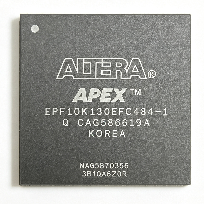
EPF10K130EFC484-1 - FLEX-10KE FPGA 130K Gates 484-BGA | Intel / Altera
The Intel (formerly Altera) EPF10K130EFC484-1 is a FLEX-10KE family Field-Programmable Gate Array (FPGA) delivering 130,000 typical gates and 6,656 logic elements in a 484-ball FineLine BGA (FBGA-484) package, operating at speeds up to 333 MHz with a 2.5 V core supply. The -1 speed grade designates the slowest commercial-grade speed bin in this family, optimized for cost-sensitive designs where moderate performance is acceptable. A FLEX-10KE FPGA is an SRAM-based programmable logic device (PLD) that belongs to the broader category of field-programmable gate arrays (FPGAs) within the programmable logic device (PLD) family hierarchy: FPGA -> programmable logic -> logic IC -> integrated circuit -> semiconductor. The FLEX-10KE series was Altera's first embedded programmable logic family offering System-on-a-Programmable-Chip (SOPC) integration via its embedded array blocks (EABs), which combine lookup-table (LUT) logic with dedicated dual-port RAM, allowing designers to implement memory and logic on a single die. Key features of the EPF10K130EFC484-1 include 832 logic array blocks (LABs), 65,536 bits of embedded memory (64 Kbits), 369 user I/O pins, and built-in support for MultiVolt I/O (3.3 V, 2.5 V, 1.8 V, and 5.0 V tolerant). The device supports in-system programmability (ISP) via the IEEE 1149.1 JTAG interface and IEEE 1532 configuration protocols, allowing field upgrades without removing the part from the board. Architecturally, the FLEX-10KE family uses a continuous routing architecture called the FastTrack Interconnect, which provides predictable timing across all logic and routing paths. The 6,656 logic elements can implement combinational and registered logic, while the embedded array blocks provide 4096-bit RAM blocks for FIFO buffers, register files, and small look-up tables. The FineLine BGA-484 package measures 23 x 23 mm with a 1.0 mm ball pitch, enabling compact high-density designs. Typical applications include industrial control systems, telecommunications line cards, PCI bus interfaces, custom ASIC prototyping, and legacy digital signal processing designs that required moderate logic capacity in the late 1990s and early 2000s. The wide I/O count (369 pins) makes it particularly well suited for parallel bus architectures and high-bandwidth glue logic. When designing with this part, ensure your configuration scheme (PS, PPS, JTAG) matches the board's pull-up topology. The 2.5 V core supply requires separate regulation from the I/O rail; design the decoupling network with 0.1 uF ceramic capacitors as close to each supply pin as possible, plus a 33 uF bulk capacitor near the package. This page synthesizes distributor pricing, SameFrame pin-compatible migration paths, and practical design notes not consolidated in the original manufacturer datasheet.
EPF10K130EFC484-2 - FLEX 10KE 130K Gates FPGA | Altera | 484-FBGA
The Altera (Intel) EPF10K130EFC484-2 is a member of the FLEX 10KE family of Field-Programmable Gate Arrays (FPGAs) offering 130,000 gates and 6,656 logic elements (LEs) in a 484-pin Fine-Pitch Ball Grid Array (FineLine BGA) package. It operates from a 2.5 V core supply and is fabricated on a 0.22 µm CMOS process technology, with a maximum internal clock frequency of 333.33 MHz. The device includes 65,536 bits of embedded memory and provides up to 369 user I/O pins, making it a high-density programmable logic solution for telecom, networking, and embedded computing designs. A Field-Programmable Gate Array (FPGA) is a type of programmable logic device (PLD) that contains an array of configurable logic blocks (CLBs), programmable interconnects, and I/O cells, all of which can be reconfigured by the end user after manufacture. The FLEX 10KE architecture belongs to the broader hierarchy: FPGA -> programmable logic -> digital IC -> semiconductor. FPGAs occupy a unique position between fixed-function ASICs (high NRE, low unit cost at volume) and discrete logic (low cost, fixed function), offering hardware-level parallelism with software-driven design flexibility. Key differentiating features of the EPF10K130EFC484-2 include embedded array blocks (EABs) for on-chip SRAM implementation, multi-volt I/O support for interfacing with 2.5 V and 3.3 V logic, and SameFrame pin migration compatibility across the FLEX 10KE BGA family. The -2 speed grade indicates a balance between performance and power consumption, suitable for cost-sensitive volume production. Typical applications for the EPF10K130EFC484-2 include telecommunications infrastructure (DSLAM, SONET/SDH framer, ATM switches), network routers and switches, glue logic replacement, bus interface bridging (PCI, UTOPIA, POS-PHY), and DSP co-processing. Its embedded memory blocks make it well-suited for packet buffering, lookup tables, and FIFO implementations. When designing with this part, verify PCB footprint compatibility using Altera's SameFrame pin-out guide; ensure 2.5 V core and proper I/O bank voltages; and configure the device via the Altera Quartus/MAX+PLUS II toolchain. Note that the FLEX 10KE family is mature and approaching EOL status—long-term availability should be confirmed before new designs. This page synthesizes distributor pricing, drop-in same-package alternatives within the FLEX 10KE BGA family, and practical design notes not found in a single manufacturer datasheet.
EPF10K130EFC484-2N - 130K-Gate FPGA, 484-BBGA | Altera
Altera EPF10K130EFC484-2N is a 130,000-gate FLEX-10KE field-programmable gate array with 6,656 logic cells, 65,536 bits of embedded memory, and 369 user I/Os. The target operates from a 2.5 V supply spanning 2.375 V to 2.625 V and is housed in a 484-ball fine-pitch BGA package measuring 23 mm by 23 mm. Verified distributor data also lists a commercial operating-temperature range of 0 °C to 70 °C. An FPGA is a field-programmable gate array: a semiconductor device containing programmable logic elements, routing resources, and configurable I/O that engineers can program after manufacturing. FPGAs occupy the programmable-logic tier between fixed-function application-specific integrated circuits and software-controlled processors. They implement digital datapaths, control logic, interfaces, and state machines in configurable hardware, while the FLEX-10KE family combines embedded programmable logic with embedded memory for system-on-a-programmable-chip designs. The defining capability is 130,000 gates supported by 6,656 cells, which gives the device meaningful capacity for multi-interface glue logic and moderate digital systems. Its 65,536 RAM bits support buffers, state storage, lookup tables, and small FIFOs. A 369-I/O budget accommodates many external buses and peripheral interfaces, while 0.22 µm CMOS technology and a listed 333.33 MHz frequency reflect the device family and fabrication generation represented in the verified source data. The architecture is based on logic-array blocks and programmable interconnects rather than fixed execution instructions. Configuration data determines logic functions and signal routing, so changes can be implemented through FPGA design software without replacing the IC. The embedded memory is distributed within this programmable fabric, allowing compact implementations that might otherwise require external memory devices for small storage or queue functions. Typical uses include industrial control and automation, communications-interface bridging, test and measurement equipment, and legacy digital systems requiring a dense programmable BGA device. The 369 available I/Os are especially useful when aggregating parallel buses, memory interfaces, counters, and protocol adapters. The 23 mm by 23 mm FBGA package is intended for space-conscious boards but requires appropriate BGA assembly, inspection, routing, and thermal design capabilities. Designers should verify all configuration, clock, power, signal-integrity, and ball-assignment details against the manufacturer datasheet before release. They should also validate timing at the selected speed grade and supply condition rather than assuming the listed family frequency applies to every implemented circuit. BGA escape routing, contiguous ground references, decoupling placement, and manufacturing-process controls are central to reliable operation. This page consolidates verified distributor specifications, package information, sourcing evidence, application guidance, and drop-in comparison limits. The cross-reference data identifies closely related family and speed-grade candidates, but only candidates with defensible same-package, pin-to-pin evidence are treated as drop-in alternatives.
EPF10K130EFC484-3 - 130K Gates FLEX 10KE FPGA, 484-BGA | Altera
The Intel (formerly Altera) EPF10K130EFC484-3 is a high-density member of the FLEX 10KE embedded programmable logic family, providing approximately 130,000 system gates and 6,656 logic elements (LEs) housed in a 484-pin FineLine Ball-Grid Array (FBGA) package. It offers 369 user I/O pins, 65,536 bits of embedded SRAM, and 832 Logic Array Blocks (LABs) operating on a 3.3 V core supply with multi-voltage I/O support. An FPGA (Field Programmable Gate Array) is a semiconductor integrated circuit whose logic function is defined after manufacturing through configuration memory; FPGAs are widely used as glue logic, prototyping vehicles, and short-to-medium-volume custom compute blocks. The FLEX 10KE family in particular introduced an embedded array block concept that pairs distributed logic with dedicated RAM blocks, enabling System-on-a-Programmable-Chip (SOPC) integration by combining microprocessor cores, custom datapath logic, and on-chip memory in a single device. Key features include 6,656 logic elements, 832 LABs each containing 8 LEs, 65,536 bits of embedded array SRAM organized as 16 EABs (Embedded Array Blocks) of 4,096 bits each, a propagation delay of approximately 0.6 ns per LE, and 369 user I/Os. The device supports in-system programmability via serial or parallel configuration and operates across the commercial 0 C to 70 C temperature range with a -3 speed grade denoting the slowest of three performance bins. The architecture combines a fine-grained logic fabric with course-grained EABs that can implement RAM, ROM, FIFO, or multiplier functions. Multivolt I/O pins support 5.0 V, 3.3 V, and 2.5 V interfaces, allowing direct bridging between legacy TTL/CMOS peripherals and modern low-voltage ASICs without external level shifters. The 484-FBGA package offers high I/O density with a controlled-impedance substrate suitable for high-speed parallel buses and DDR memory interfaces. Typical applications include telecommunications line cards and crosspoint switches, industrial motor-control and machine-vision front ends, ASIC prototyping, military/aerospace signal processing (with the military-grade screening variant), and embedded DSP glue logic between microprocessors and peripherals. The wide I/O count makes the EPF10K130EFC484-3 particularly attractive for parallel bus aggregation in legacy replacement designs. When designing with this part, allocate at least one configuration device (EPC2 or compatible) or a microprocessor-driven configuration scheme, since the FLEX 10KE is SRAM-based and reconfigures on every power-up. Ensure controlled-impedance routing for all clocks and high-speed I/O, and verify that the FBGA land pattern matches your PCB manufacturer's BGA process capability. This page synthesizes distributor pricing snapshots, same-package alternatives, and practical design guidance not assembled in the original FLEX 10KE datasheet, providing a single reference for engineers evaluating end-of-life FLEX 10KE designs against current alternatives.
EPF10K130EFC484-3N - 130K Gates FLEX-10KE FPGA | Intel | 484-BGA
The Intel (Altera) EPF10K130EFC484-3N is a high-density member of the FLEX 10KE family of Field-Programmable Gate Arrays (FPGAs), integrating 6656 logic elements (LEs) and 65536 bits of embedded SRAM in a 484-ball FineLine BGA package with 369 user I/O pins. The "-3N" speed grade denotes a commercial-temperature, faster-than-3 timing bin optimized for higher system clock frequencies in cost-sensitive, non-industrial designs. An FPGA (Field-Programmable Gate Array) is a semiconductor integrated circuit built around an array of configurable logic blocks (CLBs / LEs) interconnected by a programmable routing fabric. Modern FPGAs also embed hard IP such as block RAM, PLLs, and high-speed transceivers. Positioned in the broader programmable logic hierarchy (CPLD -> FPGA -> SoC FPGA), FPGAs deliver the highest logic density and are used when ASIC-like performance is required but design flexibility must be preserved. Key features of the EPF10K130EFC484-3N include 6,656 logic elements, 65,536 bits of embedded SRAM, 72 embedded array blocks (EABs) for memory-intensive functions, and 369 maximum user I/O. The device is built on a 0.22 µm CMOS process and operates from a 2.5 V core supply with multi-voltage I/O support. The 484-ball FineLine BGA (23 × 23 mm, 1.0 mm pitch) provides ample signal breakout for high-pin-count designs while remaining compatible with conventional PCB assembly. Architecturally, the FLEX 10KE family combines Look-Up Table (LUT)-based logic elements with Embedded Array Blocks (EABs) that can implement RAM, ROM, or multiplier functions, giving designers a balanced mix of distributed and block memory. The 2.5 V core with hot-socketing-capable I/O simplifies multi-voltage interfacing, and the in-system programmability via SRAM configuration cells allows rapid design iteration without rework. Typical applications include telecom line-card glue logic, industrial control and instrumentation, prototype ASIC verification, and high-density data-path implementation such as image processing and protocol bridging. The combination of 130 K typical gates and 369 user I/O also makes it suitable for legacy designs migrating from older Altera FLEX 8000 devices that need higher I/O and memory bandwidth. When designing with the EPF10K130EFC484-3N, ensure the configuration scheme (PS, PPS, JTAG, or Altera serial) is selected early in the design cycle, since the configuration pins are multiplexed with user I/O and require careful Quartus II fitter planning. The 484-BGA package also demands controlled-impedance PCB layout and thermal vias under the die for reliable operation in space-constrained boards. This page synthesizes distributor pricing, same-family drop-in alternatives, and practical design notes not found in the manufacturer datasheet alone.
EPF10K130EFC672-1X - FLEX 10KE FPGA 130K Gates 672-FBGA | Intel
The Intel (formerly Altera) EPF10K130EFC672-1X is a member of the FLEX 10KE family of SRAM-based Field Programmable Gate Arrays (FPGAs), delivering 130,000 typical gates and 6,656 logic elements (LEs) in a 672-ball FineLine BGA package. Built on a 0.22 µm CMOS process, it operates from a 2.5 V core supply (2.375 V to 2.625 V) and provides 413 user I/Os with multi-volt I/O support, making it suitable for high-density glue logic, bus bridging, and ASIC prototyping in industrial and telecom designs. A Field Programmable Gate Array (FPGA) is a reprogrammable semiconductor device whose logic function is defined by an SRAM configuration bitstream rather than fixed mask interconnect. FPGAs sit at the top of the programmable logic hierarchy (PLD -> CPLD -> FPGA -> SoC FPGA) and integrate programmable logic fabric, dedicated memory blocks, and I/O cells into a single die. Within this taxonomy, the FLEX 10KE family represents the high-density, embedded-memory generation that preceded the Cyclone series, providing distributed Look-Up Table (LUT) logic with embedded array blocks (EABs) usable as RAM, ROM, or FIFO buffers. Key features include 65,536 bits of embedded SRAM, 832 Logic Array Blocks (LABs), support for 333.33 MHz internal operation, JTAG-compliant IEEE Std 1149.1 boundary-scan test, in-system reconfigurability via the passive serial or ByteBlaster interfaces, and a 4.6 ns pin-to-pin logic delay class typical of the family. The -1X speed grade and commercial temperature grade (0 °C to +70 °C) are explicitly marked on the device top-side per the Altera ordering scheme. Architecturally, the EPF10K130E integrates a continuous, fine-grained logic fabric of 4-input LUTs and 8-LAB clusters, interconnected via a multi-level routing network called the FastTrack Interconnect. Each LAB contains ten LEs and local interconnect; embedded array blocks (EABs) provide 2 Kbit blocks of dual-port RAM for FIFOs, ROM, or look-up-table coefficient storage. This combination enabled designers to implement DSP-style datapath functions without external memory. Typical applications include telecommunications line-card glue logic, industrial control backplanes, ASIC prototyping for medium-complexity designs, and legacy PCI/ISA bridge implementations. Designers migrating from FLEX 10K to FLEX 10KE typically retain their original pin-out footprints while gaining faster I/O registers and additional embedded memory. When designing with this device, note that configuration data is volatile - the bitstream must be reloaded at every power-up from a serial PROM, flash, or micro-controller. The 672-FBGA package is a 27 mm × 27 mm body with 1.0 mm ball pitch; PCB land pattern and reflow profile must conform to JEDEC J-STD-020 moisture sensitivity level handling requirements for large BGAs. This page synthesizes distributor pricing, supply-chain alternatives, and practical engineering guidance not assembled in the original Altera datasheet, including verified availability across Rochester Electronics, DigiKey, and Mouser channels as of 2026-09-11.
EPF10K130EFC672-2 - 130K Gates FLEX 10KE FPGA | Altera | 672-BGA
The Altera EPF10K130EFC672-2 is a member of the FLEX 10KE family of Field-Programmable Gate Arrays (FPGAs), delivering approximately 130,000 gates with 6,656 logic elements and 65,536 bits of embedded memory in a 672-pin FineLine BGA package. Built on a 0.22 µm CMOS SRAM process, this device operates from a 2.5 V core supply and provides 413 user I/Os with internal propagation delays on the order of 0.6 ns, enabling high-performance glue-logic, bus-interface, and DSP pre-processing designs. An FPGA (Field-Programmable Gate Array) is a programmable logic device belonging to the broader category of programmable logic devices (PLDs), sitting alongside CPLDs in the integrated-circuit taxonomy: FPGA -> programmable logic -> logic IC -> integrated circuit. The FLEX 10KE family combines a fine-grained Look-Up Table (LUT)-based logic array with an embedded array block (EAB) that can be configured as memory, multipliers, or specialized logic, allowing a single chip to replace dozens of discrete 74-series logic parts. Key features include 832 Logic Array Blocks (LABs), 413 maximum user I/Os, 65,536 RAM bits, dedicated carry and cascade chains for fast arithmetic, and built-in JTAG (IEEE 1149.1) boundary-scan support. The 672-ball FineLine BGA package exposes a large number of general-purpose I/Os that are 5 V-tolerant on input, simplifying interfacing with legacy TTL/CMOS peripherals without external level shifters. Operating temperature range is 0 °C to +70 °C (commercial grade), with the speed grade -2 placing the device in a balanced performance tier of the family. Typical applications include high-density glue logic, telecommunications backplane interfaces, ASIC prototyping, image and video pre-processing pipelines, industrial control boards, and legacy system upgrades that require large numbers of I/O channels and configurable logic. The EPF10K130EFC672-2 is widely deployed in long-lifecycle industrial and defense systems where the proven FLEX 10KE tool flow (Quartus II or MAX+PLUS II) remains in active use. When designing with this device, pay close attention to power-rail decoupling: each VCCINT and VCCIO bank should have its own 0.1 µF and 10 µF ceramic capacitor pair placed within 5 mm of the BGA balls. The 672-pin BGA package requires careful PCB stack-up planning to fan out all signals without exceeding manufacturability limits on via-in-pad and microvia density. This page synthesizes distributor stock data, drop-in alternatives, and practical design notes that go beyond the manufacturer datasheet to support engineers maintaining FLEX 10KE designs.
EPF10K130EFC672-2X - FLEX 10KE FPGA, 6656 LEs, 672-BGA | Intel
The Intel (formerly Altera) EPF10K130EFC672-2X is a high-density FLEX 10KE family Field-Programmable Gate Array (FPGA) with 6656 logic elements (LEs), 65536 embedded RAM bits, and 413 user I/Os, housed in a 672-ball FineLine BGA package (672-FBGA, 27x27 mm). The -2X speed grade designation indicates an industrial-grade operating temperature range with the second-tier speed performance offered by the FLEX 10KE series. The device is built on a 0.22 μm CMOS SRAM process and operates from a 2.5 V core supply with 3.3 V I/O tolerance. A Field-Programmable Gate Array (FPGA) is a type of programmable logic device that combines an array of configurable logic blocks (CLBs), programmable interconnect, and configurable I/Os on a single die. Within the broader semiconductor taxonomy, an FPGA sits below custom ASICs in NRE cost and above fixed-function CPLDs in logic capacity. The FLEX 10KE family introduced the industry's first embedded programmable logic device (PLD) family, providing System-on-a-Programmable-Chip (SOPC) integration with an embedded array block (EAB) usable as on-chip RAM, ROM, or product-term logic. Key features of the EPF10K130EFC672-2X include 832 Logic Array Blocks (LABs) each containing 8 LEs for a total of 6656 LEs, four Delay-Locked Loops (DLLs) for clock skew management, MultiVolt I/O support for interfacing to 5.0 V, 3.3 V, and 2.5 V logic families, and JTAG-compliant IEEE 1149.1 boundary-scan test capability. The 65536-bit embedded array block (EAB) can be configured as RAM, ROM, or FIFO without consuming logic resources. The 672-FBGA FineLine BGA package provides a 27x27 mm footprint with 1.0 mm ball pitch and a 1.27 mm ball spacing, enabling high-density board routing. The device supports in-system configuration via the serial configuration device interface, allowing field upgrades without removing the board from its system. The FLEX 10KE architecture is widely documented in legacy Altera reference designs and is supported by the legacy MAX+PLUS II and Quartus II design tools. Typical applications for the EPF10K130EFC672-2X include telecommunications glue logic, industrial control and instrumentation, legacy PCI/ISA bus interface bridges, prototyping and emulation platforms, and replacement of multiple discrete logic devices in legacy telecom and test equipment. The 65536-bit embedded RAM and 413 user I/Os make the part well suited for system-level integration in mid-to-late-1990s and early-2000s equipment designs. When designing with this device, engineers should note that the FLEX 10KE series is a mature product line. The Intel/Altera Quartus II toolchain (version 13.1 and earlier) and MAX+PLUS II legacy toolchain provide full synthesis and place-and-route support. New designs targeting modern high-speed SERDES, DSP blocks, or transceivers should consider the Cyclone or Arria device families instead. This page synthesizes distributor pricing, drop-in alternatives, and practical design notes not found on the manufacturer product page or in the standard datasheet cover page.
EPF10K130EFI484-2 - 130K Gates FLEX 10KE FPGA | Intel | BGA-484
The Intel (formerly Altera) EPF10K130EFI484-2 is a 130,000-gate FLEX 10KE family Field Programmable Gate Array (FPGA) with 6,656 logic cells and 274 user I/Os, housed in a 484-ball FineLine BGA package. The part is built on a 0.22 µm CMOS process, supports a 2.5 V core supply, operates from 0 °C to 70 °C, and is rated for a 333.33 MHz internal clock with a 0.6 ns propagation delay at the I/O register. A Field Programmable Gate Array (FPGA) is a type of integrated circuit that can be reconfigured by the designer after manufacturing to implement arbitrary digital logic. FPGAs occupy a place in the broader semiconductor hierarchy between ASICs (Application-Specific Integrated Circuits, which are fixed at fabrication) and general-purpose processors (which execute software sequentially). The FLEX 10KE family was Altera's first embedded programmable logic family to combine a logic array block (LAB) fabric with an embedded array block (EAB) for on-chip RAM/ROM, providing System-on-a-Programmable-Chip (SOPC) integration. Key features of the EPF10K130EFI484-2 include the FLEX 10KE embedded array architecture, 65,536 bits of distributed memory (via EAB), 3.3 V PCI-compliant I/O, JTAG-compliant boundary-scan (IEEE 1149.1) support, and built-in SameFrame pin migration that lets the designer move between 10K, 10KE, 10KA, and 10K130E family devices without board rework when using the FineLine BGA footprint. Typical applications include high-volume telecommunications line cards, glue logic and bus bridging for embedded CPU boards, industrial control and factory automation backplanes, and legacy replacement designs where the long-life FLEX 10KE supply chain and SameFrame migration tool flow reduce board respin risk. Designers using Quartus II or MAX+PLUS II can target this device directly. When designing with this device, treat the 484-ball FineLine BGA as a non-trivial BGA layout: keep all power and ground balls decoupled with 0.1 µF and 10 µF capacitors placed as close to the package as the breakout allows, and verify SameFrame pin-out migration in the Quartus pin planner before committing to a layout because some I/O banks differ between FLEX 10KE and 10KA devices.