Memory ICs
Subcategories
Products (476)
AS4C256M16D3L-12BCN - 4Gbit DDR3L SDRAM 800MHz | Alliance Memory
The AS4C256M16D3L-12BCN is a 4Gbit DDR3L SDRAM organized as 256M x 16, operating at 1.35V with a maximum clock frequency of 800MHz (data rate 1600Mbps). It is housed in a 96-ball FBGA package (9x13mm) and is RoHS compliant and halogen-free. This memory IC is designed for high-performance computing, networking, and industrial applications requiring low power consumption and high bandwidth. DDR3L (Double Data Rate 3 Low Voltage) is a type of synchronous dynamic random-access memory (SDRAM) that operates at a reduced supply voltage of 1.35V, compared to standard DDR3's 1.5V. This lower voltage reduces power consumption by up to 20% while maintaining similar performance, making it ideal for power-sensitive applications such as laptops, embedded systems, and networking equipment. DDR3L is part of the DDR SDRAM family, which includes DDR, DDR2, DDR3, and DDR4, each offering increased speed and lower power. Key features include a parallel interface with a 16-bit data bus, 800MHz clock speed, and a CAS latency of 20ns. The device supports JEDEC clock jitter specifications, ensuring reliable operation in high-speed systems. The 96-ball FBGA package provides excellent thermal and electrical performance, with a compact footprint suitable for space-constrained designs. The AS4C256M16D3L-12BCN utilizes advanced CMOS technology to achieve high density and low power consumption. It supports various burst lengths and programmable CAS latency, allowing flexibility in system design. The device also includes on-die termination (ODT) and dynamic ODT for improved signal integrity, reducing the need for external termination resistors. Typical applications include networking equipment (routers, switches), industrial automation, embedded computing, and consumer electronics such as set-top boxes and smart TVs. Its low voltage and high bandwidth make it suitable for DDR3L-based systems requiring 4Gbit density. When designing with this memory, ensure proper decoupling capacitors near the power pins and follow the layout guidelines in the datasheet to minimize signal integrity issues. The device requires a 1.35V supply and a separate VDDQ, which should be regulated accurately.
AS4C256M16D3L-12BCNTR - 4Gbit DDR3L SDRAM 96-FBGA | Alliance Memory
The AS4C256M16D3L-12BCNTR is a 4Gbit DDR3L SDRAM organized as 256M x 16, operating at 1.35V with a maximum clock frequency of 800 MHz (data rate 1600 Mbps/pin). It is housed in a 96-ball FBGA package (9x13mm) and is designed for commercial temperature range (0°C to +95°C). This memory IC is a drop-in replacement for standard DDR3L components, offering high-speed double-data-rate transfer for applications requiring large, low-power memory. DDR3L (Double Data Rate 3 Low Voltage) SDRAM is a type of synchronous dynamic random-access memory that operates at a reduced supply voltage of 1.35V, compared to standard DDR3's 1.5V, reducing power consumption by up to 20% while maintaining similar performance. It is part of the DDR3 memory family, which uses double-data-rate signaling to transfer data on both edges of the clock, achieving high bandwidth. DDR3L is widely used in mobile devices, embedded systems, and networking equipment where power efficiency is critical. Key features include a parallel interface with 16-bit data bus, 800 MHz clock speed, 20 ns access time, and support for 1.283V to 1.45V supply voltage. The device is RoHS compliant and lead-free, meeting environmental standards. The 96-FBGA package with 9x13mm dimensions provides a compact footprint suitable for space-constrained PCB designs. Technically, the AS4C256M16D3L-12BCNTR utilizes advanced DRAM process technology to achieve high density and low power. It supports burst lengths of 8 and 4, on-die termination (ODT), and programmable CAS latency. The device includes auto-refresh and self-refresh modes for power saving. The 1.35V operation reduces I/O power, making it ideal for battery-powered applications. Typical applications include servers, workstations, networking equipment, and embedded systems requiring high-capacity, low-power memory. The 4Gbit density and 16-bit organization make it suitable for memory expansion in industrial PCs, routers, and test equipment. When designing with this component, ensure proper decoupling capacitors near the power pins and follow the layout guidelines in the datasheet to minimize signal integrity issues. The device requires a stable 1.35V supply and reference voltage (VREF) for reliable operation.
AS4C256M16D3LC-12BIN - 4Gb DDR3L SDRAM 96-FBGA | Alliance Memory
The AS4C256M16D3LC-12BIN is a 4Gb DDR3L SDRAM organized as 256M x 16 bits, operating at 1.35V with a data rate of 800 MHz (DDR3L-1600). It comes in a 96-ball FBGA package (7.5x13.5mm) and is designed for industrial temperature range (-40°C to +95°C). This memory IC is a drop-in replacement for standard DDR3L modules, offering high-speed data transfer and low power consumption. DDR3L SDRAM is a type of dynamic random-access memory that operates at a lower voltage (1.35V) compared to standard DDR3 (1.5V), reducing power consumption by about 20% while maintaining similar performance. It is part of the DDR3 family, which uses double data rate architecture to transfer data on both edges of the clock, achieving high bandwidth. DDR3L is commonly used in embedded systems, networking equipment, and industrial applications where power efficiency and reliability are critical. Key features include an 8-bank architecture, programmable CAS latency, burst lengths of 8 and 4, on-die termination (ODT), and a 20ns row cycle time. The device supports auto-refresh and self-refresh modes, and includes a temperature sensor for thermal management. The 96-ball FBGA package provides a compact footprint suitable for space-constrained designs. Technically, the AS4C256M16D3LC-12BIN uses a high-speed CMOS process and features a 16-bit data bus, achieving data rates up to 1600 Mbps per pin. It operates from a single 1.35V supply, with an I/O voltage of 1.35V, and is compatible with JEDEC DDR3L standards. The device includes programmable read and write latencies, and supports DLL (Delay-Locked Loop) for precise timing. Typical applications include embedded computing, industrial PCs, networking routers, and automotive infotainment systems. Its low voltage and industrial temperature range make it ideal for harsh environments. The device is also suitable for high-reliability systems requiring long-term availability. When designing with this memory, ensure proper decoupling capacitors near the power pins and follow the layout guidelines in the datasheet to minimize signal integrity issues. The device requires a stable 1.35V supply and careful termination of the data and address lines.
AS4C256M8D3LB-12BIN - 2Gbit DDR3L SDRAM 78-FBGA | Alliance Memory
The AS4C256M8D3LB-12BIN is a 2Gbit DDR3L SDRAM organized as 256M x 8 bits, operating at a clock frequency of 800 MHz (DDR3L-1600) with a CAS latency of 11 and a tRCD/tRP of 13.75 ns. It is housed in a 78-ball FBGA package (8x10.5 mm) and operates from a 1.35V supply, with a voltage range of 1.283V to 1.45V. This device is designed for low-power applications, offering a significant reduction in power consumption compared to standard DDR3. DDR3L (Double Data Rate 3 Low Voltage) is a type of synchronous dynamic random-access memory (SDRAM) that operates at a lower voltage (1.35V) than standard DDR3 (1.5V), reducing power consumption by up to 20% while maintaining similar performance. It is part of the memory hierarchy in computing systems, serving as the main system memory in laptops, embedded systems, and networking equipment. DDR3L is backward compatible with DDR3 slots in many cases, making it a popular choice for upgrades and new designs. Key features include a parallel interface with a data rate of 1600 MT/s, a burst length of 8, and on-die termination (ODT) for improved signal integrity. The device supports auto-refresh and self-refresh modes, with a typical refresh period of 7.8 us at 85°C. It also features programmable CAS latency, additive latency, and write latency, allowing flexibility in system timing. The 78-FBGA package is optimized for space-constrained designs, with a compact footprint of 8x10.5 mm. Technically, the AS4C256M8D3LB-12BIN uses a 2Gbit DRAM cell array with a 8n-prefetch architecture, enabling high-speed data transfer. The device includes a DLL (Delay-Locked Loop) for precise clock alignment and supports dynamic ODT for improved signal quality. It is fabricated using a advanced CMOS process, ensuring low leakage and high reliability. The operating temperature range is 0°C to +95°C (case temperature), making it suitable for commercial and industrial applications. Typical applications include embedded systems, networking equipment (routers, switches), industrial computing, and consumer electronics such as set-top boxes and smart TVs. Its low voltage and high density make it ideal for battery-powered devices and energy-efficient designs. The device is also used in automotive infotainment systems where reliability and temperature range are critical. When designing with this memory, ensure proper decoupling capacitors are placed near the VDD and VDDQ pins to minimize noise. The VREFCA and VREFDQ pins should be bypassed with 0.1uF capacitors. Also, follow the JEDEC DDR3L layout guidelines for signal integrity, especially for high-speed signals. The device supports a 1.35V supply, so ensure the power supply is stable and within the specified range.
AS4C512M16D4-75BIN - 8Gbit DDR4 SDRAM 512Mx16 | Alliance Memory
The AS4C512M16D4-75BIN is an 8Gbit DDR4 SDRAM organized as 512M x 16, operating at a clock frequency of 1.333 GHz (DDR4-2666) with an access time of 18 ns and a write cycle time of 15 ns. It is supplied in a 96-ball FBGA package (7.5x13 mm) and operates from a 1.2V power supply, making it suitable for high-bandwidth memory applications in industrial temperature ranges (-40°C to +95°C). DDR4 SDRAM (Double Data Rate 4 Synchronous Dynamic Random-Access Memory) is a type of volatile memory that transfers data on both edges of the clock signal, doubling the data rate compared to single-data-rate SDRAM. It is the fourth generation of DDR memory, offering higher speed and lower power consumption than its predecessors. DDR4 operates at 1.2V, reducing power by 20% compared to DDR3L, and supports higher densities, making it ideal for servers, networking, and embedded systems. Key features include auto self-refresh, auto precharge, asynchronous reset, output enable, CRC (Cyclic Redundancy Check) function, data mask, write leveling, dynamic on-chip termination (ODT), and ZQ calibration. These features enhance signal integrity and reliability in high-speed systems. The device supports industrial temperature range, ensuring operation in harsh environments. The AS4C512M16D4-75BIN uses a 20nm-class process technology, enabling high density with low power. It features a pseudo-open-drain (POD) interface, which is standard for DDR4, and supports burst lengths of 8 and 4 with burst chop. The memory is organized in 16 banks (4 bank groups), providing high concurrency and reduced latency. Typical applications include networking equipment (routers, switches), industrial computing, embedded systems, and high-performance computing. Its high density and speed make it suitable for buffering and data-intensive tasks. The industrial temperature rating allows use in outdoor and automotive (non-AEC) environments. When designing with this device, ensure proper decoupling with 0.1uF and 1uF capacitors near the power pins, and follow the layout guidelines for DDR4 routing to maintain signal integrity. The ZQ pin requires a 240-ohm resistor to ground for calibration.
AS4C512M16D4A-62BCN - 8Gb DDR4 SDRAM 512Mx16 | Alliance Memory
The AS4C512M16D4A-62BCN is an 8Gb DDR4 SDRAM organized as 512M x 16 bits, operating at 1.2V with a data rate of 1600MHz (3200Mbps). It is housed in a 96-ball FBGA package (7.5x13mm) and is JEDEC standard compliant. This memory IC is designed for high-performance computing, networking, and industrial applications requiring high density and fast data transfer. DDR4 SDRAM (Double Data Rate 4 Synchronous Dynamic Random-Access Memory) is a type of volatile memory that transfers data on both edges of the clock, doubling the data rate compared to DDR3. It operates at lower voltages (1.2V) for improved power efficiency and features higher density and faster speeds. DDR4 is a key component in modern computing systems, servers, and embedded devices, providing the main memory for processors and other digital systems. Key features include a fast clock rate of 1600MHz, 18ns CAS latency, and a 96-ball FBGA package with a 7.5x13mm footprint. The device supports commercial temperature range (0°C to 95°C) and is available in tray packaging. It is fully JEDEC compliant, ensuring compatibility with standard DDR4 memory controllers. Technically, the AS4C512M16D4A-62BCN uses a 16n prefetch architecture, enabling high-speed data transfer. It includes on-die termination (ODT) and programmable read/write latencies for signal integrity. The device also supports auto-refresh and self-refresh modes for power saving. The 1.2V supply reduces power consumption by 20% compared to DDR3L, making it suitable for power-sensitive applications. Typical applications include servers, networking equipment, industrial PCs, and high-end embedded systems. Its high density and speed make it ideal for data-intensive tasks such as real-time analytics, network processing, and industrial automation. The 512M x 16 organization is particularly suited for systems requiring wide data buses. When designing with this component, ensure proper decoupling capacitors near the power pins and follow the layout guidelines in the datasheet to maintain signal integrity at 1600MHz. The device requires a 1.2V supply and a separate VPP voltage of 2.5V for wordline boost.
AS4C512M16D4A-62BCNTR - 8Gb DDR4 SDRAM 512Mx16 | Alliance Memory
The AS4C512M16D4A-62BCNTR is an 8Gb DDR4 SDRAM organized as 512M x 16 bits, operating at 1.2V with a fast clock rate of 1600MHz (DDR4-3200). It is housed in a 96-ball FBGA package (7.5x13mm) and is JEDEC standard compliant, ensuring compatibility with standard DDR4 memory controllers. This device is designed for high-bandwidth, low-power applications, making it ideal for networking, computing, and industrial systems. DDR4 SDRAM (Double Data Rate 4 Synchronous Dynamic Random-Access Memory) is a type of volatile memory that transfers data on both edges of the clock signal, doubling the data rate compared to DDR3. It operates at a lower voltage (1.2V) than DDR3 (1.5V), reducing power consumption. DDR4 is the industry standard for modern computing, offering higher density and speed while maintaining backward compatibility with JEDEC standards. Key features include a 1.2V power supply, 1600MHz clock rate (PC4-3200), 18ns CAS latency, and a 96-ball FBGA package. The device supports on-die termination (ODT), programmable read/write latencies, and auto-refresh and self-refresh modes. It is available in commercial temperature range (0°C to +95°C) and is RoHS compliant. The AS4C512M16D4A-62BCNTR uses a 20nm-class process technology, offering high density and low power. It features a 16n prefetch architecture, which improves bandwidth efficiency. The device includes a temperature sensor for thermal management and supports DLL (Delay-Locked Loop) for precise timing. Typical applications include servers, networking equipment, industrial PCs, and embedded systems requiring high-capacity, high-speed memory. Its 512M x 16 organization is ideal for systems with a 16-bit data bus, such as high-end routers and switches. When designing with this device, ensure proper decoupling capacitors near the power pins and follow the layout guidelines in the datasheet to minimize signal integrity issues. The device requires a 1.2V supply and a separate VPP (2.5V) for wordline boost, which must be generated correctly.
AS4C512M16D4A-62BIN - 8Gb DDR4 SDRAM 512Mx16 | Alliance Memory
The AS4C512M16D4A-62BIN is an 8Gb DDR4 SDRAM organized as 512M x 16 bits, operating at a clock rate of 1600MHz (DDR4-3200) with a data rate of 3.2Gbps per pin. It is housed in a 96-ball FBGA package (7.5x13mm) and operates from a 1.2V supply, compliant with JEDEC standards. This industrial temperature grade device supports a temperature range of -40°C to +95°C, making it suitable for demanding environments. DDR4 SDRAM is a type of synchronous dynamic random-access memory that achieves higher speed and lower power consumption than previous generations. It uses a double data rate interface, transferring data on both edges of the clock, and operates at a lower voltage (1.2V) compared to DDR3 (1.5V). DDR4 is the standard memory technology for modern computing systems, servers, and embedded applications, offering improved bandwidth and efficiency. Key features include a fast clock rate of 1600MHz, burst lengths of 8 and 4 (with burst chop), programmable CAS latency, and on-die termination (ODT) for signal integrity. The device supports auto-refresh and self-refresh modes, and includes a temperature sensor for thermal management. The 96-ball FBGA package provides a compact footprint with excellent thermal and electrical performance. The AS4C512M16D4A-62BIN utilizes advanced DRAM process technology, achieving high density with low power consumption. It features a pseudo-open-drain (POD) interface, which reduces I/O power and improves signal integrity. The device includes a mode register for configuration, and supports various test modes for system validation. Typical applications include networking equipment, industrial computing, automotive infotainment, and embedded systems requiring high-density, high-bandwidth memory. Its industrial temperature range and reliability make it ideal for harsh environments. When designing with this device, ensure proper decoupling and signal integrity practices, including controlled impedance traces and termination. The device requires a stable 1.2V supply and a separate VPP supply of 2.5V for wordline boost.
AS4C512M16D4B-62BCNTR - 8Gb DDR4 SDRAM 512Mx16 | Alliance Memory
The AS4C512M16D4B-62BCNTR is a high-performance 8Gb DDR4 SDRAM organized as 512M x 16 bits, manufactured by Alliance Memory, Inc. It operates at a clock speed of 1600 MHz (DDR4-3200) with a data rate of 3200 MT/s, and is housed in a 96-ball FBGA package (7.5x13 mm). The device uses a 1.2V power supply, with a voltage range of 1.14V to 1.26V, and supports commercial temperature range from 0°C to 95°C. This memory IC is designed for high-bandwidth applications requiring fast data transfer and low power consumption. DDR4 SDRAM (Double Data Rate 4 Synchronous Dynamic Random-Access Memory) is a type of volatile memory that transfers data on both rising and falling edges of the clock signal, effectively doubling the data rate. It is the fourth generation of DDR memory, succeeding DDR3, and offers higher speed, lower voltage, and increased density. DDR4 is a key component in modern computing systems, including servers, desktops, laptops, and embedded systems, where it serves as the main system memory or as a buffer for high-speed data processing. Key features of the AS4C512M16D4B-62BCNTR include a fast clock rate of 1600 MHz, a CAS latency of 19 ns, and a parallel interface. It is JEDEC standard compliant, ensuring compatibility with industry-standard DDR4 memory controllers. The device supports on-die termination (ODT) and posted CAS, which improve signal integrity and reduce bus turnaround time. The 96-ball FBGA package provides a compact footprint suitable for space-constrained designs. The architecture of the AS4C512M16D4B-62BCNTR utilizes an 8n prefetch design, which allows the internal DRAM core to operate at a lower frequency while the I/O interface transfers data at high speed. This architecture reduces power consumption and improves thermal performance. The device also includes auto-refresh and self-refresh modes to maintain data integrity with minimal power draw. Typical applications for this DDR4 SDRAM include servers, networking equipment, industrial computing, and high-performance embedded systems. Its high density and speed make it ideal for applications requiring large memory capacity and fast data throughput, such as data centers, cloud computing, and advanced driver-assistance systems (ADAS). When designing with this component, ensure proper decoupling capacitors are placed near the power pins to minimize noise. The device requires a stable 1.2V supply and careful PCB layout to maintain signal integrity at high speeds. Refer to the datasheet for detailed timing and layout guidelines.
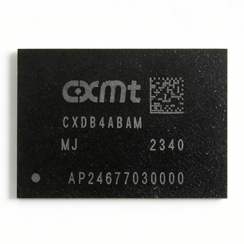
CXDB4ABAM - 2GB LPDDR4X SDRAM 3733Mbps | CXMT
The CXDB4ABAM is a 2GB LPDDR4X SDRAM memory chip manufactured by ChangXin Memory Technologies (CXMT). It operates at a data rate of 3733 Mbps and is housed in a 200-ball FBGA package (15x10x0.8mm). This low-power double data rate memory is designed for mobile, embedded, and consumer applications requiring high bandwidth and low power consumption. LPDDR4X is a type of synchronous dynamic random-access memory (SDRAM) that is part of the LPDDR (Low Power Double Data Rate) family, which is optimized for battery-powered devices. It is a successor to LPDDR4 and offers reduced I/O voltage (0.6V) compared to LPDDR4 (1.1V), resulting in lower power consumption while maintaining similar performance. LPDDR4X is widely used in smartphones, tablets, ultra-thin laptops, and embedded systems where power efficiency is critical. Key features of the CXDB4ABAM include a 2GB density, 3733 Mbps data rate, and support for dual-channel operation. The device uses a 200-ball FBGA package with a 0.8mm ball pitch, enabling compact PCB designs. It is RoHS compliant and supports industrial temperature ranges, making it suitable for a variety of applications. The CXDB4ABAM utilizes advanced DRAM process technology to achieve high speed and low power. It supports various power-saving modes, including idle, self-refresh, and deep power-down, which are essential for extending battery life in portable devices. The memory interface is compatible with standard LPDDR4X controllers, simplifying integration into SoC designs. Typical applications include smartphones, tablets, embedded computing, AI edge devices, and automotive infotainment systems. The high bandwidth and low power make it ideal for applications requiring fast data processing and long battery life. When designing with the CXDB4ABAM, ensure proper decoupling and signal integrity practices are followed. The 0.6V I/O voltage requires careful PCB layout to minimize noise and maintain signal integrity at high data rates.
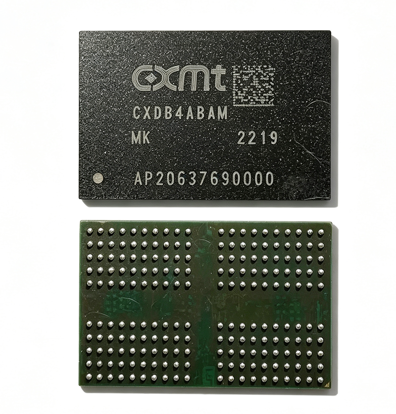
CXDB4ABAM-MK - 8Gb LPDDR4X SDRAM 3733MHz | CXMT
The CXDB4ABAM-MK is a high-performance LPDDR4X SDRAM memory chip manufactured by ChangXin Memory Technologies (CXMT). It operates at a data rate of 3733 MHz, delivering high-speed data transfer for mobile and computing applications. The device is housed in a 200-ball FBGA package (BGA-200, 15x10x0.8 mm), which supports high-density PCB designs with efficient thermal performance. As an LPDDR4X device, it offers low power consumption, making it ideal for battery-powered devices. LPDDR4X (Low Power Double Data Rate 4X) is a type of synchronous dynamic random-access memory (SDRAM) designed for mobile and embedded systems. It is an evolution of LPDDR4, offering higher data rates and lower power consumption through reduced I/O voltage (0.6V). LPDDR4X is part of the broader DRAM memory hierarchy, which includes DDR4, DDR5, and LPDDR5, and is specifically optimized for power-sensitive applications such as smartphones, tablets, and IoT devices. Key features of the CXDB4ABAM-MK include a 3733 MHz data rate, 8Gb density, and support for dual-channel operation. The device operates from a 1.8V VDD1 and 1.1V VDD2 power supply, with a VDDQ of 0.6V for the I/O, reducing power consumption by up to 20% compared to LPDDR4. It supports various operating modes including active, standby, and deep power-down, enabling efficient power management. The package is RoHS compliant, meeting environmental standards. The CXDB4ABAM-MK utilizes advanced process technology to achieve high speed and low power. It features on-die termination (ODT) for improved signal integrity and supports a 16n prefetch architecture, which enhances data throughput. The device includes a temperature-compensated self-refresh (TCSR) mechanism to maintain data integrity across a wide temperature range. The 200-ball FBGA package provides excellent thermal dissipation and is suitable for space-constrained designs. Typical applications include smartphones, tablets, set-top boxes, and IoT devices. In smartphones, the high data rate enables smooth multitasking and immersive VR experiences. In set-top boxes, it supports high-definition video streaming and fast app loading. The low power consumption extends battery life in portable devices. When designing with this device, ensure proper decoupling capacitors are placed near the power pins to minimize noise. The device requires a stable power supply and careful PCB layout to maintain signal integrity at 3733 MHz. Refer to the datasheet for detailed layout guidelines.
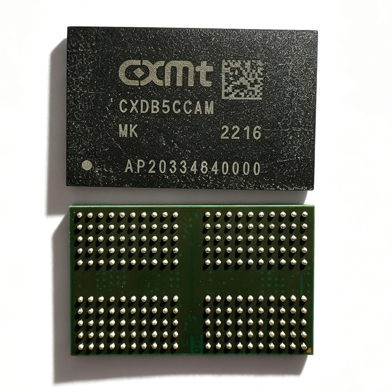
CXDB5CCAM-MK - LPDDR4X SDRAM 8Gb | CXMT | Mobile & AI
The CXDB5CCAM-MK is a high-performance LPDDR4X SDRAM manufactured by ChangXin Memory Technologies (CXMT), designed for mobile, embedded, and AI applications requiring high bandwidth and low power consumption. It features a 200-ball BGA package (BGA200) and operates over a temperature range of -25°C to +85°C, making it suitable for a wide variety of consumer and industrial devices. LPDDR4X (Low Power Double Data Rate 4X) is a type of synchronous dynamic random-access memory (SDRAM) optimized for low power consumption and high data rates, commonly used in smartphones, tablets, and embedded systems. It is part of the LPDDR memory family, which evolved from DDR to provide reduced voltage and power for mobile applications. LPDDR4X operates at a lower I/O voltage (0.6V) compared to LPDDR4 (1.1V), enabling significant power savings while maintaining high bandwidth. Key features of the CXDB5CCAM-MK include support for asynchronous reset, data mask function, and ZQ calibration, which are essential for reliable memory operation. The device is RoHS compliant, ensuring environmental safety. The BGA200 package offers a compact footprint suitable for space-constrained designs, and the -25°C to +85°C operating temperature range supports both commercial and industrial applications. Technically, the CXDB5CCAM-MK is a 8Gb (gigabit) LPDDR4X device, organized as 512M x 16, providing a 16-bit data bus. It supports data rates up to 4266 Mbps, delivering high bandwidth for demanding applications. The memory uses a 1.1V core voltage and 0.6V I/O voltage, reducing power consumption by up to 40% compared to LPDDR4. The device includes on-die ECC and supports deep power-down mode for extended battery life. Typical applications include smartphones, tablets, AI edge devices, and automotive infotainment systems. The CXDB5CCAM-MK is also used in Rockchip RK3588S-based systems, where it provides the necessary memory bandwidth for high-resolution displays and AI processing. Its low power consumption makes it ideal for battery-powered devices. When designing with this memory, ensure proper PCB layout for high-speed signals, including impedance matching and minimal trace lengths. Use the ZQ calibration feature to optimize signal integrity. The device supports a wide range of operating conditions, but careful attention to power supply decoupling is recommended to maintain stable operation.
E3AD8G16A4-HR - 8Gb DDR4 SDRAM 512Mx16 | ELIXIR/NANYA
The E3AD8G16A4-HR is a high-performance DDR4 SDRAM device from ELIXIR/NANYA, organized as 512M x 16 bits, providing 8 Gigabits of memory density. It operates from a 1.2V power supply and is housed in a 96-ball TFBGA package, making it suitable for space-constrained applications requiring high bandwidth and low power consumption. DDR4 SDRAM (Double Data Rate 4 Synchronous Dynamic Random-Access Memory) is a type of volatile memory that transfers data on both edges of the clock signal, effectively doubling the data rate compared to DDR3. It is the industry standard for main memory in servers, desktops, laptops, and embedded systems, offering higher speed, lower voltage, and improved reliability over previous generations. DDR4 modules are essential for applications demanding high memory bandwidth, such as artificial intelligence, big data analytics, and high-performance computing. Key features of the E3AD8G16A4-HR include a data rate of 3200 MT/s (megatransfers per second), a CAS latency of 22, and support for on-die ECC (Error Correction Code) to enhance data integrity. The device also features a programmable read/write preamble, a 10-bit data bus inversion, and a 16n prefetch architecture, which contribute to its high-speed operation and signal integrity. The 1.2V supply voltage reduces power consumption by approximately 20% compared to DDR3L, making it ideal for power-sensitive designs. Technically, the E3AD8G16A4-HR utilizes a 16n prefetch architecture with a 4-bank group design, enabling efficient data access and improved bandwidth utilization. It supports a burst length of 8 and a burst chop of 4, allowing flexible data transfer modes. The device includes a temperature-compensated self-refresh (TCSR) feature that adjusts refresh rates based on operating temperature, optimizing power consumption and reliability. The TFBGA-96 package offers excellent thermal performance and a compact footprint, facilitating high-density PCB layouts. Typical applications for the E3AD8G16A4-HR include high-performance computing systems, networking equipment, industrial automation, and automotive infotainment systems. Its high density and speed make it suitable for use in servers, data centers, and advanced driver-assistance systems (ADAS) where rapid data processing is critical. When designing with this device, ensure proper signal integrity by maintaining controlled impedance traces and minimizing crosstalk. The 1.2V supply should be well-regulated and decoupled with high-frequency capacitors near the power pins. Additionally, follow the JEDEC DDR4 layout guidelines to achieve optimal performance and reliability.
EDB2432B4MA-1DAUT-F-R - 2Gbit LPDDR2 DRAM 533MHz | Micron
The Micron EDB2432B4MA-1DAUT-F-R is an automotive-grade 2Gbit LPDDR2 SDRAM memory IC organized as 64M x 32, operating at 533 MHz and housed in a 134-ball VFBGA package measuring 10 x 11.5 mm. Supply voltage spans 1.14 V to 1.3 V, and the operating temperature range is -40C to +125C, qualifying the device for automotive and harsh-environment electronics. LPDDR2 (Low Power Double Data Rate 2) is a type of synchronous DRAM optimized for mobile and embedded systems. As a member of the broader DDR SDRAM family and power-management-aware memory hierarchy, LPDDR2 reduces core voltage compared with DDR3 and integrates the memory controller interface functions that simplify designs in battery-powered and thermally constrained platforms such as telematics control units, infotainment processors, and ADAS domains. Key features of this device include a parallel interface, double-die package (DDP) architecture that packs two dies in a single 134-VFBGA footprint to achieve 2 Gbit density, a 32-bit data bus width, and the -1D speed grade supporting a 533 MHz clock rate. The automotive temperature rating (indicated by AUT in the ordering code) and lead-free F-thermally enhanced ball assignment make it suitable for under-dash and near-engine electronic modules. Architecturally, the DDP configuration presents a unified 64M x 32 organization across two stacked dies, with chip-select-based die selection handled by the LPDDR2 host controller. Micron fabricates the part on a low-voltage process that keeps I/O and core rails within the JEDEC LPDDR2 1.2 V class, minimizing power dissipation in standby and self-refresh states. Typical applications include automotive infotainment head units, instrument clusters, telematics gateways, ADAS sensor-fusion processors, and rugged industrial embedded boards where a 2 Gbit LPDDR2 with wide temperature tolerance is required alongside application processors such as those from NXP, Renesas, or TI. When designing with this memory, verify that your host controller supports the DDP chip-select mapping and confirm power-rail sequencing for VDD1/VDD2 per the manufacturer datasheet. This page synthesizes distributor pricing, drop-in alternatives within the EDB2432B4 family, and practical design guidance not consolidated in the manufacturer datasheet. Prices are as of 2026-09-03.
EDB4432BBBJ-1DAUT-F-D - 4Gbit LPDDR2 SDRAM 533MHz | Micron
The Micron Technology EDB4432BBBJ-1DAUT-F-D is a 4 Gbit Mobile LPDDR2 SDRAM memory IC with a parallel interface, a 533 MHz clock frequency, and a 128M x 32 memory organization, housed in a 134-ball Fine-Pitch Ball Grid Array (134-FBGA, 10 x 11.5 mm) package for surface-mount applications. LPDDR2 (Low Power Double Data Rate 2) is a JEDEC-defined SDRAM family optimized for battery-powered and thermally constrained systems. Compared to standard DDR SDRAM, LPDDR2 reduces core voltage and adds low-power states such as deep power-down and self-refresh, making it a key building block in the mobile power-management hierarchy alongside application processors, PMICs, and NOR/NAND flash. Key features of this device include 4 Gbit density in a single x32组织 die, a 533 MHz data-rate class supporting high-bandwidth streaming, an extended operating temperature range of -40C to +125C for industrial and automotive-adjacent environments, and the FBGA package that minimizes parasitic inductance for signal integrity at high data rates. The marking code for this device is D9XCB, and the -D suffix designates the industrial temperature variant. Architecturally, the memory uses a banked DRAM core with LPDDR2 CA (command/address) multiplexed signaling, which reduces pin count and simplifies PCB routing versus conventional DDR interfaces. The 1.2V-class core supply of LPDDR2 lowers dynamic power substantially compared to 1.5V DDR3-class solutions, which directly extends battery life in portable designs. Typical applications include embedded industrial computing, networking equipment buffering, automotive infotainment and telematics memory, and portable medical or test instruments where an application processor requires 4 Gbit of high-bandwidth working memory over an LPDDR2 interface. A key design consideration is LPDDR2 fly-by-free point-to-point routing: keep trace-length matching tight between the CA bus and clock, and follow the memory controller vendor's guidelines for on-die-termination settings and ZQ calibration to guarantee eye margins at 533 MHz. This page synthesizes distributor pricing context, drop-in family alternatives, and practical design notes not consolidated in the manufacturer datasheet.
EP1M350B780C5 - Altera Mercury PLD FPGA Configuration Device
The Altera (now Intel) EP1M350B780C5 is an enhanced configuration device belonging to the Altera Mercury PLD family, designed as a single-device, high-speed configuration solution for very-high-density FPGAs. The 780-pin BGA package supports high-density configuration storage, and the part is offered in commercial grade operating conditions with a peak reflow rating of 220 °C. The Mercury configuration device family targets dense Stratix and Cyclone-series FPGA configuration bitstreams, enabling fast parallel configuration of large devices. A configuration device is a non-volatile memory IC specifically architected to store and stream FPGA configuration bitstreams at power-up. Unlike generic flash memory, enhanced configuration devices integrate a dedicated configuration controller block alongside the flash array, which handles the FPGA configuration protocol, error detection, and clock generation. This dedicated hardware offloads the host processor and enables faster, more reliable FPGA boot than serial flash + microcontroller schemes. Configuration devices sit in the broader hierarchy: non-volatile memory -> flash memory -> configuration memory -> FPGA boot companion IC. Key features of the EP1M350B780C5 include a 780-ball BGA package suitable for high-pin-count board layouts, industrial-temperature-grade variants, and compatibility with the Altera enhanced configuration protocol. The device typically pairs with high-density Altera FPGAs (Mercury, Stratix, Cyclone families) where configuration bitstreams exceed the capacity of smaller EPCS or EPCQ devices. It supports multi-device configuration chains and offers programmable configuration modes. The architecture combines a flash memory core with a configuration controller state machine. At power-up the controller reads the stored bitstream and drives it onto the FPGA's configuration data, DCLK, nCONFIG, and nSTATUS pins according to the Altera enhanced configuration specification. This eliminates the need for an external microcontroller and reduces bill-of-material cost in production systems. Typical applications include boot configuration for Altera Stratix-series FPGAs in telecom line cards, Cyclone-series FPGAs in industrial control boards, and any design requiring reliable single-chip FPGA configuration. The 780 BGA package also enables high-speed parallel configuration of the largest Stratix devices in networking and signal-processing systems. When designing with this part, ensure the FPGA's configuration mode pins select the enhanced configuration scheme, and verify that the device's density matches the FPGA's bitstream size. Verify peak reflow compatibility (220 °C) with the board's assembly profile. This page synthesizes distributor pricing, drop-in alternatives, and practical design notes not found on a single manufacturer datasheet, providing context for sourcing and lifecycle decisions.
EP2A25F724 - Altera APEX II Enhanced Configuration Device | FPGA
The Altera (now Intel) EP2A25F724 is an enhanced configuration device (EPC) designed for high-density SRAM-based FPGAs in the Altera APEX II family, including the EP2A25 and other EP2A-series devices. The EP2A25F724 integrates a configuration controller and flash memory in a single package, providing a single-device, high-speed, advanced configuration solution for very high-density FPGAs and eliminating the need for external boot PROMs. An enhanced configuration device (EPC) is a non-volatile memory IC specialized for storing FPGA configuration bitstreams and presenting them to the target FPGA at power-up via a vendor-specific configuration interface (typically FLEX/APEX passive serial or passive parallel). EPCs sit at the bottom of the boot-memory hierarchy (EPC -> configuration memory -> non-volatile memory -> semiconductor memory) and translate JTAG/serial commands into configuration cycles. By combining flash and controller logic in one die, the EP2A25F724 reduces BOM count, board area, and configuration time relative to discrete flash plus CPLD solutions. Key features of the EP2A25F724 include support for multi-device configuration chains, built-in JTAG support, in-system programmability (ISP) through the IEEE Std. 1149.1 boundary-scan interface, and on-chip oscillator and control logic. The device supports Altera's passive serial, passive parallel asynchronous, and passive parallel synchronous configuration modes, making it compatible with both APEX II and legacy FLEX devices. It is offered in a 724-pin FineLine BGA package suitable for high-density production designs. Architecturally, the EP2A25F724 separates the flash array into configuration controller blocks and user-accessible flash regions, allowing engineers to store configuration data and user code in the same physical device. The configuration controller handles bitstream compression, decompression, and error detection during FPGA load, while the flash array retains data across power cycles without a backup battery. Typical applications include APEX II FPGA boot memory, multi-FPGA configuration in telecom and networking line cards, industrial vision and signal processing platforms, and military/aerospace systems requiring field-upgradable firmware. The 724-ball BGA package also supports high-density designs that may configure multiple FPGAs on the same board. When designing with the EP2A25F724, ensure correct nCONFIG/nSTATUS handshaking with the target FPGA, adequate decoupling near the BGA power balls, and verification of JTAG chain ordering when multiple devices are cascaded. Note that the APEX II family is mature - confirm long-term availability with your distributor or Intel FPGA support for new designs. This page synthesizes verified distributor pricing, package details, and a curated set of pin-compatible Altera EPC drop-in alternatives not found in the manufacturer datasheet alone.
EPC1064LC20 - 65kb OTP Config PROM 20-PLCC | Intel
The Intel EPC1064LC20 is a 65-kilobit one-time-programmable (OTP) configuration memory device designed for serial configuration of SRAM-based Altera/Intel FPGAs, packaged in a 20-pin J-lead PLCC (LC20) case and rated for commercial 0 C to 70 C operation. It stores up to 65,536 bits of configuration bitstream and uses a 5 V single supply with 4.5 V to 5.5 V operating range, delivering configuration data to the target FPGA over a serial interface at access times around 90 ns (~10 MHz). The EPC1064LC20 targets legacy Altera device families including ACEX 1K, APEX 20K, APEX II, FLEX 10K, FLEX 6000, Mercury, Stratix, Stratix GX, Stratix II and Stratix II GX, and is also a usable configuration source for many Cyclone and Cyclone II boards designed around the EPC1/EPC2 daisy-chain protocol. A configuration PROM (also called a configuration device) is a non-volatile memory that holds the FPGA bitstream and reloads it at every power-up, reset, or reconfiguration event because SRAM-based LUT devices are volatile and lose their logic configuration when power is removed. Within the broader component hierarchy, configuration PROMs sit under Memory ICs > non-volatile memory > PROM, and are used in the boot path of every SRAM-based FPGA. The EPC1064LC20 occupies the OTP sub-category, trading re-programmability for low unit cost and a compact 20-PLCC footprint. Key features of the EPC1064LC20 include 65,536 bits of storage (8,192 bytes), a serial data interface that streams configuration bits to the host FPGA on power-up, 5 V single-supply operation with 4.5 V to 5.5 V tolerance, and commercial-grade 0 C to 70 C temperature range. The 20-pin PLCC (LC) package provides a through-hole-compatible J-lead footprint that is widely supported on legacy development boards and easy to socket for factory programming or field replacement. The EPC1064LC20 uses a simple internal state machine that streams configuration data out of an internal OTP array when the host FPGA asserts nSTATUS and drives DCLK, then tri-states after the DONE pin is released. Because the configuration clock is generated by the FPGA in passive-serial mode, no external oscillator is needed; the PROM simply shifts bits in lock-step with DCLK. The interface is intentionally minimal so the device can replace battery-backed configuration modules at a fraction of the BOM cost in low-to-mid density FPGA designs. Typical applications for the EPC1064LC20 include boot memory for ACEX 1K and FLEX 10K designs, configuration storage for industrial controllers built around Stratix and APEX 20K, prototyping platforms using Mercury or APEX II FPGAs, and cost-sensitive legacy retrofits where the original EPC1064 has gone obsolete. Designers also use it as a single-chip boot source for multi-device FPGAs that accept passive serial configuration. When designing with the EPC1064LC20, confirm that the host FPGA's configuration mode pins are strapped for passive-serial (PS) mode and that DCLK frequency stays within the PROM's ~10 MHz access budget. For new designs, prefer an EPCQ or EPCQ-L device in 16-pin SOIC for higher density and faster configuration; the EPC1064LC20 is best reserved for legacy PCB revs and exact-form-factor retrofits. This page synthesizes distributor pricing, same-family OTP variants, and PCB-retrofit design notes for engineers maintaining or replicating EPC1064LC20-based systems.

EPC1064PC8 - 65kb OTP Config PROM for FPGAs, PDIP-8 | Intel/Altera
The Intel (formerly Altera) EPC1064PC8 is an OTP (One-Time Programmable) configuration memory device sized 65 kb (65,536 bits) and packaged in an 8-pin PDIP (PC8) through-hole package, designed to store the configuration bitstream for Altera FPGA families such as the FLEX, MAX 9000, and Classic EPLD series. It is supplied from a 5 V VCC rail, supports serial data output to the target FPGA's DATA/DCLK configuration pins, and is specified over the commercial 0C to +70C operating range. The PC8 suffix denotes the plastic DIP-8 (0.300 inch, 0.1 inch lead pitch) package option, while the underlying silicon is identical to the EPC1064 family members sold in PLCC and SOIC packages. A Configuration PROM is a non-volatile memory (NVM) device that holds the FPGA configuration bitstream and serially shifts it into the FPGA during power-up, allowing the FPGA to be re-configured at every power cycle without an external parallel boot ROM. Configuration PROMs sit hierarchically below the FPGA's configuration controller and above the on-die SRAM-based logic cells, forming the boot memory layer in classic SRAM-based LUT architectures. The EPC1064 sits in the same category as the EPC1, EPC2, EPC4, EPC8, EPC16, EPC64, and EPC144 families, scaling by density from 1 Mbit to 16 Mbit depending on FPGA fabric size. Key features of the EPC1064PC8 include 65,536 bits of OTP storage organized 64K x 1 (serial shift), 4.75 V to 5.25 V single-supply operation, dedicated nCONFIG/nSTATUS/CE handshake pins for FPGA handshaking, a maximum DCLK toggle rate of approximately 8 MHz in fast-mode, and a serial configuration time under 100 ms for typical bitstreams. Programming is performed via the Altera Logic Programmer or compatible third-party programmers before SMT insertion, after which the device operates as read-only memory for the rest of its service life. Typical applications include legacy Altera FPGA configuration storage (FLEX 10K, FLEX 8000, MAX 9000), industrial control boards with soldered-down FPGA logic, CPLD prototyping carriers, and educational FPGA development boards that need a permanent boot image. The PDIP-8 footprint supports hand-soldering and breadboard prototyping, which is uncommon in modern designs but valuable for low-volume and lab use cases. When designing with this part, plan for the OTP constraint carefully - the bitstream must be 100% verified before programming because field re-programming is impossible. Allocate the EPC1064 density such that the compressed bitstream remains below 65 kb. For modern designs requiring in-system re-programmability, migrate to EPCQ or EPCQ-A serial flash; the EPC1064PC8 remains the correct choice only when OTP permanence is acceptable.
EPC1064PI8 - 64Kb OTP FPGA Config PROM 8-PDIP | Altera
The Altera EPC1064PI8 is an OTP (One-Time Programmable) configuration memory device for FPGAs, providing 64 Kb (65,536 bits) of non-volatile storage in an 8-pin PDIP through-hole package. It is part of Altera's enhanced configuration device family and operates from a single 5V supply, delivering configuration data to Altera FPGAs at clock rates up to 6 MHz. What is a configuration PROM? A configuration PROM (Programmable Read-Only Memory) is a non-volatile memory device specifically designed to store FPGA bitstream data. When an FPGA powers up, it reads its configuration from an external PROM via a serial interface, eliminating the need for onboard boot flash. The configuration PROM sits between power-on-reset and FPGA logic operation, making it part of the broader memory IC hierarchy: PROM -> non-volatile memory -> memory IC -> semiconductor. Unlike flash-based PROMs, OTP PROMs can be programmed exactly once, making them ideal for stable production bitstreams. Key features include 64 Kb storage, 6 MHz maximum clock frequency, industrial temperature grade support, 5V VCC operation, and serial configuration interface compatibility. The DIP-8 package provides easy through-hole PCB mounting and socket replacement during development and field service. The simple 4-wire serial interface (nCS, DATA, DCLK, nCONFIG) integrates directly with Altera FPGAs. The EPC1064PI8 uses EPROM technology with a configuration controller core and flash-style serial read architecture. Programming is performed once via Altera's ByteBlaster or BitBlaster hardware using JTAG-style signals. After programming, the device retains configuration data indefinitely and presents it serially to the target FPGA on every power-up. Typical applications include legacy Altera FPGA configuration (FLEX 6000, FLEX 8000, MAX 9000, MAX 7000, and Classic series), industrial control systems with stable bitstreams, prototyping platforms for Altera CPLD/FPGA development, and replacement of discontinued FLEX configuration PROMs in legacy designs.
EPC1064TC32 - 65kb OTP Config PROM for FPGAs | Altera | 32-TQFP
The Altera EPC1064TC32 is an OTP (One-Time Programmable) configuration memory device designed to store FPGA configuration bitstreams for Altera's classic MAX 9000 and FLEX family FPGAs, organized as 64K x 1 bit serial memory in a 32-pin TQFP (7x7 mm) package. It supports a single 5V supply (4.75V to 5.25V), operates from 0C to +70C commercial temperature, and provides non-volatile serial configuration storage of 65,536 bits (8,192 bytes). What is a configuration PROM? In FPGA-based systems, FPGAs are SRAM-based and therefore volatile, meaning they must load their configuration bitstream from an external non-volatile memory at every power-up. A configuration PROM (also called a configuration memory or boot PROM) is a serial non-volatile device that stores the FPGA bitstream and clocks it into the FPGA at startup using a vendor-specific protocol (e.g., Altera's FLEX configuration scheme). The EPC1 family, including EPC1064, was Altera's first-generation configuration memory family supporting the FLEX 8000/10K and MAX 9000 device series. Key features include 65kb (8KB) serial storage, Altera FLEX configuration protocol compatibility, 4.75V to 5.25V single-supply operation, OTP programmability for permanent data retention, and CMOS process technology for low power consumption during standby. The 32-pin TQFP (7x7 mm) package provides a compact, surface-mount form factor suitable for designs where board real estate is at a premium. Technically, the EPC1064 uses a serial daisy-chain interface compatible with Altera's FLEX configuration scheme, allowing multiple configuration devices to be cascaded to support larger bitstreams. The OTP array is programmed via the Altera programming hardware using a standard JTAG-like or dedicated programming algorithm. Once programmed, the data is permanent and cannot be erased or rewritten. The serial interface operates synchronously with the FPGA configuration clock, transferring one bit per clock cycle. Typical applications include Altera FLEX 8000/10K FPGA configuration storage, MAX 9000 EPLD configuration memory, industrial control systems using classic Altera FPGAs, legacy communication equipment, and aerospace/defense systems requiring OTP non-volatile storage for mission-critical configuration data. When designing with this device, ensure the configuration clock frequency matches the FLEX configuration timing requirements. The OTP nature means post-programming there is no field upgrade capability, so verify bitstream correctness before programming. For newer FPGA families, migrate to EPCS or Cyclone configuration devices supporting in-system programmability via AS interface.
EPC1064VLC20 - 64Kb OTP FPGA Config PROM | Altera | 20-PLCC
The Altera EPC1064VLC20 is a 65,536-bit (212,942 x 1 organization, per legacy datasheet framing as a 64 Kb one-time-programmable serial configuration memory) OTP configuration PROM designed to load bitstream data into SRAM-based Altera/Intel FPGA and CPLD devices at system power-up. Housed in a 20-pin PLCC (J-lead, 9 x 9 mm body), the part operates from a single 5.0 V supply and exposes a serial daisy-chain interface that allows multiple EPC devices to be cascaded for designs that exceed a single PROM's density. The die is one-time programmable, so once a bitstream is fused it cannot be rewritten in-circuit; this is the classic trade-off of the EPC family versus the later EPCS/EPCQ erasable serial flash parts. A configuration PROM is a non-volatile serial memory that holds the FPGA's configuration bitstream and streams it to the FPGA over a small handful of dedicated pins (nCONFIG, nSTATUS, CONF_DONE, DCLK, DATA) at power-up. In the broader component taxonomy, the EPC1064 sits under: configuration memory -> serial PROM -> non-volatile memory -> memory IC -> integrated circuit. It is a child of the EPC1 / EPC1064 family and a predecessor of the EPC1441, EPC2, EPC4, EPC8 and EPC16 successors that scaled density upward (EPC2 introduced 5 V in-system programmability to address the OTP limitation). Key features include 64 Kbit storage organized as 64K x 1, a 5.0 V single-supply requirement, a serial daisy-chain output for cascading, and compatibility with essentially every legacy Altera SRAM-based LUT device family: ACEX 1K, APEX 20K, APEX II, Arria GX, Cyclone, Cyclone II, FLEX 10K, FLEX 6000, Mercury, Stratix, Stratix GX, Stratix II, and Stratix II GX. Operating temperature range is 0C to 70C (commercial grade). Architecturally the device uses an internal oscillator to clock data out of the one-time-programmable memory array; no external configuration clock source is required from the system. The daisy-chain protocol allows up to eight EPC1064 devices to be cascaded to support bitstreams up to roughly 512 Kbits without external steering logic. Programming is performed in a separate Altera programming unit before the part is soldered onto the board - the EPC1064 is not in-system programmable. Typical applications include legacy Altera FPGA boot configuration on industrial controllers, telecom line cards using FLEX 10K or ACEX 1K, military/aerospace retrofits where original EPC1064-bitstreams are still in production, and replacement builds for EOL designs that must remain bit-identical. The 20-PLCC package is socket-friendly, simplifying field replacement in legacy systems. When designing with this part, verify your target FPGA's configuration interface voltage (the EPC1064's 5 V VCC must match the FPGA's VCCIO for the configuration bank; older 5 V-tolerant FPGAs pair natively, while 3.3 V-only devices like Cyclone II require level shifting). Also confirm the cascaded PROM count does not exceed the FPGA's supported configuration clock frequency at startup. The OTP nature means any bitstream change requires a physical PROM swap - budget for that in field-service documentation. This page consolidates distributor pricing as of 2026-09-10, drop-in compatible alternatives in the same 20-PLCC footprint, and practical design notes for integrating the EPC1064VLC20 into legacy Altera FPGA designs not found on a single manufacturer or distributor page.
EPC1064VPC8 - 65kb OTP Config PROM for FPGAs | Altera DIP-8
The Altera EPC1064VPC8 is a one-time-programmable (OTP) configuration PROM designed to store bitstream data for Altera SRAM-based FPGAs, with 65 kb of memory organized as 64K x 1, supplied in an 8-pin PDIP package. It is a member of Altera's EPC1-series configuration memory family and is designed to load configuration data into target FPGAs via a dedicated serial configuration interface at power-up, system initialization, or whenever new configuration data is required. Background Knowledge: An FPGA configuration PROM is a non-volatile memory device that holds the bitstream (logic configuration) for a SRAM-based FPGA. Because SRAM cells lose their contents when power is removed, every power-on cycle must reload the configuration bitstream. A configuration PROM is therefore paired with the target FPGA and acts as the boot source, residing in the FPGA's configuration chain. Hypernym hierarchy: configuration PROM -> non-volatile memory -> memory IC -> integrated circuit -> semiconductor. Synonyms: config PROM, configuration memory, bitstream PROM, FPGA boot PROM. Key features include a 64K x 1 serial organization, OTP (one-time-programmable) anti-fuse programming technology, a 3.0 V to 3.6 V single supply, a serial daisy-chain interface compatible with Altera FPGAs, and 8-pin PDIP through-hole packaging for breadboard-friendly prototyping and legacy designs. The device supports target devices including ACEX 1K, APEX 20K, APEX II, Arria GX, Cyclone, Cyclone II, FLEX 10K, FLEX 6000, Mercury, Stratix, Stratix GX, Stratix II, and Stratix II GX. The EPC1064VPC8 uses Altera's anti-fuse programming cell technology, where each memory bit is a one-time-fusable link that permanently writes a logic '1' or '0' during programming. Anti-fuse cells provide non-volatility without a battery, high security (the bit pattern cannot be read out by simple microprobe), and high radiation tolerance. Programming is performed once via the Altera programming hardware, after which the bitstream is fixed for the life of the device. Typical applications include FPGA boot memory for industrial control boards, legacy Altera development kits, and any design using ACEX 1K, APEX 20K, FLEX 10K, or first-generation Cyclone / Stratix families. Designers use the EPC1064VPC8 when an 8-pin PDIP through-hole footprint is required for easy rework or socketed programming. When designing with this part, ensure the target FPGA's configuration controller supports EPC1-series PROMs and verify the bitstream size does not exceed 65 kb. Because the package is OTP through-hole PDIP, the part is best suited for prototype and low-volume production rather than high-density SMT assemblies.
EPC1064VTC32 - 64Kb OTP Configuration PROM | Altera | 32-TQFP
The Altera EPC1064VTC32 is a 64-kilobit one-time-programmable (OTP) configuration PROM designed to store and load FPGA configuration bitstreams for high-density Altera FPGAs. Housed in a 32-pin Thin Quad Flat Pack (TQFP-32, 7x7 mm) package, it operates from a single 3.0V to 3.6V supply and serves as a single-device, high-speed configuration solution that replaces multiple EPROM/PLD configuration chains in legacy designs. An FPGA configuration PROM is a non-volatile memory device that holds the FPGA's bitstream and serially delivers it at power-up through the FPGA's configuration interface (typically the Altera passive serial, passive parallel, or JTAG scheme). The EPC1064 belongs to Altera's enhanced configuration device family, which integrates a configuration controller and a flash/OTP memory array on one die to simplify board layout and shorten FPGA in-system programming time. Key features include 65,536 bits of OTP storage (organized as one configuration bitstream), an industry-standard 4-pin JTAG (IEEE 1149.1) boundary-scan interface for in-system programming, dedicated FPGA control signals (nSTATUS, CONF_DONE, nCONFIG, DCLK), and a cascading interface that allows multiple EPC devices to be daisy-chained for FPGAs requiring larger bitstreams than 64 Kb. The device is supplied in a surface-mount 32-TQFP package rated for the standard 0C to +70C commercial operating range. Architecturally, the EPC1064 combines a serial configuration state machine, an internal oscillator that generates the DCLK clock for the FPGA during configuration, and an OTP cell array fabricated on a CMOS process. Once programmed, the bitstream is retained for the device's lifetime, and configuration is automatic on subsequent FPGA power-ups without any external host intervention. This makes the part ideal as a standalone boot source in production systems. Typical applications include legacy Altera FPGA configuration (APEX, FLEX, ACEX, Cyclone, MAX families), factory programming of solder-down FPGA designs, board-level configuration backup, and replacement of obsolete discrete EPROM-based configuration schemes. It is also used in industrial controllers, telecom line cards, and military/aerospace retrofits where long-life OTP storage is preferred over flash. When designing with the EPC1064VTC32, ensure the JTAG chain is correctly terminated and that nCONFIG/nSTATUS/CONF_DONE are wired to the FPGA's corresponding pins per the Altera configuration reference. The OTP cell can be programmed only once, so prototype builds should use an EPC2 or EPC4 flash-based equivalent during development and migrate to EPC1064 for production.