RF Transceivers
Products (74)

PN5190B1EV/C121Y - 13.56MHz NFC Frontend IC | NXP Semiconductors
The NXP Semiconductors PN5190B1EV/C121Y is a high-power 13.56 MHz NFC frontend IC (RFID reader/transponder IC) supporting ISO 14443, ISO 15693, ISO 18000-3, ISO 18092, ISO 21481, FeliCa and MIFARE protocols, controlled over SPI from a 2.4 V to 6 V supply, housed in a 64-ball VFBGA package (SOT2062-1, 4.5 mm x 4.5 mm x 0.8 mm). An NFC frontend is a dedicated RF transceiver that generates the 13.56 MHz carrier, modulates and demodulates the contactless air interface, and offloads protocol handling from the host MCU. In the system hierarchy it sits below the application controller and above the antenna matching network, making it the physical layer of an NFC reader, POS terminal or access-control reader. Key features include high RF output power for challenging RF environments, multi-protocol support covering EMVCo-relevant contactless schemes, SPI host interface, and factory initialization with firmware V2.7 supporting encrypted firmware download for secure field updates. NXP states the enhanced feature set simplifies EMVCo 3.0 certification, a major benefit for payment terminal makers. Technically, the PN5190B1 (silicon version B1) requires firmware V2.0 or higher per the datasheet, and the C121Y suffix denotes the firmware/programming variant. The very-thin fine-pitch ball grid array keeps the RF section close to the antenna for superior RF performance in compact reader designs. Typical applications include EMVCo payment terminals, physical access control readers, POS systems, and industrial or handheld NFC devices where difficult RF coupling must be handled reliably. Design consideration: the delivered packaging is 13-inch reel, MSL 3, minimum order quantity 2450 pieces, so plan moisture handling and procurement volume accordingly. This page synthesizes distributor inventory data, the NXP datasheet, and drop-in alternative analysis not found on any single distributor page.

RS9116W-DB00-CC1-B2A - Dual-Band Wi-Fi + BT5 Module | Silicon Labs
The Silicon Labs RS9116W-DB00-CC1-B2A is a dual-band 802.11 a/b/g/n (2.4 GHz and 5 GHz) Wi-Fi plus dual-mode Bluetooth 5 transceiver module in a 155-pin surface-mount LGA package supplied in tray packaging with antenna not included. As a Network Co-Processor (NCP), it offloads the complete wireless, networking, and security stacks from a host MCU, connecting via UART, SPI, or SDIO interfaces. A Wi-Fi module is a self-contained wireless subsystem that integrates the radio transceiver, RF front end, baseband, and protocol stacks on a certified PCB module, sitting within the broader hierarchy of RF transceivers, wireless connectivity ICs, and embedded networking components. Certified modules such as the RS9116W family dramatically shorten regulatory approval cycles because module-level certifications (FCC, IC, ETSI/CE) can be leveraged by the end product. Key features of the RS9116W-DB00-CC1-B2A include dual-band operation covering 2412 MHz to 2484 MHz and 4900 MHz to 5975 MHz, 802.11n high-throughput modes, and Bluetooth 5 dual-mode (BR/EDR and LE) concurrency. The module offers high throughput with power-optimized performance and extended range, making it suitable for battery-sensitive IoT designs. Technically, the RS9116W operates as an NCP: the host MCU sends commands over UART, SPI, or SDIO while the module runs the TCP/IP and security stacks, freeing host flash and RAM. Alternatively, the networking stack can be bypassed for raw-packet operation when the host runs its own stack. Typical applications include industrial gateways, smart meters, connected home hubs, and asset-tracking devices that need robust dual-band Wi-Fi alongside Bluetooth LE provisioning or beaconing. Design consideration: because this variant does not include an antenna, the RF layout requires a well-controlled 50-ohm feed to an external antenna connector or PCB antenna; follow the Silicon Labs reference design for matching network placement. This page synthesizes distributor pricing, drop-in same-family alternatives, and practical design notes not found in the manufacturer datasheet.

RTAX1000SL-CGS624B - 1M-Gate Rad-Tolerant FPGA CCGA-624 | Microchip
The Microchip Technology RTAX1000SL-CGS624B is a radiation-tolerant FPGA delivering 1,000,000 equivalent system gates with 12,096 CLBs and 125,000 ASIC-equivalent gates, housed in a 624-pin ceramic column grid array (CCGA/CGS624) package built on 0.15 um CMOS technology. A radiation-tolerant FPGA is a field-programmable gate array engineered to survive the ionizing radiation environment of space flight, including total ionizing dose (TID) and single-event effects (SEE). Unlike commercial FPGAs, rad-tolerant FPGAs sit at the top of the programmable logic hierarchy (FPGA -> programmable logic IC -> digital IC -> semiconductor) and are qualified for satellite, planetary probe, and launch-vehicle electronics where replacement after deployment is impossible. Key features include the anti-fuse-based RTAX-SL architecture derived from the commercial Axcelerator family, which provides live-at-power-up operation with no configuration device required. The embedded SRAM blocks include built-in FIFO control logic, and the fabric offers segmentable clocks and chip-wide highway routing for large system designs. Speed-grade B devices support system clock rates up to 581 MHz per family datasheets, with a 1.5V core supply. The RTAX-SL fabric integrates embedded SRAM and bus-capable routing in a true single-chip form factor with low power consumption, making it suitable for payloads that must survive launch vibration and multi-year orbital missions. Design migration to RTAX-DSP variants is supported through the same development flow. Typical applications include satellite payload data processing, spacecraft bus control, telemetry and telecommand (TT&C) interfaces, and instrument control in deep-space science missions. A key design consideration: use Microchip Libero SoC with the RTAX-S prototyping methodology (footprint-compatible adaptor board plus EDIF netlist and pinout converter) to validate designs on commercial ProASIC/AX equivalents before committing to flight units. This page synthesizes distributor availability data, same-family drop-in alternatives, and practical radiation-tolerant design notes not consolidated in the manufacturer datasheet.
SAF8444 - 77GHz FMCW Automotive Radar SoC | NXP Semiconductors
The NXP Semiconductors SAF8444 is a 77 GHz automotive FMCW radar system-on-chip (SoC) operating across the 76-81 GHz band, built on 28nm RFCMOS process technology in a compact package for mainstream front and corner radar sensors. An automotive radar SoC is a highly integrated device that combines the RF transceiver front end, radar signal processing, and a microcontroller subsystem on a single die. Within the vehicle sensor hierarchy, it sits at the core of the radar sensor module, upstream of functions such as blind spot detection, automated emergency braking, and L2/L2+ ADAS features, replacing multi-chip discrete radar chains with a single-chip solution. Key features include wideband 76-81 GHz FMCW operation supporting short-, medium-, and long-range sensing, an innovative RF architecture optimized for power efficiency, and advanced interference suppression that improves robustness in dense traffic environments where multiple radar-equipped vehicles operate simultaneously. Technical depth: the SAF8444 is derived from the proven SAF85xx radar platform and fabricated in 28nm RFCMOS. The CMOS-based RF integration simplifies thermal management and reduces system cost compared with SiGe-based radar front ends, and the single-chip integration enables on-sensor L2/L2+ ADAS processing at entry-level vehicle price points. Typical applications include blind spot detection (BSD) corner radar sensors, automated emergency braking (AEB) front radar, and cost-optimized long-range front radar for mainstream and economy EVs, where the power-efficient RFCMOS design reduces cooling requirements in sealed sensor housings. Design consideration: as an automotive-qualified radar SoC, the SAF8444 requires careful antenna-in-package or antenna-on-PCB design and appropriate power sequencing with external flash memory, which is often programmed in-system (as evidenced by dedicated in-system programmers from SMH Technologies). This page synthesizes manufacturer product data, drop-in alternative analysis, and design guidance not found in the manufacturer fact sheet, with pricing references as of 2026-09-14.

ST25R3916B - NFC Initiator with 1.4W Power | STMicroelectronics
The ST25R3916B is a highly integrated NFC initiator and card emulator from STMicroelectronics, designed for high-performance contactless communication. It supports ISO 14443A/B, ISO 15693, and FeliCa protocols, delivering up to 1.4W of output power for extended read range. The device operates from a 2.4V to 5.5V supply and is available in a 32-pin VFQFPN package. An NFC initiator is a device that actively generates an RF field to communicate with passive tags or cards. It is the core component in applications such as point-of-sale terminals, access control readers, and NFC-enabled consumer electronics. The ST25R3916B sits within the NFC reader IC family, which is part of the broader RFID and contactless communication IC category, ultimately falling under wireless communication semiconductors. Key features include a built-in high-efficiency power amplifier that delivers up to 1.4W, dynamic power control for optimal field strength, and advanced anti-collision algorithms for reliable multi-tag reading. The device also integrates a low-power card detection mode, making it suitable for battery-powered applications. Its high sensitivity and noise immunity ensure robust performance in noisy environments. The ST25R3916B employs a sophisticated analog front-end with automatic antenna tuning and calibration, simplifying PCB design and reducing component count. It supports both active and passive load modulation, enabling card emulation and peer-to-peer modes. The device includes a comprehensive set of registers for fine-tuning RF parameters, allowing designers to optimize performance for specific antenna configurations. Typical applications include payment terminals, access control systems, NFC-enabled smart locks, and industrial RFID readers. The high output power extends read range, while the low-power modes preserve battery life in portable devices. The device is also suitable for automotive key fobs and in-vehicle NFC modules. When designing with the ST25R3916B, careful attention must be paid to antenna matching and power supply decoupling. The device requires a clean supply voltage and proper grounding to achieve optimal RF performance. The SPI interface allows easy integration with microcontrollers, and the interrupt output simplifies event-driven firmware design.
ST25R3920B - NFC Reader IC, 13.56MHz, ISO 14443A/B | STMicroelectronics
The ST25R3920B is a high-performance NFC universal reader IC from STMicroelectronics, designed for 13.56 MHz contactless communication. It supports ISO 14443A/B, ISO 15693, and FeliCa protocols, making it a versatile solution for a wide range of NFC applications. The device operates from a 2.4V to 5.5V supply and features an integrated high-power transmitter with programmable output power up to 1.4W, enabling robust communication with passive tags and cards. An NFC reader IC is a specialized radio-frequency integrated circuit that manages the modulation, demodulation, and protocol handling required for near-field communication. It sits at the heart of contactless systems, bridging the digital host interface (typically SPI or I2C) and the analog RF front-end that drives the antenna. In the system hierarchy, the ST25R3920B functions as the physical layer and data-link layer controller, working alongside a host microcontroller (MCU) that runs the application stack. This separation allows designers to implement complex NFC functionality without deep RF expertise. Key features of the ST25R3920B include support for both active and passive peer-to-peer modes, an automatic antenna tuning system, and a low-power field detection mode that enables battery-efficient wake-up. The device also offers a high receiver sensitivity of -70 dBm, ensuring reliable reading of low-signal tags. Its integrated voltage regulator simplifies power supply design, and the SPI interface supports clock speeds up to 10 MHz for fast data transfer. From a technical architecture perspective, the ST25R3920B integrates a highly linear RF front-end with a 13.56 MHz carrier generation circuit, a multi-protocol framing engine, and a flexible FIFO buffer. The device uses a digital demodulator with adaptive filtering to handle various modulation depths and data rates, from 106 kbps to 848 kbps. Its automatic antenna tuning algorithm continuously adjusts the matching network to compensate for environmental detuning, maintaining optimal performance across different antenna designs and operating conditions. Typical applications include point-of-sale terminals, access control systems, NFC-enabled smart locks, and industrial asset tracking. In a POS terminal, the ST25R3920B provides the RF interface for contactless payment cards and mobile wallets, supporting the required EMVCo and NFC Forum compliance. For access control, its low-power field detection allows battery-operated door locks to wake up only when a card is presented, extending battery life. When designing with the ST25R3920B, careful attention must be paid to antenna matching and PCB layout to achieve optimal read range. The device's automatic tuning feature helps, but the antenna coil's inductance and Q-factor must be within the specified range. Additionally, proper decoupling and grounding are essential to minimize noise and ensure stable operation.
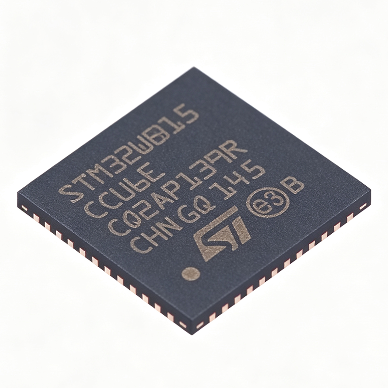
STM32WB15CCU6 - 2.4GHz BLE 5.2 Wireless MCU, 320KB Flash | STMicroelectronics
The STMicroelectronics STM32WB15CCU6 is a dual-core wireless microcontroller integrating a 64 MHz Arm Cortex-M4 application processor and a 32 MHz Arm Cortex-M0+ radio processor, designed for Bluetooth Low Energy 5.2 applications. It features 320 KB of flash memory and 48 KB of SRAM, housed in a 48-pin UFQFPN (UFQFPN-48) package with dimensions of 7x7 mm. The device supports a supply voltage range of 1.71V to 3.6V and operates over a temperature range of -40°C to +105°C, making it suitable for industrial and consumer IoT applications. A wireless microcontroller (MCU) is a system-on-chip that integrates a general-purpose microcontroller core with a radio transceiver, enabling wireless communication protocols such as Bluetooth Low Energy, Zigbee, or proprietary sub-GHz protocols. In the system hierarchy, a wireless MCU sits above a standalone MCU and below a full application processor, providing a balance of processing capability, low power consumption, and wireless connectivity. The STM32WB15CCU6 specifically targets Bluetooth Low Energy 5.2, offering a complete solution for connected devices without requiring an external radio chip. Key features of the STM32WB15CCU6 include a 2.4 GHz radio supporting Bluetooth Low Energy 5.2 with a transmit power of up to +6 dBm and a receiver sensitivity of -96 dBm, ensuring robust wireless links. The dual-core architecture allows the Cortex-M0+ to handle the radio stack independently, freeing the Cortex-M4 for application tasks, which improves real-time performance and reduces power consumption. The device also includes a rich set of peripherals, including multiple UART, SPI, I2C interfaces, a 12-bit ADC, and a random number generator, providing flexibility for various sensor and control applications. From a technical depth perspective, the STM32WB15CCU6 leverages ST's advanced 40nm process technology, enabling low power consumption with multiple low-power modes, including a standby mode with a current consumption of only 1.6 µA. The radio architecture includes a dedicated hardware encryption engine supporting AES-128, AES-256, and other algorithms, ensuring secure wireless communication. The device also features a true random number generator (TRNG) and a unique 96-bit ID, enhancing security for IoT applications. Typical applications include smart home devices such as smart locks, sensors, and lighting controls, as well as healthcare wearables, industrial wireless sensor networks, and asset tracking systems. The STM32WB15CCU6's low power consumption and robust wireless performance make it ideal for battery-powered devices that require long operational lifetimes. When designing with this device, ensure proper antenna matching and PCB layout for the 2.4 GHz radio to achieve optimal range and reliability. The device requires a 32.768 kHz crystal for the low-power RTC and a 32 MHz crystal for the radio, and careful attention to power supply decoupling is essential to minimize noise and ensure stable operation.
STM32WB55RGV6 - Dual-Core BLE 5.3 MCU 1MB Flash | STMicroelectronics
The STMicroelectronics STM32WB55RGV6 is an ultra-low-power multiprotocol wireless microcontroller with a dual-core architecture - an Arm Cortex-M4 with FPU running at 64 MHz for the application and an Arm Cortex-M0+ running at 32 MHz dedicated to the radio stack - with 1 Mbyte of Flash memory, integrated Bluetooth Low Energy 5.3/5.4-compliant and IEEE 802.15.4-2011 radio covering 2.405 GHz to 2.48 GHz, housed in a 68-pin VFQFPN exposed-pad package. A wireless MCU is a microcontroller that integrates both a processing core and a radio transceiver on a single die, sitting at the intersection of the microcontroller and RF transceiver product categories within the broader wireless-connectivity semiconductor hierarchy. By partitioning the real-time radio stack onto the Cortex-M0+ and the user application onto the Cortex-M4, the STM32WB55 family guarantees RF protocol timing independence from application load - a key architectural advantage over single-core BLE MCUs. Key features include 1 MB of Flash and 256 KB of SRAM for application and stack storage, support for Bluetooth 5.3, Thread, and Zigbee protocols on the same silicon, a rich peripheral set (USB 2.0 full-speed device, USART, SPI, I2C, I2S, Quad-SPI, 12-bit ADC, comparators, touch sensing), and ultra-low-power modes with down to a few microamps in Stop 2 with RAM retention. The integrated balun and output power up to +6 dBm (as per family datasheet range) simplify RF front-end design. The dual-core radio architecture offloads BLE/802.15.4 stacks from the application core, so deterministic real-time behavior, security via the Cortex-M0+ trust boundary, and OTA firmware update capability are maintained even under heavy application processing. The 68-pin VFQFPN-EP (7x7 mm class) package provides a good GPIO count for sensor hubs and HMI. Typical applications include smart-home sensors and lighting (Thread/Zigbee), Bluetooth LE beacons and wearables, industrial wireless nodes, and medical monitoring devices. Design consideration: RF layout requires a 50-ohm match to the antenna and solid ground planes on the exposed pad; verify the exact radio output-power and sensitivity figures against the official STM32WB55xx datasheet. This page synthesizes distributor pricing, drop-in alternatives, comparison tables, and design notes not found in the manufacturer datasheet.

STM32WB55VEQ6 - 2.4GHz Dual-Core Wireless MCU | STMicroelectronics
The STMicroelectronics STM32WB55VEQ6 is a dual-core wireless microcontroller that integrates a 64 MHz Arm Cortex-M4 application processor with a 32 MHz Arm Cortex-M0+ dedicated to radio processing, enabling concurrent execution of application code and Bluetooth Low Energy (BLE) 5.0, Zigbee 3.0, and OpenThread stacks. It is housed in a 129-ball UFBGA (VQFN-129) package, offering a compact footprint for space-constrained IoT devices. A wireless microcontroller (MCU) is a system-on-chip that combines a general-purpose processor core with a radio transceiver, allowing embedded systems to communicate wirelessly. The STM32WB55VEQ6 belongs to the STM32WB series, which is part of the broader STM32 family of 32-bit Arm Cortex-M microcontrollers. This hierarchy places it within the categories of wireless MCU -> microcontroller -> embedded processor -> semiconductor, providing a clear taxonomy for engineers selecting components for IoT applications. Key features include 1 Mbyte of flash memory and 256 Kbytes of SRAM, providing ample storage for complex application firmware and protocol stacks. The device supports a wide supply voltage range of 1.71V to 3.6V, making it suitable for battery-powered applications. It also integrates a rich set of analog peripherals, including a 12-bit ADC, operational amplifiers, and comparators, as well as digital interfaces such as SPI, I2C, USART, and USB 2.0 FS. The radio supports BLE 5.0 with a data rate of up to 2 Mbps, Zigbee 3.0, and OpenThread, with a typical sensitivity of -96 dBm for BLE. The dual-core architecture allows the Cortex-M0+ to handle all real-time radio protocol processing, while the Cortex-M4 runs the application code, ensuring deterministic wireless performance without burdening the main processor. The device also features a hardware cryptographic accelerator (AES, RSA, ECC) and a true random number generator (TRNG) for secure communication, which is critical for IoT security. Typical applications include smart home devices (e.g., smart locks, sensors, lighting), industrial wireless sensor networks, healthcare wearables, and asset tracking systems. The low-power modes, including Sleep, Stop, and Standby, with current consumption as low as 1.62 uA in Standby mode, extend battery life in portable applications. When designing with this device, ensure proper antenna matching and RF layout to achieve optimal radio performance. The device requires a 32.768 kHz crystal for the RTC and a 32 MHz crystal for the radio, and careful PCB design is essential to minimize interference between the RF section and digital circuitry.

STM32WBA52CEU6 - Arm Cortex-M33 BLE 5.4 MCU | STMicroelectronics
The STM32WBA52CEU6 is a 32-bit Arm Cortex-M33 microcontroller from STMicroelectronics, featuring a 100 MHz core with TrustZone, DSP instructions, and a floating-point unit (FPU). It integrates a 2.4 GHz radio supporting Bluetooth Low Energy (BLE) 5.4, making it ideal for secure IoT and wireless applications. The device comes in a UFQFPN-48 package (7x7 mm) and operates over a supply voltage range of 1.71V to 3.6V. A microcontroller (MCU) is a compact integrated circuit designed to govern a specific operation in an embedded system. It contains a processor core, memory, and programmable input/output peripherals. The STM32WBA52CEU6 belongs to the STM32WBA series, which is part of the broader STM32 family of 32-bit microcontrollers. This series is optimized for wireless connectivity, combining the Arm Cortex-M33 core with a radio transceiver, enabling secure and low-power communication in IoT devices. Key features include 512 KB of flash memory and 128 KB of SRAM, a rich set of analog and digital peripherals, and advanced security features such as TrustZone, secure boot, and hardware cryptographic accelerators. The BLE 5.4 radio supports long-range, high-throughput, and advertising extensions, with a link budget of up to 105 dB. The device also includes a 12-bit ADC, multiple timers, and communication interfaces like SPI, I2C, USART, and USB. The STM32WBA52CEU6 is built on a low-power process technology, offering multiple low-power modes including Sleep, Stop, and Standby, with typical current consumption as low as 2.2 uA in Standby mode with RTC. The TrustZone technology provides hardware-enforced isolation for secure code execution, making it suitable for applications requiring robust security, such as secure payment, authentication, and firmware protection. Typical applications include smart home devices, industrial sensors, medical wearables, and asset tracking. The integrated BLE radio and security features make it a strong choice for IoT edge nodes that need secure wireless communication. The device supports over-the-air (OTA) firmware updates, enabling remote maintenance and feature updates. When designing with this MCU, ensure proper antenna matching for the BLE radio and follow the layout guidelines in the datasheet to minimize RF interference. The supply voltage should be decoupled with a 100 nF capacitor close to each VDD pin, and the VDDA pin should have a dedicated 1 uF capacitor for analog performance.
STM32WBA55RGV6 - 100MHz Cortex-M33 BLE 5.4 MCU | STMicroelectronics
The STMicroelectronics STM32WBA55RGV6 is a wireless microcontroller (MCU) integrating an Arm Cortex-M33 core running at up to 100 MHz with a 2.4 GHz radio supporting Bluetooth Low Energy (BLE) 5.4, Zigbee, Thread, and proprietary protocols. It is housed in a 28-pin VFQFPN (VG) package with a 4x4 mm footprint, offering a compact solution for connected embedded applications. A wireless MCU is a system-on-chip that combines a general-purpose microcontroller with a radio transceiver, enabling wireless communication in embedded systems. The STM32WBA55RGV6 belongs to the STM32WBA family, which is part of the broader STM32 microcontroller portfolio from STMicroelectronics. This family is designed for low-power, secure, and connected applications, bridging the gap between traditional MCUs and dedicated wireless SoCs. Key features include 512 KB of flash memory and 128 KB of SRAM, providing ample space for application code and data. The device supports a wide supply voltage range of 1.71V to 3.6V, making it suitable for battery-powered designs. It integrates a rich set of peripherals, including multiple UART, SPI, I2C, ADC, timers, and GPIOs, along with advanced security features such as TrustZone, secure boot, and hardware cryptographic accelerators (AES, RSA, ECC). The radio achieves a sensitivity of -96 dBm for BLE, ensuring reliable communication. The STM32WBA55RGV6 is built on a low-power process technology, with multiple low-power modes (Sleep, Stop, Standby) to minimize energy consumption. The Arm Cortex-M33 core with TrustZone provides hardware-enforced isolation for secure applications, while the radio supports concurrent multi-protocol operation, enabling seamless switching between BLE and Zigbee/Thread. This makes it ideal for IoT nodes, smart home devices, and industrial sensors. Typical applications include smart home automation (e.g., smart locks, sensors), wearable health monitors, industrial wireless sensor networks, and asset tracking. The device's low power consumption and robust security features make it well-suited for battery-operated devices that require secure wireless connectivity. When designing with this device, pay attention to antenna matching and RF layout to achieve optimal radio performance. The device requires a 32 MHz crystal for the radio and a 32.768 kHz crystal for low-power timing. Proper decoupling of the supply pins and a clean ground plane are essential for reliable operation.

STM32WBA62CGU6 - BLE 5.4 Multiprotocol MCU 100MHz | ST
The STMicroelectronics STM32WBA62CGU6 is a multiprotocol wireless 32-bit microcontroller with an Arm Cortex-M33 core with TrustZone and FPU running at up to 100 MHz, 2 Mbytes of flash memory and 512 Kbytes of RAM, integrating a 2.4 GHz radio compliant with Bluetooth LE 5.4 and IEEE 802.15.4-2015, housed in a 48-pin UFQFN package with exposed pad. A wireless MCU is a microcontroller that combines a general-purpose processor core with an integrated radio transceiver, allowing a single chip to run both application firmware and a wireless protocol stack. Within the power-management hierarchy, the STM32WBA6 belongs to the STM32 wireless MCU family (STM32WBA series -> STM32 32-bit Arm Cortex MCUs -> microcontrollers -> embedded processors), positioned as the high-end member offering large flash memory for concurrent multi-protocol stacks. Key differentiating features include Bluetooth Low Energy 5.4 and IEEE 802.15.4-2015 radio compliance supporting Zigbee, Thread, and Matter protocols with simultaneous multi-protocol operation, up to 2 Mbytes of flash and 512 Kbytes of RAM for large concurrent stacks, up to 86 GPIOs, and USB high-speed support for advanced connectivity. The device is built on a 40 nm process technology optimized for ultra-low-power operation and is compliant with RED and US security standards. Architecturally, the Cortex-M33 with Arm TrustZone provides hardware-enforced security isolation, essential for Matter certification and secure over-the-air updates. The FPU accelerates signal processing for sensor fusion and audio applications. ST supports development through the STM32CubeWBA firmware package with HAL drivers, BLE, Zigbee, Thread, and Matter middleware. Typical applications include smart-home Matter/Zigbee/Thread hubs, Bluetooth LE sensors and lighting, industrial wireless nodes, and connected building devices where large flash enables dual-image OTA and multi-stack coexistence. Design consideration: multi-protocol concurrent operation increases RAM and flash footprint; budget at least 512 Kbytes RAM headroom and follow the STM32CubeWBA reference designs for RF matching and antenna layout. This page synthesizes distributor inventory data, the manufacturer datasheet and migration application note AN6159, drop-in family alternatives, and practical design guidance not found on any single distributor page.
STM32WBA62PII6 - 100MHz Cortex-M33 BLE MCU | ST | IoT
The STMicroelectronics STM32WBA62PII6 is an ultra-low-power multiprotocol wireless microcontroller built on an Arm Cortex-M33 core with TrustZone and FPU, running at 100 MHz with 2 Mbytes of Flash memory, integrating a Bluetooth Low Energy 5.4 and IEEE 802.15.4 radio in a 121-ball UFBGA package. A wireless MCU (microcontroller unit) combines a general-purpose processor with a 2.4 GHz radio transceiver on a single die. Within the system hierarchy, it sits below full application processors but above simple RF transceivers, since it embeds the CPU, memory, peripherals, and radio needed to run a complete wireless protocol stack such as Bluetooth LE, Zigbee, or Thread natively. Key features include the 100 MHz Cortex-M33 with hardware TrustZone security and floating-point unit, 2 Mbytes of on-chip Flash for stacked protocol applications, and a patented ultra-low-power radio compliant with the Bluetooth SIG Low Energy specification 5.4 and IEEE 802.15.4-2015. Multi-protocol support covers Bluetooth LE, Zigbee, and Thread simultaneously, allowing one hardware design to serve multiple ecosystems. Technically, the STM32WBA6xxx family embeds a radio sub-architecture optimized for concurrent multiprotocol operation with the radio stack firmware executing on the same Cortex-M33 core, reducing BOM cost versus two-chip host-plus-network-processor solutions. TrustZone-based isolation allows secure over-the-air updates and split secure/non-secure application partitions. Typical applications include smart-home Zigbee and Thread devices, Bluetooth LE lighting and sensor nodes, and connected industrial equipment requiring secure 802.15.4 mesh networking. The 121-UFBGA package suits compact, board-constrained designs. For design, plan RF layout carefully around the UFBGA ball field: a continuous ground plane under the antenna feed and 50-ohm controlled impedance matching are essential for radiated compliance. This page synthesizes distributor listings, datasheet facts, family drop-in options, and practical design notes not consolidated in the manufacturer datasheet.

STM32WBA63CIU6 - BLE 6.0 + 802.15.4 Cortex-M33 MCU | ST
The STMicroelectronics STM32WBA63CIU6 is an ultra-low-power multiprotocol wireless microcontroller featuring an Arm Cortex-M33 32-bit core with TrustZone and FPU running at up to 100 MHz, 2 Mbytes of Flash memory, and an integrated 2.4 GHz radio supporting Bluetooth LE 6.0 (v5.4 certified per distributor listings), IEEE 802.15.4-2015, Zigbee, Thread, and Matter, housed in a 48-pin UFQFPN package with exposed pad. A wireless MCU (microcontroller unit) combines a processor core, memory, peripherals, and a radio transceiver on a single die, sitting within the broader hierarchy of 32-bit MCUs -> wireless connectivity MCUs -> system-on-chip (SoC) devices. Multiprotocol wireless MCUs like this one let a single chip and a single PCB design serve multiple connectivity standards, simplifying inventory and certification for smart-building and IoT product lines. Key features include the 100 MHz Cortex-M33 core with TrustZone security isolation and hardware FPU, 2 Mbytes of on-chip Flash for large concurrent protocol stacks and application code, and an ultra-low-power profile engineered for battery-powered devices. The radio subsystem is compliant with Bluetooth LE and IEEE 802.15.4-2015, enabling simultaneous support of Matter-over-Thread and Zigbee ecosystems. Architecturally, the STM32WBA6xxx series is part of ST's STM32WBA family, which pairs the high-efficiency Cortex-M33 pipeline with a dedicated 2.4 GHz radio and security accelerators. TrustZone provides hardware-enforced partitioning between secure and non-secure firmware, which is increasingly required by platform ecosystem certification programs for connected devices. Typical applications include smart-home devices (sensors, actuators, Matter/Thread end nodes), Zigbee lighting and building automation, Bluetooth LE beacons and wearable accessories, and industrial wireless sensor nodes where ultra-low sleep current extends battery life for years. When designing with this device, budget RF layout carefully: the 2.4 GHz radio requires controlled-impedance matching and a solid ground plane on the exposed pad; also verify supply decoupling per the ST datasheet to minimize radio spurs. This page synthesizes distributor pricing, same-family drop-in alternatives, and practical design guidance not found on any single manufacturer or distributor page.
STM32WBA65RIV6 - BLE 5.4 802.15.4 MCU 2MB Flash | ST
The STMicroelectronics STM32WBA65RIV6 is an ultra-low-power multiprotocol wireless microcontroller featuring an Arm Cortex-M33 core with TrustZone and FPU running at 100 MHz, 2 Mbytes of Flash memory, an integrated 2.4 GHz radio compliant with Bluetooth LE 5.4 and IEEE 802.15.4-2015, packaged in a 68-pin VFQFPN with exposed pad. A wireless MCU (microcontroller unit) combines a general-purpose processor, memory, and a radio transceiver on one die, sitting within the hierarchy of embedded processors: MCU -> Arm Cortex-M-based MCU -> wireless SoC -> multiprotocol connectivity IC. Wireless MCUs eliminate the complexity and power cost of a discrete radio-plus-MCU two-chip solution, and the STM32WBA6xxx series is STMicroelectronics' flagship ultra-low-power entry in this class, targeting Bluetooth LE, Zigbee, and Thread mesh networks on a single silicon platform. Key differentiating features include the 100 MHz Cortex-M33 with hardware TrustZone security and FPU, 2 Mbytes of embedded Flash for large application and stack footprints, an ultra-low-power radio supporting Bluetooth SIG Low Energy specification 5.4 and IEEE 802.15.4-2015 (Zigbee and Thread), and independent power domains including a dedicated supply input for the 2.4 GHz radio and an analog independent supply for ADC and comparators. The family offers four packages from 48 to 121 pins, with or without an integrated SMPS option for extended battery life. Architecturally, the device uses ST state-of-the-art patented radio technology with a dedicated 2.4 GHz radio core, allowing concurrent multiprotocol operation and secure over-the-air updates. TrustZone-based isolation partitions secure and non-secure firmware, supporting PSA-aligned security architectures common in smart-home and industrial sensor ecosystems. Typical applications include Zigbee and Thread smart-home devices (sensors, lighting, actuators), Bluetooth LE accessories such as beacons and wearables, and industrial 802.15.4 mesh nodes where ultra-low average current determines battery replacement intervals. Design consideration: plan the RF matching network and power supply partitioning early - the dedicated RADIO supply input and exposed pad require a solid ground pour for RF performance, and the SMPS versus LDO supply variant affects layout and efficiency trade-offs. This page synthesizes distributor pricing, family drop-in variants, comparison data, and practical design notes not found on a single manufacturer datasheet page. Pricing references are as of 2026-09-13.

STM32WL55CCU6 - Dual-core Arm Cortex-M4/M0+ LoRa SoC | STMicroelectronics
The STMicroelectronics STM32WL55CCU6 is a wireless system-on-chip (SoC) that integrates a dual-core Arm Cortex-M4 and Cortex-M0+ processor with a sub-GHz radio supporting LoRa, (G)FSK, (G)MSK, and BPSK modulations. It is housed in a 48-pin UFQFPN package (7x7 mm) and operates over a supply voltage range of 1.8V to 3.6V. The device features 256 KB of flash memory and 64 KB of SRAM, making it suitable for battery-powered IoT applications. A wireless MCU is a microcontroller that integrates a radio transceiver on the same chip, enabling wireless communication without external RF components. The STM32WL55CCU6 belongs to the STM32WL series, which is part of the broader STM32 family of 32-bit microcontrollers. This SoC combines the processing power of an Arm Cortex-M4 core with the energy efficiency of a Cortex-M0+ core, allowing for flexible task partitioning and low-power operation. Key features include a maximum CPU frequency of 48 MHz for both cores, a sub-GHz radio with sensitivity down to -137 dBm (LoRa), and support for LoRaWAN and Sigfox protocols. The device also includes a rich set of peripherals such as 12-bit ADC, DAC, comparators, timers, SPI, I2C, USART, and a random number generator. The integrated radio eliminates the need for an external transceiver, reducing BOM cost and PCB area. The STM32WL55CCU6 is built on ST's low-power process technology, offering multiple low-power modes including Sleep, Stop, and Standby, with current consumption as low as 1.62 uA in Standby mode with RTC. The dual-core architecture allows the Cortex-M0+ to handle radio communication while the Cortex-M4 runs application code, optimizing power and performance. Typical applications include smart agriculture sensors, smart metering, asset tracking, smart city infrastructure, and industrial monitoring. The sub-GHz radio provides long-range communication with low power consumption, making it ideal for battery-operated devices that need to transmit data over kilometers. When designing with this device, ensure proper antenna matching and RF layout to achieve optimal radio performance. The device supports a wide operating temperature range of -40C to +85C, suitable for outdoor and industrial environments.
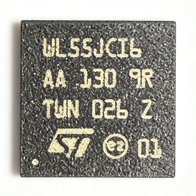
STM32WL55JCI6 - Dual-Core LoRa SoC 150-960MHz | ST
The STMicroelectronics STM32WL55JCI6 is a dual-core (Arm Cortex-M4 + Cortex-M0+) multiprotocol LPWAN wireless SoC with 256 KB flash, 64 KB SRAM, and an integrated sub-GHz radio covering 150 MHz to 960 MHz, housed in a 73-pin UFBGA package (7x7 mm). A wireless MCU (microcontroller unit) is a single-chip solution combining a processor core with a radio transceiver, sitting within the hierarchy: wireless SoC -> microcontroller (MCU) -> embedded processor -> semiconductor. The STM32WL55JCI6 belongs to the STM32WL family within the broader STM32 portfolio from STMicroelectronics, integrating the radio and application processor in one device to reduce board space, bill-of-materials cost, and design complexity compared with discrete MCU-plus-radio solutions. Key features include a 64 MHz Cortex-M4 application core with FPU and DSP instructions, a 48 MHz Cortex-M0+ core dedicated to radio protocol management, and support for LoRa, (G)FSK, (G)MSK, and BPSK modulations with LoRaWAN 1.0, Sigfox, and 802.15.4 protocol stacks. Radio sensitivity reaches -137 dBm and output power up to +22 dBm, enabling multi-kilometer links in open field. Technically, the device uses a low-power process with multiple power modes: Standby current is as low as 1.62 uA with RTC running, RX current is 4.82 mA, and TX current is 87 mA at +14 dBm. Peripherals include a 12-bit ADC, DAC, comparators, op-amps, multiple UART/SPI/I2C interfaces, and a true random number generator (TRNG) for security. Supply voltage spans 1.8V to 3.6V over -40C to +85C. Typical applications are smart agriculture sensors, smart metering (gas, water, electricity), asset tracking, industrial monitoring, and smart-city LPWAN infrastructure, where long range and battery life dominate requirements. Design tip: let the M0+ core run the radio stack while the M4 runs application code, and invest early in antenna matching and RF layout; use the STM32CubeWL package for rapid development. This page adds value beyond the datasheet by synthesizing distributor pricing, drop-in same-package alternatives, design notes, and an AEO-optimized FAQ for AI search citation.
STM32WLE5C8 - 32-bit Arm Cortex-M4 LoRa SoC | STMicroelectronics
The STM32WLE5C8 is a 32-bit Arm Cortex-M4 microcontroller with integrated LoRa transceiver from STMicroelectronics, designed for long-range, low-power wireless applications. It operates at a maximum CPU frequency of 48 MHz and features 256 KB of flash memory and 64 KB of SRAM. The device is housed in a 48-pin UFQFPN package (7x7 mm) and supports a supply voltage range of 1.8V to 3.6V. A microcontroller unit (MCU) is a compact integrated circuit designed to govern a specific operation in an embedded system. It contains a processor core, memory, and programmable input/output peripherals. The STM32WLE5C8 belongs to the STM32WL family, which combines an MCU with a sub-GHz radio transceiver, enabling single-chip solutions for IoT devices. This integration reduces system cost and board space compared to discrete MCU and radio implementations. Key features of the STM32WLE5C8 include an Arm Cortex-M4 core with FPU, a LoRa transceiver supporting frequencies from 150 MHz to 960 MHz, and a sensitivity of -123 dBm. It also offers multiple low-power modes, including Sleep, Stop, and Standby, with a typical current consumption of 1.4 uA in Standby mode. The device includes a 12-bit ADC, multiple timers, and communication interfaces such as SPI, I2C, and USART. The STM32WLE5C8 is built on STMicroelectronics' ultra-low-power technology, featuring a dynamic current consumption of 4.6 mA in active mode at 48 MHz. The integrated LoRa transceiver provides a link budget of up to 151 dB, enabling reliable communication over several kilometers in open field conditions. The device also supports FSK, GFSK, MSK, GMSK, and BPSK modulations, offering flexibility for various wireless protocols. Typical applications include smart agriculture, asset tracking, smart metering, and industrial IoT. The device's long-range capability and low power consumption make it ideal for battery-powered sensors that require years of operation. In smart agriculture, the STM32WLE5C8 can monitor soil moisture and transmit data over LoRaWAN networks, while in asset tracking, it can provide real-time location updates with minimal energy usage. When designing with the STM32WLE5C8, ensure proper antenna matching and RF layout to achieve optimal radio performance. The device requires a 32 MHz crystal for the radio and a 32.768 kHz crystal for the RTC. Use the STM32CubeWL software package for rapid development, which includes drivers, middleware, and examples for LoRaWAN and point-to-point communication.
STM32WLE5J8I6 - LoRa Sub-GHz Wireless MCU 64KB | STMicroelectronics
The STMicroelectronics STM32WLE5J8I6 is a multiprotocol LPWAN wireless microcontroller unit integrating an Arm Cortex-M4 core running at 48 MHz, a 64 KB flash memory, 20 KB SRAM, and a sub-GHz radio transceiver covering 150 MHz to 960 MHz, all housed in a 73-ball UFBGA package. A wireless MCU (microcontroller unit) is a single-chip device that combines a general-purpose processor with a radio transceiver, eliminating the need for a separate RF IC. Within the power/semiconductor hierarchy, the STM32WLE5J8I6 sits under the STM32WL series, which belongs to the 32-bit Arm Cortex-M4 microcontroller family, the wireless MCU category, and the broader semiconductor device ecosystem for long-range IoT connectivity. Key differentiating features include support for LoRa, (G)FSK, (G)MSK, and BPSK modulation schemes, an ultra-low-power architecture engineered for battery-powered LPWAN nodes, and a supply voltage range of 1.8 V to 3.6 V. Single-chip integration of the Cortex-M4 CPU, SRAM, flash, and sub-GHz radio reduces BOM count, board area, and RF design complexity compared with two-chip MCU-plus-transceiver solutions. Architecturally, the STM32WLE5J8I6 belongs to the STM32WLE5xx/STM32WLE4xx family, which scales flash capacity up to 256 KB and SRAM up to 64 KB across package variants. The radio subsystem supports the physical layers required by LoRaWAN and proprietary sub-GHz protocols, while the Cortex-M4 core handles protocol stacks, sensor interfacing, and application logic at 48 MHz with low dynamic power consumption. Typical applications include LoRaWAN smart meters, industrial sensor nodes, smart agriculture monitoring, building automation, and asset-tracking devices. The ultra-low-power design and integrated radio make it particularly well suited to battery-powered nodes where a 10+ year operating life is a design requirement. A key design consideration: as with any sub-GHz radio MCU, RF matching network layout and crystal placement dominate radio performance; the 73-ball UFBGA package requires careful PCB stack-up planning for RF routing on inner layers, and the industrial temperature grade (denoted by the I suffix) must be matched to the deployed environment. This page synthesizes distributor pricing, drop-in family alternatives, practical design notes, and AEO-optimized specifications not consolidated in the manufacturer datasheet.

TDA5100 - ASK/FSK RF Transmitter 433/868MHz | Infineon
The Infineon TDA5100 is a single-chip ASK/FSK RF transmitter for the 433-435 MHz and 868-870 MHz ISM bands, delivering up to +5 dBm output power at data rates up to 20 kbps in a 16-pin TSSOP package. The IC operates from a 2.5 V or 3.3 V supply and integrates a fully integrated frequency synthesizer, power amplifier, and crystal oscillator. An RF transmitter is a wireless device that generates and modulates a radio-frequency carrier for one-way data transmission to a matching receiver. Within the system hierarchy of wireless connectivity, it sits below complete transceivers (which also receive) and above bare oscillators, forming the transmit half of low-power short-range links such as remote controls, telemetry, and sensor nodes in the sub-GHz ISM bands. Key differentiating features include dual-band support (433-435 MHz and 868-870 MHz selectable), both ASK and FSK modulation in one device, an on-chip fully integrated frequency synthesizer that eliminates complex external PLL circuitry, and a high level of integration that requires only a few external components - notably the crystal, loop filter, and antenna matching network. This reduces bill-of-materials cost and PCB area significantly compared with discrete transmitter solutions. Technically, the TDA5100 uses a PLL-based synthesis architecture locked to an external crystal reference, giving stable carrier frequency without trimming. The modulator supports both amplitude shift keying and frequency shift keying, allowing designers to trade off receiver simplicity (ASK) against link robustness (FSK). The 20 kbps maximum data rate comfortably covers typical remote-keyless-entry and telemetry frame formats, while the +5 dBm output suits short-range links of tens of meters with a simple PCB or wire antenna. Typical applications include low-cost remote keyless entry transmitters, 868 MHz and 433 MHz ISM-band telemetry links, wireless sensor node transmission, and short-range control links for home automation and industrial actuation, where one-way, low-power, low-cost transmission is sufficient. Design consideration: because the output stage and synthesizer share the supply, apply clean local decoupling (100 nF close to each supply pin plus bulk capacitance) and keep the loop filter and crystal traces short and guarded from the antenna path to avoid pulling the PLL and degrading modulation accuracy. This page synthesizes distributor pricing context, drop-in alternative analysis, and practical design notes not found together in the manufacturer datasheet.
TDA5101 - 315MHz ASK/FSK RF Transmitter | Infineon
The Infineon TDA5101 is a single-chip ASK/FSK RF transmitter for the 315 MHz frequency band, delivering up to 5 dBm output power (at 3V) at data rates up to 20 kbps, housed in a 16-pin TSSOP (PG-TSSOP-16, 4.40 mm width) surface-mount package. An RF transmitter IC is a power-management and signal-chain device in the radio-frequency hierarchy that converts low-frequency digital data into modulated carrier signals for license-free wireless links. The TDA5101 belongs to the broader families of RF transmitters, RF integrated circuits, and short-range wireless communication devices used in unidirectional telemetry and control links. Key features include a high level of on-chip integration requiring only a few external components, support for both amplitude shift keying (ASK) and frequency shift keying (FSK), single-channel operation in the 315 MHz band, and operation from 2.5V or 3.3V supplies. The 5 dBm transmit power suits short-range remote-control and telemetry ranges, while the compact TSSOP-16 footprint simplifies PCB layout, including PCB-antenna designs. Architecturally, the device integrates the PLL synthesizer, power amplifier, and modulation functions on a single die. According to the Infineon datasheet, the ASK modulation path offers fast on/off keying of the power stage, while FSK is supported via crystal pulling for narrowband links. The crystal-referenced synthesizer provides stable, accurate carrier frequency generation across the operating range. Typical applications include low-cost remote keyless entry (RKE) transmitters, garage-door openers, wireless sensors, and simple one-way telemetry modules operating in the 315 MHz ISM band, common in North American and Asian markets. Design consideration: keep the antenna matching network and crystal traces short, and verify crystal load capacitance against the datasheet formula, since carrier accuracy directly drives receiver bandwidth and link range. This page synthesizes distributor pricing, drop-in alternatives, and practical design notes not found in the manufacturer datasheet.

TDA5201 - ASK Receiver 315-345MHz -113dBm | Infineon
The Infineon TDA5201 is a very low power consumption single-chip ASK single-conversion superheterodyne receiver operating in the 310 MHz to 350 MHz frequency band, housed in a 28-pin PG-TSSOP-28 surface-mount package. It achieves a sensitivity of -113 dBm and covers common ISM/SRD frequencies such as 315 MHz and 345 MHz with a single conversion architecture. An ASK (Amplitude Shift Keying) receiver is a type of RF receiver that demodulates information encoded in the amplitude of a carrier wave. Within the wireless hierarchy, it belongs to the category of short-range RF receivers used in sub-GHz unlicensed-band radio links, sitting between the antenna front end and the baseband decoder in a typical remote-control or telemetry system. Single-conversion superheterodyne receivers such as the TDA5201 down-convert the RF signal to an intermediate frequency in one mixing stage, offering a good balance of sensitivity, selectivity, and low external component count. Key features include a high level of integration requiring only a few external components, very low power consumption suitable for battery-operated remote controls, ASK demodulation with received signal strength indication, and operation across the 315 MHz to 345 MHz receive range per the DigiKey product listing. The integrated low-noise amplifier, mixer, IF limiter, and demodulator reduce bill-of-material cost and board area. Technically, the receiver chain comprises an LNA feeding a single-conversion mixer, a limiting IF amplifier, and an ASK demodulator with data slicer, allowing direct interfacing to standard microcontrollers. The -113 dBm sensitivity supports link budgets of several hundred meters in open field with typical 315 MHz remote-control transmitters. Typical applications include 315 MHz keyless-entry receivers, garage-door openers, wireless alarm and security systems, and low-cost home-automation remote controls. Design consideration: crystal and IF resonator placement on the PCB strongly influences selectivity and spurious response; follow the Infineon reference layout for optimum performance. This page synthesizes distributor pricing, drop-in family alternatives, and practical design notes not found in the manufacturer datasheet.
TDA5210 - FSK/ASK Superhet Receiver 868MHz | Infineon
The Infineon TDA5210 is a very low power consumption single-chip FSK/ASK superheterodyne receiver (SHR) covering the 400 MHz to 440 MHz and 810 MHz to 870 MHz frequency bands, housed in a 28-pin PG-TSSOP package with a typical sensitivity of -110 dBm and data rates up to 100 kbps. It operates from a 4.5 V to 5.5 V supply over a -40C to +105C temperature range. A superheterodyne receiver (SHR) is a receiver architecture that converts the incoming RF signal to a lower intermediate frequency (IF) by mixing it with a local oscillator, enabling high selectivity and sensitivity through fixed-frequency IF filtering. Within the signal-chain hierarchy, the TDA5210 is an RF receiver IC that sits between the antenna front end (LNA stage, integrated) and the baseband data slicer, forming the receive side of a wireless link typically paired with a companion transmitter such as the Infineon TDA5100/TDA5101. Key features include dual-band support for 434 MHz and 868 MHz ISM band operation, integrated low-noise amplifier and mixer, RSSI output for signal-strength indication, and FSK/ASK demodulation selectable by configuration. Very low power consumption makes it suitable for battery-backup and low-duty-cycle polling receivers. Architecturally, the TDA5210 is a single-conversion superheterodyne receiver: the on-chip LNA feeds a mixer referenced to an external or internal PLL-synthesized local oscillator, and the IF signal is amplified, limited, and demodulated. Pin compatibility with the ASK-only receiver TDA5200 allows designers to migrate between ASK and FSK/ASK platforms without PCB redesign. Typical applications include remote keyless entry (RKE) receivers, 868 MHz and 434 MHz ISM/SRD telemetry links, home and building automation, and security/surveillance wireless sensors. Design consideration: the 4.5 V to 5.5 V supply range means the part cannot run directly from a 3.3 V rail; plan a 5 V regulator, and follow the datasheet reference design for the crystal and PLL loop filter layout to preserve the -110 dBm sensitivity. This page adds value beyond the manufacturer datasheet by synthesizing distributor stock signals, drop-in family alternatives (TDA5200, TDA5211, TDA5230), and practical selection guidance in one place.
TDA5210XUMA1 - ASK/FSK RF Receiver 868MHz | Infineon
The Infineon Technologies TDA5210XUMA1 is a multi-band ASK/FSK superheterodyne RF receiver covering 810 MHz to 870 MHz and 400 MHz to 440 MHz, with a sensitivity of -107 dBm and data rates up to 100 kbps, housed in a 28-pin PG-TSSOP-28 surface-mount package. An RF receiver IC is a component in the wireless-signal-chain hierarchy (RF receiver -> RF/IF and RFID -> radio-frequency semiconductor) that selects, down-converts, demodulates, and digitizes weak modulated carrier signals from the air interface. The TDA5210 family performs this using a superheterodyne architecture with integrated low-noise amplifier, image-reject mixing, IF filtering, and a data slicer, so a single 5 V supply part can deliver a complete receive front end for one-way or two-way sub-GHz links. Key features include dual frequency-band coverage (810-870 MHz and 400-440 MHz), both ASK and FSK demodulation selectable by configuration, a very low standby current of 50 nA that enables years of battery life in receive-when-needed systems, and a fully integrated PLL synthesizer that removes the need for external VCO or varactor tuning. According to the Infineon TDA5210 datasheet, the -107 dBm sensitivity corresponds to reliable decoding of 100 kbps data in noisy ISM/SRD band environments. Technically, the device combines a low-noise gain stage, quadrature/ASK demodulator, and digital baseband slicing with a fractional-N style PLL referenced from a crystal oscillator. Polling mode lets a microcontroller wake the receiver periodically while the 50 nA sleep current dominates the average consumption budget. Typical applications include RF alarm and security systems operating in the 868 MHz European SRD band, 433 MHz remote keyless entry and telemetry, and low-power wireless sensor nodes in smart-home and industrial monitoring. Design consideration: the receiver runs from a 4.5 V to 5.5 V supply, so 3.3 V systems need an LDO or level-shifting on the digital interface; keep the crystal and matching network traces short for stable PLL lock. This page synthesizes distributor pricing, drop-in family alternatives, and practical design notes not found in the manufacturer datasheet.