RF Transceivers
Products (74)

AD9082BBCZ - Quad 12GSPS RF DAC & Dual 6GSPS ADC | Analog Devices
The AD9082BBCZ is a highly integrated mixed-signal front-end (MxFE) from Analog Devices, combining a quad, 16-bit, 12 GSPS RF digital-to-analog converter (DAC) core with a dual, 12-bit, 6 GSPS RF analog-to-digital converter (ADC) core. This device supports four transmitter channels and two receiver channels, making it ideal for wideband communication and radar systems. The AD9082 is recommended for new designs and is available in a 324-ball BGA-ED (15x15 mm) package. A mixed-signal front-end (MxFE) is a single-chip solution that integrates high-speed data converters with digital signal processing blocks, enabling direct RF sampling and synthesis. It sits between the analog RF domain and the digital baseband processor, replacing multiple discrete components. The MxFE hierarchy includes RF transceiver -> mixed-signal front-end -> data converter -> semiconductor, streamlining system design and reducing board space. Key features of the AD9082 include a flexible reconfigurable common platform design, supporting 4 DACs and 2 ADCs (4D2A) and 2D2A options. It supports single, dual, and quad band operation, with fully bypassable datapaths and DSP blocks. The device offers DAC to ADC sample rate ratios of 1, 2, 3, and 4, and includes an on-chip PLL with multichip synchronization. These features enable direct RF sampling at frequencies up to 6 GHz for the ADC and 12 GSPS for the DAC, eliminating the need for multiple up/down conversion stages. Technically, the AD9082 integrates a 16-bit DAC core operating at up to 12 GSPS, providing high dynamic range and low noise for transmit paths. The 12-bit ADC core samples at up to 6 GSPS, capturing wideband signals directly at RF frequencies. The on-chip DSP blocks allow for digital up/down conversion, filtering, and gain adjustment, reducing the processing load on the FPGA or ASIC. The device supports JESD204B/C serial interfaces for high-speed data transfer to and from digital processors. Typical applications include 5G NR base stations, phased array radar, electronic warfare, and wideband software-defined radios. The AD9082's ability to handle multiple bands and channels simultaneously makes it suitable for massive MIMO systems and spectrum monitoring. Its high sample rates and direct RF sampling capability reduce system complexity and power consumption compared to traditional heterodyne architectures. When designing with the AD9082, careful attention must be paid to power supply decoupling and thermal management. The device requires multiple supply rails, and proper layout of the high-speed digital and analog interfaces is critical to achieve specified performance. The on-chip PLL requires a clean reference clock, and the JESD204B/C interface must be configured correctly for reliable data transfer.
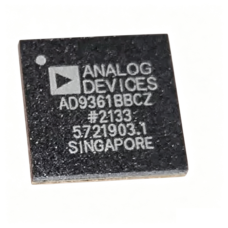
AD9361BBCZ - RF Agile Transceiver 70MHz-6GHz | Analog Devices
The AD9361BBCZ is a high performance, highly integrated radio frequency (RF) Agile Transceiver™ from Analog Devices, designed for 3G and 4G base station applications. It integrates dual transmitters and dual receivers, along with high-performance ADCs, DACs, frequency synthesizers, and digital signal conditioning blocks, into a single 144-ball CSPBGA package. Operating from 70 MHz to 6 GHz, it supports a wide range of wireless standards including LTE, WCDMA, and Wi-Fi. An RF transceiver is a device that combines a transmitter and receiver in a single package, sharing common circuitry. The AD9361 is a specific type of RF transceiver known as an RF Agile Transceiver, which offers wideband frequency coverage and programmability, making it suitable for software-defined radio (SDR) applications. It sits in the hierarchy of RF transceiver -> RF integrated circuit -> analog/mixed-signal IC -> semiconductor. Key features include a 2x2 transceiver architecture with 12-bit ADCs and DACs, a frequency range of 70 MHz to 6 GHz, and support for channel bandwidths from 200 kHz to 56 MHz. The device offers a high level of integration, reducing external component count and board space. It also features a configurable digital interface supporting CMOS and LVDS standards, and a flexible gain control scheme. Technically, the AD9361 uses a direct conversion architecture with integrated synthesizers and filters. It provides excellent linearity and noise performance, with a noise figure of 2 dB in the receive path and an error vector magnitude (EVM) of less than 1% for LTE signals. The device is programmable via a 3-wire or 4-wire SPI interface, allowing dynamic configuration of frequency, gain, and filtering. Typical applications include 3G/4G base stations, software-defined radios, military communications, and test and measurement equipment. Its wideband capability and programmability make it ideal for multi-standard, multi-band radios. The AD9361 is also used in MIMO systems and phased array radar. When designing with the AD9361, careful attention must be paid to power supply decoupling and PCB layout to achieve optimal RF performance. The device requires multiple supply rails, and proper grounding and shielding are essential to minimize noise and interference.

AD9361BBCZ-CSL - RF Agile Transceiver, 70MHz-6GHz | Analog Devices
The AD9361BBCZ-CSL is a high-performance, highly integrated RF Agile Transceiver from Analog Devices, designed for 3G and 4G base station applications. It operates over a frequency range of 70 MHz to 6 GHz and features a 2x2 transceiver architecture with integrated frequency synthesizers, making it ideal for a broad range of radio transceiver applications. The device is housed in a 144-ball CSPBGA package and is qualified for space applications, with radiation testing for Total Ionizing Dose (TID) effects and enhanced reliability for aerospace environments. An RF transceiver is a device that combines a transmitter and receiver in a single package, handling both the modulation/demodulation of signals and the conversion between RF and baseband frequencies. The AD9361BBCZ-CSL integrates the RF front end, mixed-signal baseband, and frequency synthesizers, simplifying design-in and reducing component count. This integration is part of a hierarchy: RF transceiver -> RF front end -> mixed-signal baseband -> frequency synthesizer -> radio communication system. Key features include a wide frequency range of 70 MHz to 6 GHz, support for channel bandwidths from 200 kHz to 56 MHz, and a 12-bit ADC/DAC resolution. The device offers programmable gain control, digital filtering, and a flexible digital interface supporting CMOS and LVDS standards. Its high level of integration eliminates the need for external VCOs and loop filters, reducing board space and design complexity. Technically, the AD9361BBCZ-CSL uses a direct-conversion architecture with integrated fractional-N synthesizers, achieving excellent phase noise and linearity. The device supports both FDD and TDD modes, making it versatile for various wireless standards. Its radiation-hardened design ensures reliable operation in space environments, with TID testing and enhanced screening. Typical applications include 3G/4G base stations, software-defined radios (SDR), military and aerospace communications, and point-to-point microwave links. The wide frequency range and programmability make it suitable for multi-band, multi-standard radios. When designing with this device, careful attention must be paid to power supply decoupling and PCB layout to maintain optimal RF performance. The device requires multiple supply rails and a clean reference clock for best results.
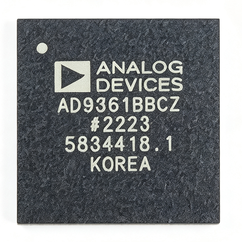
AD9361BBCZ-REEL - 70MHz-6GHz RF Agile Transceiver | Analog Devices
The AD9361BBCZ-REEL is a high performance, highly integrated radio frequency (RF) Agile Transceiver from Analog Devices, designed for 3G and 4G base station applications. It operates over a frequency range of 70 MHz to 6 GHz, covering a wide spectrum of cellular and other wireless standards. The device integrates a 2x2 transceiver architecture with configurable 12-bit CMOS/LVDS digital baseband interface, enabling flexible connection to baseband processors. Housed in a 144-ball CSPBGA package, it offers a compact solution for multi-band, multi-standard radio designs. An RF transceiver is a device that combines both a transmitter and a receiver, sharing common circuitry. The AD9361 is an agile transceiver, meaning it can be dynamically reconfigured to support different frequency bands, channel bandwidths, and modulation schemes. This flexibility makes it a key component in software-defined radio (SDR) systems, where the same hardware can adapt to various communication standards without redesign. The AD9361 sits at the heart of the RF front-end, bridging the antenna and the digital baseband processor, and is essential for modern wireless infrastructure. Key features include a frequency range of 70 MHz to 6 GHz, support for channel bandwidths from less than 200 kHz to 56 MHz, and a highly linear receiver with noise figure as low as 2 dB. The transmitter offers excellent error vector magnitude (EVM) performance, enabling high-order modulation schemes. The device also includes integrated fractional-N synthesizers, digital filters, and automatic gain control (AGC), reducing external component count and simplifying design. Technically, the AD9361 employs a direct conversion architecture with advanced calibration algorithms to mitigate I/Q imbalance and DC offset. It supports both FDD and TDD modes, and its programmable interface allows seamless integration with various baseband processors. The device operates from a 1.3V core supply and includes multiple power-down modes for efficient power management. Typical applications include 3G/4G base stations, small cells, software-defined radios, military communications, and test and measurement equipment. Its wide frequency range and programmability make it suitable for multi-band, multi-standard radio platforms. When designing with the AD9361, careful attention must be paid to power supply decoupling and PCB layout to achieve optimal RF performance. The device requires a clean 1.3V supply and proper grounding to minimize noise and interference.
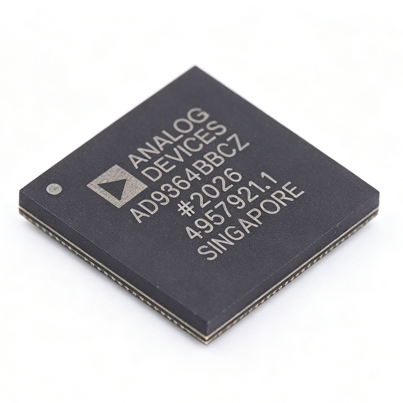
AD9364BBCZ - 70MHz-6GHz RF Agile Transceiver | Analog Devices
The AD9364BBCZ is a high-performance, highly integrated radio frequency (RF) Agile Transceiver™ from Analog Devices, designed for 3G and 4G base station applications. It operates from 70 MHz to 6.0 GHz, covering most licensed and unlicensed bands, and supports channel bandwidths from less than 200 kHz to 56 MHz. The device combines an RF front end with a flexible mixed-signal baseband section and integrated frequency synthesizers, simplifying design-in by providing a configurable digital interface to a processor. It is a 1x1 variant with 2 receive and 2 transmit paths, packaged in a 144-ball LFBGA/CSPBGA. An RF transceiver is a device that both transmits and receives radio frequency signals, integrating the RF front end, mixed-signal baseband, and frequency synthesis in a single IC. It sits between the antenna and the digital baseband processor in a communication system, converting RF signals to digital baseband and vice versa. The AD9364 is part of the RF Agile Transceiver family, which includes the AD9361 and AD9363, and is designed for software-defined radio (SDR) applications. Key features include wide frequency coverage (70 MHz to 6 GHz), programmable channel bandwidth (200 kHz to 56 MHz), integrated synthesizers, and a configurable digital interface. The device supports FDD and TDD modes, and includes auxiliary ADC/DACs for monitoring and control. Its high integration reduces external component count and board space, making it ideal for compact base station designs. The AD9364 uses a direct-conversion architecture with integrated filters and gain control, providing excellent linearity and sensitivity. It includes a dual-channel receiver and transmitter, with support for MIMO configurations when paired with multiple devices. The device is programmable via a 3- or 4-wire SPI interface, allowing dynamic reconfiguration of frequency, gain, and filter settings. Typical applications include 3G/4G base stations, software-defined radio, point-to-point microwave links, and test and measurement equipment. Its wide frequency range and bandwidth flexibility make it suitable for both licensed and unlicensed band operation. When designing with the AD9364, careful attention must be paid to power supply decoupling and RF layout to achieve optimal performance. The device requires multiple supply rails and a clean reference clock. Proper grounding and shielding are essential to minimize noise and interference.
AD9364BBCZ-REEL - 70MHz-6GHz RF Agile Transceiver | Analog Devices
The AD9364BBCZ-REEL is a high-performance, highly integrated RF Agile Transceiver™ from Analog Devices, designed for a broad range of wireless applications. It operates from 70 MHz to 6.0 GHz, covering most licensed and unlicensed bands, and supports channel bandwidths from less than 200 kHz to 56 MHz. The device integrates an RF front end, a flexible mixed-signal baseband section, and frequency synthesizers, simplifying design-in by providing a configurable digital interface to a processor. This 1x1 variant features one receive and one transmit channel, making it ideal for single-channel transceiver designs. An RF transceiver is a device that combines both a transmitter and a receiver in a single package, handling the modulation, demodulation, and frequency conversion of RF signals. It is a critical component in wireless communication systems, bridging the analog RF domain and the digital baseband processor. The AD9364 belongs to the RF Agile Transceiver family, which includes the AD9361 (2x2) and AD9363 (1x1, reduced bandwidth), all sharing a similar architecture and programming model. Key features of the AD9364 include a wide frequency range of 70 MHz to 6 GHz, support for channel bandwidths from 200 kHz to 56 MHz, and a configurable digital interface (CMOS/LVDS) for baseband connectivity. The device offers excellent receiver sensitivity and transmitter linearity, with an output power of 8 dBm. It also includes integrated fractional-N synthesizers, reducing external component count and simplifying frequency planning. Technically, the AD9364 employs a direct-conversion architecture with advanced calibration algorithms to minimize I/Q imbalance and DC offset. The device supports both FDD and TDD modes, making it versatile for various wireless standards. Its programmability allows dynamic reconfiguration of frequency, bandwidth, and gain, enabling software-defined radio (SDR) implementations. Typical applications include 3G/4G base stations, software-defined radios, portable test equipment, and military communications. The wide frequency range and bandwidth flexibility make it suitable for multi-standard radios that must operate across different bands. When designing with the AD9364, careful attention must be paid to power supply decoupling and clocking. The device requires multiple supply rails, and proper filtering is essential to achieve optimal performance. The digital interface should be configured for the appropriate voltage levels and data rate to match the baseband processor.
AD9371BBCZ - Dual RF Transceiver 300MHz-6GHz | Analog Devices
The AD9371BBCZ is a highly integrated, wideband RF transceiver from Analog Devices, designed for dual-channel transmitters and receivers with integrated synthesizers and digital signal processing functions. It operates over a frequency range of 300 MHz to 6 GHz, making it suitable for a wide variety of wireless applications. The device is packaged in a 196-ball LFBGA/CSPBGA (12 mm x 12 mm) and is part of the Mykonos family. An RF transceiver is a device that combines both a transmitter and a receiver in a single package, enabling bidirectional communication over radio frequencies. The AD9371 is a system-on-chip (SoC) that integrates the RF front-end, analog-to-digital converters (ADCs), digital-to-analog converters (DACs), and digital signal processing (DSP) blocks, reducing the need for external components and simplifying system design. It sits within the hierarchy of RF transceivers -> wideband transceivers -> software-defined radio (SDR) components. Key features include dual transmitters and receivers, support for TDD and FDD modes, and a digital interface that supports JESD204B serial data. The device offers high dynamic range and low power consumption, making it ideal for battery-powered and portable applications. It also includes an observation path for transmitter monitoring and calibration, enhancing system performance. Technically, the AD9371 integrates fractional-N synthesizers for local oscillator (LO) generation, reducing external LO circuitry. The device supports a maximum receiver bandwidth of 100 MHz and transmitter bandwidth of 250 MHz, enabling wideband operation. It operates from a 3.3V supply and includes power management features to optimize efficiency. Typical applications include software-defined radios, cellular base stations (3G/4G/5G), point-to-point microwave links, and military communications. Its wide frequency range and high integration make it a versatile choice for both commercial and defense systems. When designing with the AD9371, careful attention must be paid to power supply decoupling and thermal management, as the device dissipates significant power. The JESD204B interface requires proper clocking and synchronization to ensure data integrity.
AD9371BBCZ-REEL - Dual RF Transceiver 300MHz-6GHz | Analog Devices
The AD9371BBCZ-REEL from Analog Devices is a highly integrated, wideband RF transceiver designed for dual-channel transmitters and receivers, integrated synthesizers, and digital signal processing functions. Operating from 300 MHz to 6 GHz, this device supports a wide range of wireless communication standards, including 4G/5G cellular infrastructure, software-defined radio (SDR), and radar systems. The transceiver is housed in a 196-ball CSP_BGA package (12 mm × 12 mm), offering a compact solution for high-performance RF front-ends. An RF transceiver is a device that combines both a transmitter and a receiver in a single package, handling the modulation, demodulation, and frequency conversion of RF signals. In the hierarchy of wireless communication systems, an RF transceiver sits between the baseband processor and the antenna, converting digital baseband data to analog RF signals for transmission and vice versa for reception. The AD9371 integrates dual transmitters and receivers, along with observation and feedback paths, enabling advanced features like digital pre-distortion (DPD) and envelope tracking. Key features of the AD9371 include dual-channel transmitters and receivers, integrated synthesizers, and a digital signal processing block that supports various filtering and calibration functions. The device offers a high dynamic range and low noise figure, making it suitable for demanding applications. It also includes an observation receiver (ORx) path for DPD and a feedback path for transmit monitoring. The transceiver supports a wide frequency range, from 300 MHz to 6 GHz, covering most cellular and ISM bands. Technically, the AD9371 employs a direct-conversion architecture with advanced calibration algorithms to achieve high performance. It integrates fractional-N synthesizers for both transmit and receive paths, reducing external component count. The device operates from a 1.3 V core supply and 1.8 V I/O supply, with power dissipation typically around 5 W. The digital interface supports JESD204B, a high-speed serial interface standard, enabling efficient data transfer to FPGAs or ASICs. Typical applications include 4G/5G macro and small cell base stations, software-defined radios, phased array radar, and test and measurement equipment. The AD9371's wide frequency range and high integration make it ideal for multi-band, multi-standard systems where board space and power efficiency are critical. When designing with the AD9371, careful attention must be paid to power supply decoupling and thermal management. The device requires multiple supply rails, and proper filtering is essential to achieve the specified noise performance. The exposed pad on the CSP_BGA package should be soldered to a thermal via array to ensure adequate heat dissipation.
AD9375BBCZ - Dual RF Transceiver with DPD | Analog Devices
The AD9375BBCZ is a highly integrated, wideband radio frequency (RF) transceiver from Analog Devices, designed for 3G/4G/5G base stations and massive MIMO systems. It features dual-channel transmitters (Tx) and receivers (Rx), integrated synthesizers, a fully integrated digital predistortion (DPD) actuator and adaptation engine, and comprehensive digital signal processing functions. Operating from 300 MHz to 6 GHz, it supports a wide range of cellular and wireless standards. An RF transceiver is a device that combines both a transmitter and a receiver in a single package, sharing common circuitry. In the hierarchy of wireless communication systems, an RF transceiver is a key component within the RF front-end, which sits between the antenna and the baseband processor. It handles the conversion of RF signals to and from intermediate frequencies or baseband, enabling wireless communication. The AD9375 is a high-performance example, integrating DPD to enhance linearity and efficiency in power amplifiers. Key features include dual-channel operation, integrated DPD, and a frequency range of 300 MHz to 6 GHz. The device supports observation paths for DPD and includes digital signal processing functions such as filtering, gain control, and calibration. It is housed in a 196-ball LFBGA/CSPBGA package, suitable for compact base station designs. The integrated DPD engine reduces the need for external DPD components, simplifying system design and reducing bill of materials. Technically, the AD9375 uses a direct conversion architecture with high dynamic range and linearity. It includes multiple PLLs and synthesizers for flexible frequency planning. The DPD actuator and adaptation engine work together to correct power amplifier nonlinearities, improving system efficiency and reducing spectral regrowth. The device also supports MIMO configurations, making it ideal for advanced antenna systems. Typical applications include 3G/4G/5G base stations, massive MIMO systems, software-defined radios, and military communications. Its wide frequency range and DPD capability make it suitable for both FDD and TDD systems. When designing with the AD9375, careful attention must be paid to power supply decoupling and thermal management. The device requires multiple supply rails and a well-designed PCB layout to achieve optimal performance. The integrated DPD engine requires configuration and calibration, which can be done via the serial peripheral interface (SPI).
AD9375BBCZ-REEL - Dual RF Transceiver with DPD | Analog Devices
The AD9375BBCZ-REEL is a highly integrated, dual RF transceiver from Analog Devices, designed for cellular and wireless infrastructure applications. It operates over a frequency range of 300 MHz to 6 GHz, covering a wide spectrum of communication bands. The device integrates two independent transmit and receive channels, along with an observation path for digital predistortion (DPD) and a sniffer receiver for spectrum monitoring. It is housed in a 196-ball LFBGA/CSPBGA package, offering a compact solution for multi-band, multi-standard transceiver designs. An RF transceiver is a device that combines both a transmitter and a receiver in a single package, handling the modulation, demodulation, and frequency conversion of RF signals. In modern communication systems, RF transceivers are essential components in base stations, small cells, and other wireless infrastructure, enabling high-speed data transmission and reception. The AD9375 belongs to the family of wideband transceivers, which are characterized by their ability to handle multiple frequency bands and communication standards, such as LTE, 5G NR, and WCDMA, with a single hardware platform. Key features of the AD9375 include its wide frequency range, dual-channel architecture, and integrated DPD capability. The DPD functionality allows for linearization of power amplifiers, improving efficiency and reducing distortion. The device also features a high dynamic range, with a receiver noise figure of [DATA_NEEDED: receiver noise figure] and a transmitter error vector magnitude (EVM) of [DATA_NEEDED: transmitter EVM]. It supports a maximum bandwidth of [DATA_NEEDED: maximum bandwidth] per channel, making it suitable for carrier aggregation and high-throughput applications. Technically, the AD9375 is built on a highly integrated architecture that includes mixers, filters, ADCs, DACs, and digital signal processing blocks. It uses a direct conversion architecture for both transmit and receive paths, minimizing external components and simplifying the design. The device is controlled via a serial peripheral interface (SPI), allowing for flexible configuration of frequency, gain, and filtering. It also includes a digital interface for baseband data transfer, supporting JESD204B standard for high-speed serial data transmission. Typical applications for the AD9375 include 4G/5G base stations, small cells, massive MIMO systems, and software-defined radios. Its wide frequency range and high performance make it ideal for multi-band, multi-standard transceivers, reducing the need for multiple discrete components. The integrated DPD capability is particularly beneficial in power amplifier linearization, improving system efficiency and reducing power consumption. When designing with the AD9375, it is important to consider the power supply requirements and thermal management. The device requires multiple supply rails, including 1.3V and [DATA_NEEDED: other supply voltages], and dissipates significant power, especially when operating at high output power. Proper PCB layout, including adequate grounding and decoupling, is critical to achieve optimal performance. Additionally, the JESD204B interface requires careful attention to clocking and synchronization to ensure reliable data transfer.
ADAR1000 - 8-16GHz 4-Channel Beamformer | Analog Devices
The ADAR1000 is a 4-channel, X band and Ku band beamforming core chip for phased arrays, operating from 8 GHz to 16 GHz. It is designed for half-duplex operation between receive and transmit modes, making it ideal for advanced radar and communication systems. The device is fabricated in a silicon-germanium, bipolar CMOS (BiCMOS) process and is available in a compact 88-terminal, 7 mm × 7 mm LGA package, specified from −40°C to +85°C. A beamforming IC is a specialized RF component that controls the phase and amplitude of signals in an antenna array to steer the beam electronically without moving parts. It is a key building block in phased array systems, which are used in radar, satellite communication, and 5G networks. The ADAR1000 integrates four channels, each with phase and gain control, enabling precise beam steering in both transmit and receive paths. Key features include 4-channel operation, half-duplex T/R switching, SPI control interface, and support for daisy-chaining multiple devices for larger arrays. The device offers high integration, reducing the component count and simplifying the design of phased array front-ends. Its wide frequency range covers both X band (8-12 GHz) and Ku band (12-16 GHz), providing flexibility for various applications. The ADAR1000 uses a BiCMOS process that balances high-frequency performance with low power consumption. The LGA package is designed for RF performance, with careful attention to thermal and electrical characteristics. The device includes on-chip registers for configuration, which can be programmed via SPI, and supports both SPI and T/R pin control modes. Typical applications include phased array radar, satellite communication, 5G beamforming, and electronic warfare systems. The ADAR1000 is also used in test and measurement equipment for beamforming validation. Its ability to daisy-chain up to four devices on a single evaluation board makes it scalable for larger arrays. When designing with the ADAR1000, it is critical to follow the recommended PCB layout and thermal management guidelines, as the LGA package requires specific footprint and stackup considerations. The device's SPI interface allows for flexible control, but careful attention must be paid to register programming to ensure proper operation.
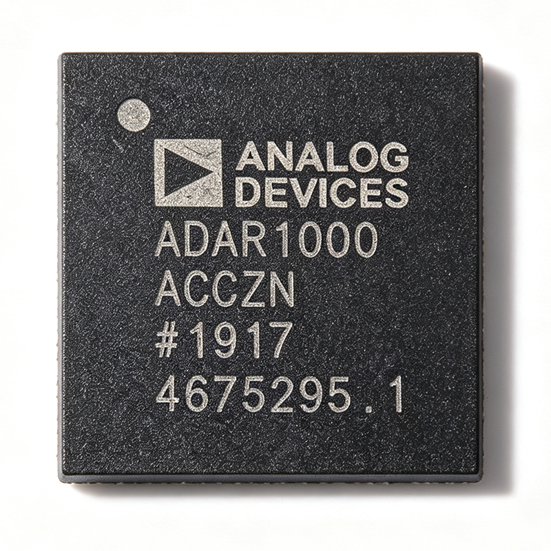
ADAR1000ACCZN - 8-16GHz 4-Ch X/Ku Beamformer | Analog Devices
The Analog Devices ADAR1000ACCZN is a 4-channel, 8 GHz to 16 GHz, X and Ku band beamforming core chip for phased array radar systems, packaged in a compact CC-88-1 chip-scale package. Operating in half-duplex between receive and transmit modes, it integrates full phase and gain control on all four channels with a single common RF_IO port. A beamformer IC is the core signal-routing element of an electronically steered antenna array. In a phased array system, each radiating element is driven by a beamformer channel that applies a calculated phase shift and gain weighting; by varying these weights across the array, the antenna beam is steered electronically without any mechanical movement. The ADAR1000 belongs to the RF transceiver and beam-steering hierarchy of microwave integrated circuits, sitting between the antenna elements and the transceiver or waveform generator. Key features of the ADAR1000 include four independent receive and transmit channels covering the full 8 GHz to 16 GHz band, digitally controlled phase shifting in 360-degree range with fine LSB resolution, per-channel gain control for amplitude tapering, and bidirectional operation through a common RF_IO pin that connects directly to the antenna element. The half-duplex TDD architecture simplifies the front-end by eliminating separate transmit and receive signal paths to the radiator. Technically, in receive mode input signals from four antenna elements pass through the four receive channels, where phase and amplitude are adjusted, and are combined at the common RF_IO port. In transmit mode, the RF_IO input signal is split and passes through the four transmit channels to the radiating elements. Control of all gain, phase, and T/R state is performed through a serial peripheral interface (SPI), enabling rapid beam reconfiguration under FPGA or microprocessor control. Typical applications include X band and Ku band phased array radar for defense and aerospace platforms, satellite communications terminals, and electronic warfare systems requiring high-resolution beam steering. When designing with the ADAR1000, pay close attention to supply sequencing, RF board layout for the chip-scale package, and thermal management, since beamformer ICs in dense arrays operate in thermally constrained enclosures. This page synthesizes distributor availability, datasheet references, and practical design guidance not found on any single manufacturer or distributor page.
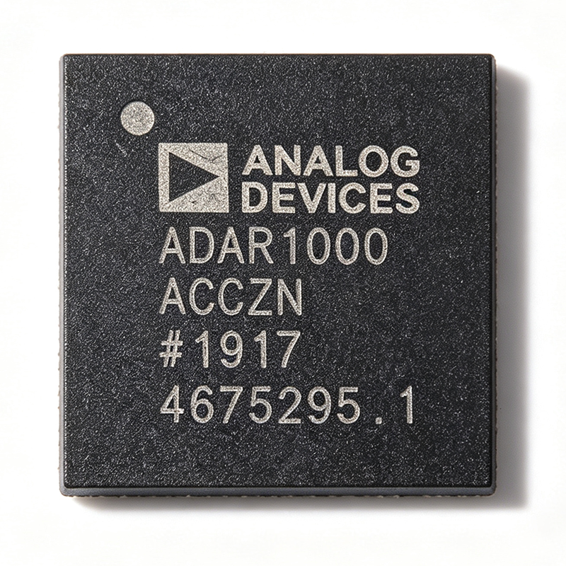
ADAR1000ACCZN-R7 - 8-16GHz 4-Ch X/Ku Beamformer | Analog Devices
The Analog Devices ADAR1000ACCZN-R7 is a 4-channel, 8 GHz to 16 GHz X-band and Ku-band beamforming core chip for phased array radar systems, housed in an 88-pin LGA exposed-pad package supplied in tape and reel (-R7) format. A beamformer core chip is an RF integrated circuit that provides independent amplitude and phase control per channel, enabling electronic steering of a phased array antenna without mechanical movement. Within the RF signal chain hierarchy, the ADAR1000 sits between the transceiver and the antenna elements, functioning as the vector-modulating T/R module that shapes the beam. Beamformers like the ADAR1000 are foundational building blocks of modern active electronically scanned array (AESA) architectures used in radar and communication systems. Key features include 4 fully independent receive and transmit channels covering 8 GHz to 16 GHz, half-duplex operation with fast transmit/receive switching controlled by a single pin, and per-channel programmable phase and gain. The device integrates the complete beamforming function - low noise amplification in receive mode, power amplification in transmit mode, and vector modulation on every channel - reducing board area and component count dramatically versus discrete implementations. Architecturally, in receive mode input signals pass through the four receive channels and are combined at the common RF_IO pin; in transmit mode the RF_IO input signal is split and passes through the four transmit channels. All on-chip registers are controlled through a simple 4-wire serial port interface (SPI), and two address pins allow SPI control of up to four ADAR1000 devices on the same serial lines, simplifying large array designs. Dedicated transmit and receive load pins provide synchronization of all ADAR1000 chips in the same array. Typical applications include X-band and Ku-band phased array radar, satellite communication terminals, and multi-beam antenna systems where compact size, precise phase/gain control, and channel-to-channel synchronization are required. Design consideration: because the four channels share the common RF_IO port, PCB symmetry between channels is important for maintaining amplitude and phase tracking across the array. This page synthesizes distributor availability data, packaging details, and application guidance not consolidated in the manufacturer datasheet alone.

ADL5385ACPZ - 30MHz-2.2GHz Quadrature Modulator | Analog Devices
The ADL5385ACPZ is a silicon, monolithic, quadrature modulator designed for use from 30 MHz to 2200 MHz. It is housed in a 24-lead LFCSP (lead frame chip scale package) with an exposed pad, providing excellent thermal and electrical performance. The device takes signals from two differential baseband inputs and modulates them onto two carriers in quadrature, enabling high-performance intermediate frequency (IF) and direct radio frequency (RF) modulation for communication systems. A quadrature modulator is a key building block in modern communication transmitters, converting baseband I/Q signals into a modulated RF output. It is essential for digital modulation schemes such as QPSK, QAM, and OFDM, which are widely used in wireless standards including LTE, Wi-Fi, and point-to-point microwave links. The ADL5385's excellent phase accuracy and amplitude balance ensure minimal error vector magnitude (EVM), which is critical for high data-rate links. Key features of the ADL5385ACPZ include a wide operating frequency range of 30 MHz to 2200 MHz, high output linearity, and low noise. The device operates from a single 5 V supply and features a differential baseband interface with a common-mode voltage of approximately 2.5 V. It provides a differential RF output that can be used with an external balun to convert to single-ended. The modulator also includes an enable function for power-down control, reducing quiescent current when not in use. Technically, the ADL5385 uses a double-balanced mixer architecture with integrated quadrature phase splitting. The LO input is internally divided into I and Q phases, and each is mixed with the corresponding baseband signal. The outputs are summed to produce the modulated RF signal. The device achieves high sideband suppression and carrier feedthrough performance, which are essential for spectral purity. The baseband inputs accept a wide common-mode range, simplifying interface to DACs and baseband processors. Typical applications include cellular base stations, microwave point-to-point radios, satellite communications, and test equipment. The ADL5385 is also suitable for software-defined radio (SDR) transmitters where flexibility and performance are paramount. Its wide frequency range covers multiple bands, reducing the need for multiple modulators. When designing with the ADL5385ACPZ, ensure proper grounding and decoupling of the supply pins. The exposed pad should be soldered to a low-impedance ground plane for optimal thermal and RF performance. The baseband inputs should be driven with differential signals to maintain balance and minimize even-order distortion.
ADL5385ACPZ-R7 - 50MHz-2.2GHz Quadrature Modulator | Analog Devices
The ADL5385ACPZ-R7 is a silicon, monolithic, quadrature modulator designed for use from 30 MHz to 2200 MHz. It is housed in a 24-lead LFCSP (WFQFN) package with an exposed pad, and is supplied in tape and reel packaging. This device provides excellent phase accuracy and amplitude balance, enabling high performance intermediate frequency (IF) and direct radio frequency (RF) modulation for communication systems. A quadrature modulator is a key building block in modern wireless transmitters. It takes two baseband signals (I and Q) and modulates them onto a carrier signal, producing a modulated RF output. This architecture is fundamental to digital communication standards such as WCDMA, LTE, and WiMAX, where complex modulation schemes require precise I/Q balance. The ADL5385 simplifies the design of such transmitters by integrating the modulator function into a single IC, reducing component count and board space. Key features of the ADL5385 include a wide operating frequency range from 30 MHz to 2200 MHz, excellent phase accuracy and amplitude balance, and a differential baseband interface. The device operates from a single 5V supply and provides a high output IP3, making it suitable for demanding linearity requirements. The LFCSP package with exposed pad ensures efficient thermal dissipation, while the tape and reel packaging (R7 suffix) is optimized for high-volume production. Technically, the ADL5385 uses a double-balanced mixer topology with integrated quadrature phase splitting. This architecture provides high carrier feedthrough suppression and excellent sideband suppression, which are critical for spectral purity. The device also features a wide baseband bandwidth, allowing it to support both narrowband and wideband modulation schemes. Its performance is specified over the full -40°C to +85°C temperature range, ensuring reliable operation in diverse environments. Typical applications include cellular base stations, point-to-point radios, satellite communications, and test and measurement equipment. In these systems, the ADL5385 is used to upconvert baseband I/Q signals to RF frequencies, enabling efficient and accurate signal transmission. Its high linearity and low noise make it ideal for high-performance communication links. When designing with the ADL5385, it is important to provide proper decoupling on the supply pins and to match the differential baseband inputs to the driving source impedance. The exposed pad should be soldered to a ground plane for optimal thermal and electrical performance. Additionally, the LO input should be driven with a clean, well-leveled signal to achieve the best carrier feedthrough performance.
ADMV1013S-CSL - 24-44GHz Upconverter | Analog Devices
The ADMV1013S-CSL is a wideband, microwave upconverter from Analog Devices, designed for point-to-point microwave radio systems operating in the 24 GHz to 44 GHz frequency range. It comes in a compact, thermally enhanced 40-terminal land grid array (LGA) package and operates over a case temperature range of -40°C to +85°C. This device is part of the Commercial Space Products Program, offering enhanced reliability for space and high-reliability applications. A microwave upconverter is a critical component in RF transmitters that translates a lower intermediate frequency (IF) signal to a higher radio frequency (RF) for transmission. In the hierarchy of RF signal chains, the upconverter sits between the baseband/modem and the power amplifier, converting the modulated IF signal to the desired RF band. The ADMV1013S-CSL supports two modes of frequency translation, providing flexibility in system architecture. Key features include wideband operation from 24 GHz to 44 GHz, which covers multiple microwave bands including K and Ka bands. The device offers high linearity and low conversion loss, essential for maintaining signal integrity in high-order modulation schemes. The LGA package provides excellent thermal performance, enabling reliable operation in demanding environments. The -40°C to +85°C case temperature range ensures suitability for both commercial and space-grade applications. Technically, the ADMV1013S-CSL integrates a double-balanced mixer, local oscillator (LO) buffer, and RF amplifier in a single package. This integration reduces external component count and simplifies board design. The device is optimized for point-to-point microwave links, where frequency stability and phase noise are critical. The upconverter's wideband nature allows it to be used across multiple frequency plans without redesign. Typical applications include 5G mmWave infrastructure, satellite communications, radar systems, and test and measurement equipment. In 5G base stations, the ADMV1013S-CSL can upconvert IF signals to the 24-44 GHz band for massive MIMO and beamforming arrays. For satellite ground terminals, it provides reliable frequency conversion for Ka-band links. When designing with this device, ensure proper impedance matching at all ports and provide adequate grounding for the LGA package. The thermal pad should be connected to a solid ground plane with thermal vias to maximize heat dissipation. Also, consider the LO drive level and isolation to prevent spurious emissions.

ADMV4821 - 24-29.5GHz 5G Beamformer | Analog Devices
The ADMV4821 is a highly integrated silicon germanium (SiGe) beamformer from Analog Devices, operating over the 24 GHz to 29.5 GHz frequency range. It addresses the n257, n258, and n261 5G NR bands in a single footprint, supporting 16 selectable transmit (TX) and 16 selectable receive (RX) channels. The device provides both horizontal and vertical polarization through independent RFV and RFH common pins, enabling dual-polarized antenna arrays. It is packaged in a compact LGA package that allows top-side heatsinking for efficient thermal management and flexible antenna placement on the opposite side of the PCB. A beamformer is a key component in phased-array antenna systems, responsible for adjusting the phase and amplitude of signals to steer the antenna beam electronically without moving parts. In 5G mmWave base stations, beamformers enable massive MIMO (Multiple-Input Multiple-Output) configurations, improving spectral efficiency and coverage. The ADMV4821 integrates 16 channels, each with independent phase and gain control, into a single IC, significantly reducing the size and complexity of the RF front-end compared to discrete implementations. Key features include a wide operating frequency range covering multiple 5G bands, 16 TX and 16 RX channels, dual polarization support, and a serial peripheral interface (SPI) for control. The device operates over a -40°C to +95°C case temperature range, making it suitable for outdoor base station environments. The LGA package with top-side heatsinking allows for efficient heat dissipation, crucial for high-power beamforming applications. The ADMV4821 uses a SiGe process technology, offering a good balance of performance and integration for mmWave frequencies. The SPI interface enables precise control of phase and gain settings, with a protocol consisting of a read/write bit, 15 register address bits, and 8 data bits. The device includes internal LDO regulators, allowing it to be powered from a single supply, simplifying power supply design. Typical applications include 5G NR base stations, phased-array antennas, satellite communications, and radar systems. In 5G base stations, the ADMV4821 is used in the active antenna unit to form and steer beams, improving signal quality and capacity. Its dual-polarization capability supports polarization diversity, enhancing link reliability. When designing with the ADMV4821, careful attention must be paid to thermal management, as the device can dissipate significant power. The LGA package's top-side heatsinking should be utilized with an appropriate heatsink or thermal interface material. Additionally, the SPI interface should be properly terminated and decoupled to ensure reliable control.
ADMV4821B - 24-29.5GHz Dual-Pol Beamformer | Analog Devices
The ADMV4821B is a dual-polarization beamformer from Analog Devices, operating over the 24 GHz to 29.5 GHz frequency range, covering the n257, n258, and n261 5G NR bands in a single footprint. It integrates 16 selectable transmit (TX) channels and 16 selectable receive (RX) channels, supporting horizontal and vertical polarization with matched 50-ohm single-ended RF inputs and outputs. This device is designed for phased-array antenna systems in 5G base stations and satellite communications, offering high integration to simplify beamforming architectures. A beamformer is a key component in phased-array systems that electronically steers the antenna beam by adjusting the phase and amplitude of signals across multiple antenna elements. The ADMV4821B belongs to the class of RF beamforming ICs, which are essential in modern 5G NR and radar systems. By integrating multiple channels and dual polarization, it reduces the component count and PCB area compared to discrete implementations, enabling compact and cost-effective antenna modules. Key features include a wide RF frequency range of 24 GHz to 29.5 GHz, 16 TX and 16 RX channels, dual polarization support, and matched 50-ohm single-ended interfaces. The device is recommended for new designs, indicating active lifecycle status. It is packaged in a compact BCCZ package, suitable for surface-mount assembly, and is designed to meet the stringent performance requirements of 5G infrastructure. Technically, the ADMV4821B integrates phase shifters, gain amplifiers, and T/R switches on a single die, providing precise beam control. The dual-polarization capability allows simultaneous transmission and reception on both horizontal and vertical polarizations, doubling the data throughput in MIMO systems. The device is controlled via a serial interface, enabling fast beam steering and calibration. Typical applications include 5G NR base stations, phased-array antennas, satellite communications, and radar systems. Its wide frequency coverage and dual-polarization support make it ideal for massive MIMO and beamforming networks. The device's high integration reduces system complexity and power consumption, making it suitable for dense antenna arrays. When designing with the ADMV4821B, careful attention must be paid to thermal management and RF layout. The device's thermal resistance values are simulated based on JEDEC specifications (JESD51-12), so proper PCB design with adequate ground vias and heat sinking is critical. Additionally, the RF inputs and outputs are single-ended 50-ohm, requiring proper impedance matching to minimize reflections.
ADMV4821C - 24-29.5GHz Dual-Pol Beamformer | Analog Devices
The ADMV4821C is a dual-polarization beamformer from Analog Devices, operating from 24 GHz to 29.5 GHz, covering the n257, n258, and n261 5G NR bands in a single footprint. It integrates 16 selectable TX channels and 16 selectable RX channels, supporting both horizontal and vertical polarization. The device features matched 50-ohm single-ended RF inputs and outputs, simplifying system integration. It is recommended for new designs and is available in a compact BCCZ package, suitable for phased-array antenna systems. A beamformer is a key component in phased-array antenna systems, responsible for controlling the phase and amplitude of signals to steer the antenna beam electronically. It is part of the RF front-end chain, which includes antennas, transceivers, and beamformers. The ADMV4821C is a dual-polarization beamformer, meaning it can handle both horizontal and vertical polarizations simultaneously, effectively doubling the data throughput in MIMO systems. This makes it ideal for 5G base stations and satellite communications. Key features include a wide RF frequency range of 24 GHz to 29.5 GHz, 16 TX and 16 RX channels, dual-polarization support, and matched 50-ohm single-ended interfaces. The device is designed for high linearity and low noise figure, ensuring excellent signal quality. It also offers flexible control interfaces for beam steering, making it suitable for advanced antenna arrays. Technically, the ADMV4821C integrates multiple RF chains with phase shifters and gain amplifiers, all controlled via a serial interface. The dual-polarization architecture allows for 2x2 MIMO operation, enhancing spectral efficiency. The device operates from a single supply voltage and includes on-chip temperature compensation for stable performance across temperature. Typical applications include 5G NR base stations, satellite ground terminals, radar systems, and point-to-point communication links. The wide frequency coverage and dual-polarization capability make it a versatile solution for emerging mmWave applications. When designing with the ADMV4821C, careful attention must be paid to thermal management and RF layout. The device dissipates significant power, and proper heat sinking is essential. Additionally, the RF traces should be impedance-matched to 50 ohms to minimize reflections.

ADRV9002BBCZ - Dual RF Transceiver 30MHz-6GHz | Analog Devices
The ADRV9002BBCZ is a highly integrated, dual-channel RF transceiver from Analog Devices, designed for a wide range of wireless applications. It operates from 30 MHz to 6 GHz, covering HF, VHF, UHF, and microwave bands. The device integrates dual transmitters, dual receivers, synthesizers, and digital signal processing functions, providing a complete radio solution in a compact 196-ball CSPBGA package (12x12 mm). An RF transceiver is a device that combines both a transmitter and a receiver in a single package, enabling bidirectional communication over a radio frequency link. The ADRV9002 is a high-performance, highly linear, high dynamic range transceiver, making it suitable for demanding applications such as software-defined radio (SDR), 5G NR, and military communications. It supports both narrowband and wideband operation, offering flexibility for various system architectures. Key features include dual-channel operation, frequency coverage from 30 MHz to 6 GHz, and integrated digital signal processing. The device provides excellent linearity and dynamic range, essential for modern communication systems. It operates over a temperature range of -40°C to +110°C, ensuring reliability in harsh environments. The package is a 196-TFBGA, CSPBGA, with a supplier device package of 196-CSPBGA (12x12). The ADRV9002 utilizes advanced RF CMOS technology, integrating multiple functions that traditionally required discrete components. This integration reduces board space, power consumption, and system cost. The device includes on-chip synthesizers and digital filtering, simplifying the design of RF front-ends. Its high dynamic range enables it to handle weak signals in the presence of strong interferers, a critical requirement in crowded spectrum environments. Typical applications include software-defined radio, 5G NR base stations, point-to-point microwave links, and military communications. The wide frequency range and dual-channel capability make it ideal for MIMO and diversity systems. The device is also suitable for test and measurement equipment, where precise RF signal generation and analysis are required. When designing with the ADRV9002, careful attention must be paid to power supply decoupling and thermal management. The device's power dissipation is significant, and proper PCB layout with adequate ground planes and thermal vias is essential. The evaluation board EVAL-ADRV9002 provides a reference design for optimal performance.

ADRV9002BBCZ-REEL - Dual RF Transceiver 30MHz-6GHz | Analog Devices
The ADRV9002BBCZ-REEL is a highly integrated, dual-channel RF transceiver from Analog Devices, designed for both narrow-band and wideband applications. It operates over a frequency range of 30 MHz to 6 GHz, making it suitable for a wide variety of wireless communication systems. The device integrates dual-channel transmitters, dual-channel receivers, synthesizers, and digital signal processing functions in a compact 196-ball TFBGA/CSPBGA package. This tape-and-reel variant is optimized for high-volume production. An RF transceiver is a device that combines both a transmitter and a receiver in a single package, sharing common circuitry. The ADRV9002 is a system-on-chip (SoC) that integrates the RF front-end, analog-to-digital converters (ADCs), digital-to-analog converters (DACs), and digital signal processing (DSP) blocks. This level of integration reduces component count, board space, and design complexity, making it ideal for software-defined radios (SDR) and other advanced wireless systems. Key features of the ADRV9002 include dual-channel operation, a wide frequency range of 30 MHz to 6 GHz, and support for both narrow-band and wideband signals. The device offers high linearity and dynamic range, ensuring reliable performance in demanding environments. It also includes integrated synthesizers, reducing the need for external PLLs and VCOs. The power output is 7.8 dBm, and the device operates from a single 3.3V supply. The ADRV9002 uses advanced CMOS technology to achieve high performance with low power consumption. The digital signal processing functions include filtering, gain control, and calibration, which are configurable via a serial peripheral interface (SPI). The device supports multiple operating modes, including TDD and FDD, and can be programmed for various bandwidths and sample rates. The integrated synthesizers provide low phase noise, essential for high-quality signal transmission and reception. Typical applications for the ADRV9002 include 5G NR base stations, small cells, macro cells, and other wireless infrastructure. It is also used in military and aerospace communications, radar systems, and test and measurement equipment. The wide frequency range and dual-channel capability make it a versatile choice for many RF designs. When designing with the ADRV9002, careful attention must be paid to power supply decoupling and thermal management. The device requires a clean 3.3V supply and adequate grounding to achieve optimal performance. The exposed pad on the package should be soldered to a thermal via array to dissipate heat effectively.
ADRV9003BBCZ - 1x1 RF Transceiver 30MHz-6GHz | Analog Devices
The ADRV9003BBCZ is a highly integrated, single-channel RF transceiver from Analog Devices, designed for a wide range of wireless applications. It operates from 30 MHz to 6 GHz, covering HF, VHF, UHF, and microwave bands, and features a single-channel transmitter, dual-channel receivers, integrated synthesizers, and extensive digital signal processing functions. The device is housed in a 196-pin CSP-BGA package, making it suitable for compact, high-performance designs. An RF transceiver is a device that combines a transmitter and a receiver in a single package, sharing common circuitry. It is a fundamental building block in wireless communication systems, enabling bidirectional data transfer over radio frequencies. The ADRV9003 integrates the RF front-end, analog-to-digital converters (ADCs), digital-to-analog converters (DACs), and digital signal processing, reducing the need for external components and simplifying system design. Key features of the ADRV9003 include a wide frequency range of 30 MHz to 6 GHz, a maximum sample rate of 61.44 MSPS, and high linearity and dynamic range. The device supports both FDD and TDD operation, making it versatile for various communication standards. It also includes integrated synthesizers and a digital interface, allowing for flexible configuration and control. The ADRV9003 utilizes advanced mixed-signal technology, integrating multiple functions that traditionally required separate components. Its architecture enables high performance while minimizing power consumption and board space. The device is designed for applications such as 5G base stations, software-defined radios, and test and measurement equipment, where high performance and flexibility are critical. Typical applications include 5G wireless infrastructure, point-to-point microwave links, and military communications. The wide frequency range and high dynamic range make it suitable for demanding environments. The device's integrated DSP functions allow for real-time signal processing, reducing the load on external processors. When designing with the ADRV9003, careful attention must be paid to power supply decoupling and thermal management. The device requires multiple supply rails, and proper filtering is essential to achieve optimal performance. The CSP-BGA package requires a well-designed PCB layout with adequate thermal vias to dissipate heat effectively.
ADRV9003BBCZ-REEL - 30MHz-6GHz RF Transceiver | ADI
Analog Devices ADRV9003BBCZ-REEL is a highly integrated RF transceiver covering 30 MHz to 6 GHz, with a single-channel transmitter, dual-channel receivers, integrated synthesizers, and extensive digital signal processing functions. The device is supplied on tape and reel for high-volume surface-mount assembly and is part of the ADRV900x family used in wireless infrastructure and defense radio systems. The antenna is not included, so external antenna circuitry is required. An RF transceiver is a combined transmitter and receiver used in radio systems to convert between baseband digital data and modulated RF signals. In an ADRV9003-class transceiver, integrated synthesizers generate local-oscillator signals, while on-chip DSP performs filtering, gain control, calibration, and data formatting before handoff to an FPGA or SoC. This integration replaces multiple discrete IF/RF components and shortens radio design cycles. Key features of the ADRV9003BBCZ-REEL include the 30 MHz to 6 GHz operational range, 1T2R channel architecture, high linearity, high dynamic range, integrated synthesizers, and digital signal processing capabilities. According to the ADI product page, the device is optimized for high performance in demanding communications links. From an architecture perspective, the 1T2R configuration suits TDD systems that need one transmit path and two receive paths, such as base stations with receive diversity or dual-direction monitoring. The integrated DSP offloads many radio functions from the baseband processor, reducing host FPGA resource usage and supporting multiband software-defined radios. Typical applications include 5G/4G small cells, software-defined radios, phased-array radar feeds, industrial IoT gateways, satellite communications, and test-and-measurement instruments. In these systems, the device's bandwidth and linearity reduce error vector magnitude (EVM) and improve sensitivity. When designing with the ADRV9003BBCZ-REEL, pay attention to board-level thermal management for the BGA package and clean supply filtering near the RF pins. A well-controlled RF layout with proper impedance matching and grounding is essential to achieve the high dynamic range promised by the datasheet.
ADRV9004BBCZ - Dual RF Transceiver 30MHz-6GHz | Analog Devices
The ADRV9004BBCZ is a highly integrated, dual-channel RF transceiver from Analog Devices, designed for narrow-band and wideband applications. It operates over a frequency range of 30 MHz to 6 GHz, covering HF, VHF, UHF, and microwave bands. The device integrates dual-channel transmitters, dual-channel receivers, integrated synthesizers, and digital signal processing functions into a single 196-ball CSP_BGA package (12 mm × 12 mm). It supports configurable CMOS or LVDS serial synchronous interfaces (SSI) for high and low data rate communication. An RF transceiver is a device that combines a transmitter and receiver, sharing common circuitry or a single housing. In the hierarchy of wireless communication systems, an RF transceiver is a key component within the radio frequency front-end, which connects the antenna to the baseband processor. The ADRV9004BBCZ is a software-defined radio (SDR) solution, enabling flexible modulation schemes and frequency agility through digital control. Key features include dual-channel operation, wide frequency coverage, high linearity, and high dynamic range. The device supports both narrow-band and wideband signal processing, making it suitable for a variety of communication standards. It operates with 1.3V and 1.8V power supplies, and is available in a tray packaging. The ADRV9004BBCZ is RoHS compliant and is an active product in Analog Devices' portfolio. Technically, the ADRV9004BBCZ integrates multiple synthesizers, mixers, filters, and ADCs/DACs, providing a complete RF front-end solution. Its digital signal processing capabilities include filtering, gain control, and calibration algorithms, reducing the need for external components. The device is designed for high performance, with excellent noise figure and linearity, ensuring reliable communication in demanding environments. Typical applications include cellular base stations, point-to-point microwave links, satellite communications, and defense systems. Its wide frequency range and dual-channel capability make it ideal for MIMO and diversity schemes. The compact package and integrated functionality reduce board space and design complexity. When designing with the ADRV9004BBCZ, careful attention must be paid to power supply decoupling and thermal management. The device's thermal resistance values are specified per JEDEC standards (JESD51-12), and proper PCB layout with adequate ground planes is essential for optimal RF performance.