Clock Generators
بەرهەمەکان (3)

ADF4372BCCZ-RL7 - 16 GHz Integer-N PLL Synthesizer | Analog Devices
Analog Devices ADF4372BCCZ-RL7 is an integer-N phase-locked-loop frequency synthesizer with an integrated voltage-controlled oscillator, a maximum output frequency of 16 GHz, and a 48-lead TFLGA package with an exposed pad. Its VCO fundamental range extends from 4 GHz to 8 GHz, while programmable RF outputs cover 62.5 MHz to 16 GHz. A phase-locked loop, or PLL, synchronizes an output oscillator to a stable reference frequency. The ADF4372 integrates the VCO and synthesizer circuitry into one RF device, allowing a reference oscillator and external loop filter to define a phase-locked output. Its integer-N architecture avoids the fractional-N spur and phase-noise behavior associated with fractional dividers, making it suitable for coherent RF systems requiring predictable spectral content. The device supports RF division by 1, 2, 4, 8, 16, 32, or 64. This allows the 4 GHz to 8 GHz VCO fundamental to be divided down to outputs as low as 62.5 MHz at RF8x. A frequency multiplier provides an 8 GHz to 16 GHz range at RF16x, and RFAUX8x provides an auxiliary output at the eighth-divider frequency. As an integer-N synthesizer, the ADF4372 provides a single programmable output path rather than independent fractional and integer divider systems. The implementation requires an external reference and loop filter. Loop-filter component values determine reference-to-output multiplication ratio, bandwidth, phase noise, and transient behavior, so the reference frequency and target channel spacing must be considered together during design. Typical applications include microwave and millimeter-wave radio front ends, instrumentation, test and measurement equipment, radar-related signal generation, and wideband communication modules. The 16 GHz maximum output supports Ku-band and related RF systems, while the broad divided-output range allows the same synthesizer to support lower-frequency receiver and test circuits. PCB implementation requires careful treatment of the exposed thermal pad, supply connections, RF outputs, and high-speed reference signals. The exposed pad must be connected to the ground plane with adequate thermal-via density, and the external loop filter should be positioned to minimize sensitive RF and feedback-trace coupling. This page combines the ADF4372 frequency ranges, output architecture, package information, sourcing guidance, replacement considerations, and practical PCB-design guidance into a compact engineering reference for evaluating the ADF4372BCCZ-RL7 in integer-N RF synthesizer designs.
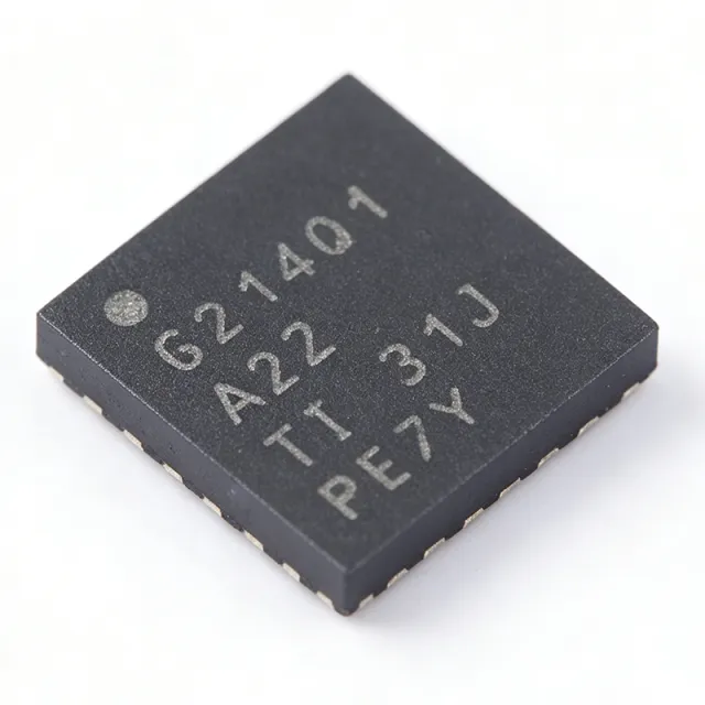
CDCE6214TWRGERQ1 - Ultra-Low Power Clock Generator | TI
The CDCE6214TWRGERQ1 is an automotive-grade, ultra-low power clock generator from Texas Instruments, designed to support PCIe Gen 1-5 with two inputs, four differential outputs, and internal EEPROM. It integrates one fractional-N PLL and can generate five independent clock outputs selectable between various driver modes. The device operates from a 3.3V supply and is packaged in a 24-pin VQFN (4mm x 4mm) with exposed pad, making it suitable for space-constrained automotive and industrial applications. A clock generator is a semiconductor device that produces one or more clock signals from a reference input, typically using a phase-locked loop (PLL) to multiply or divide frequencies. It is a fundamental building block in digital systems, providing timing signals for processors, interfaces, and data converters. Clock generators are part of the broader category of timing and synchronization ICs, which also includes clock buffers, jitter cleaners, and frequency synthesizers. Key features include ultra-low power consumption, medium-grade jitter performance, and a configurable high-performance low-power fractional-N PLL. The device supports I2C-compatible interface up to 400kHz, integrated EEPROM with two pages and an external select pin, and in-situ programming. It also supports 100Ω systems and offers low electromagnetic emissions. The small 24-pin VQFN footprint (4mm x 4mm) enables compact designs. Technically, the CDCE6214-Q1 uses a fractional-N PLL architecture that allows precise frequency synthesis with low spurious content. The RMS jitter with spurs (12kHz - 20MHz, Fout > 100MHz) is specified for integer and fractional modes, ensuring reliable operation in high-speed serial links. The device is AEC-Q100 qualified for automotive applications, meeting stringent reliability and temperature requirements. Typical applications include advanced driver assistance systems (ADAS), automotive infotainment, and industrial automation where multiple clock domains are required. The device can generate clocks for PCIe, Ethernet, and other high-speed interfaces, providing a single-chip solution for clock tree generation. When designing with this device, ensure proper power supply decoupling with 0.1uF and 1uF capacitors close to the VDD pins. The EEPROM can be programmed in-situ via I2C, allowing flexible configuration without external programming hardware. Consider the output driver modes to match the load requirements and minimize signal integrity issues.
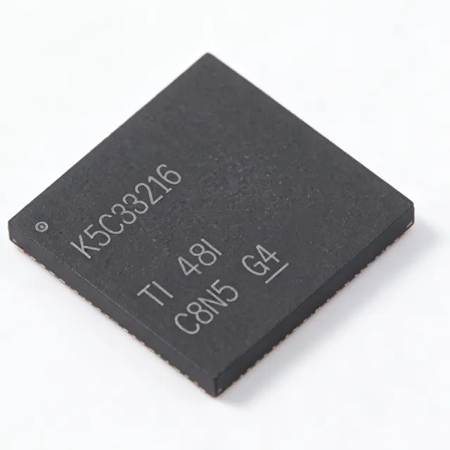
LMK5C33216RGCR - Ultra-Low Jitter Clock Synchronizer | TI
The Texas Instruments LMK5C33216RGCR is an ultra-low jitter clock synchronizer, jitter attenuator, and clock generator designed for wireless communications infrastructure. It integrates three high-performance digital phase-locked loops (DPLLs) with paired analog phase-locked loops (APLLs) and a BAW (Bulk Acoustic Wave) APLL that achieves 40 fs RMS jitter at 491.52 MHz. The device supports output frequencies up to 3 GHz and operates from a 3.3V supply in a 64-pin VQFN (RGC) package with exposed thermal pad. A clock synchronizer is a specialized timing IC that generates and aligns multiple clock signals to a reference, often cleaning jitter from noisy sources. In the hierarchy of timing components, a clock synchronizer sits above a simple PLL or clock generator, providing advanced features like hitless switching, holdover, and digital loop filtering. The LMK5C33216 is part of TI's LMK5C family, which targets 5G base stations, small cells, and other high-speed networking equipment where precise timing is critical for JESD204B data converters. Key features include three DPLLs with programmable loop bandwidth from 0.01 Hz to 4 kHz, eliminating the need for external loop filters. The BAW APLL delivers exceptional jitter performance of 40 fs RMS, while the device also offers -116 dBc/Hz phase noise at 100 Hz offset. It supports JESD204B interface for direct connection to high-speed ADCs and DACs, and includes advanced reference clock selection with hitless switching to maintain synchronization during reference failures. The LMK5C33216 integrates a flexible clock output architecture with multiple dividers and delays, allowing generation of various frequencies from a single reference. Its digital PLL architecture provides precise frequency synthesis and alignment, while the analog PLLs ensure low-noise output. The device is programmable via SPI or I2C, enabling dynamic reconfiguration in the field. Typical applications include 5G NR base stations, remote radio heads, small cells, and test and measurement equipment. The device is also suitable for optical transport networks and data center switches requiring high-frequency, low-jitter clocks. Its wide output frequency range and low jitter make it ideal for JESD204B converter clocking. When designing with the LMK5C33216, ensure proper power supply decoupling with low-ESR capacitors close to the VQFN pins. The exposed thermal pad must be soldered to a ground plane for adequate heat dissipation. Use the device's internal loop filters to simplify design, but verify loop bandwidth settings for your specific jitter transfer requirements.