Logic ICs
بەرهەمەکان (720+)

SY58051AUMG-TR - 10.7Gbps CML AnyGate Logic | Microchip
The Microchip Technology SY58051AUMG-TR is an ultra-fast, low-jitter universal CML logic gate (AnyGate) with a guaranteed maximum data throughput of 10.7 Gbps or clock throughput of 8 GHz, housed in a 16-pin QFN (3x3 mm) package with exposed pad. It operates from a 2.3 V to 3.465 V supply (2.5 V and 3.3 V nominal) across -40C to +85C. A universal logic gate is a differential high-speed gate that can be configured to realize many Boolean functions of two variables, such as AND, OR, NAND, NOR, XOR, and XNOR, by strapping or biasing its inputs. Within the signal-chain hierarchy it sits in the logic IC family alongside gates and inverters, but unlike standard CMOS logic it is built on a precision CML (current-mode logic) architecture optimized for multi-gigabit serial links rather than for static power savings. Key features include differential CML inputs and outputs with internal input and output termination, eliminating external resistor-bias and termination networks; a VT pin that exposes the input termination network for easy AC- or DC-coupled interfacing to multiple logic standards (LVPECL, LVDS, CML); and picosecond-class jitter performance suitable for SONET, Fibre Channel, and 10 Gigabit Ethernet timing budgets. The internal termination design produces a clean, stub-free interface, reducing reflections and jitter contributions at the package boundary. Because termination is integrated, board designers save the discrete resistor networks typically required at 10 Gbps, improving signal integrity and layout density. The exposed-pad QFN-16 provides a low-inductance ground return essential for CML switching at multi-gigahertz edge rates. Typical applications include 10G Ethernet and Fibre Channel retiming paths, clock distribution and gating in high-speed test equipment, logic gating in optical module signal chains, and protocol translation between CML, LVDS, and LVPECL domains. A key design consideration: the VT pin must be biased correctly for the chosen logic standard and coupling mode; AC-coupled CML and DC-coupled LVDS each require different VT configurations per the manufacturer datasheet. This page synthesizes distributor pricing, drop-in alternatives, pinout guidance, and practical design notes not found in the manufacturer datasheet.

TCA39306DDFR - Dual I2C/I3C Bidirectional Level Translator | TI
The Texas Instruments TCA39306DDFR is a 2-bit dual bidirectional voltage-level translator compatible with I2C, SMBus, and I3C (up to 12.5 MHz), operating from a 0.9 V to 3.3 V VREF1 rail and a 1.8 V to 5.5 V VREF2 rail, housed in an 8-pin TSOT-23-8 (DDF) surface-mount package. A voltage-level translator (also called a logic level shifter or voltage translator) is an integrated circuit that allows digital signals referenced to one supply domain to drive inputs in a different supply domain. Within the system hierarchy, level translators sit in the logic and interface IC family, bridging mismatched voltage domains between microcontrollers, sensors, and peripherals. Bidirectional translators such as the TCA39306 are essential for open-drain buses like I2C, where the same two wires (SDA and SCL) carry traffic in both directions. Key features include automatic bidirectional translation without a direction pin, support for Standard-mode (100 kbps), Fast-mode (400 kbps), and Fast-mode Plus (1 Mbps) I2C, plus I3C compatibility at 12.5 MHz, and an enable (EN) input for bus isolation. The low ON-state resistance (RON) of the internal pass-gate switches minimizes signal degradation and bus loading. Technically, the TCA39306 implements the reference-voltage biased switch architecture: VREF1 biases one side of the pass gate and VREF2 the other, so the open-drain pull-up levels define the translated logic levels. This pass-switch topology draws negligible static current and preserves I3C push-pull signaling on the SDA line, which open-drain-only solutions cannot support. Typical applications include mixed-voltage I2C bus segments (for example, a 1.8 V sensor side talking to a 3.3 V or 5 V controller side), SMBus systems in servers and power supplies, and emerging I3C peripherals in mobile and IoT designs. The tiny TSOT-23-8 footprint suits space-constrained board layouts. Design consideration: choose pull-up resistors on both sides appropriately - lower-value pull-ups (for example 1 kOhm to 4.7 kOhm) are needed for Fast-mode Plus and I3C rise-time compliance, while the EN pin can be driven to isolate the bus during reset sequences. This page synthesizes distributor pricing, drop-in alternative analysis, and practical design notes not found in the manufacturer datasheet.

TCA39306DTMR - Dual I2C/SMBus/I3C Bidirectional Level Translator | TI
The Texas Instruments TCA39306DTMR is a dual (2-bit) bidirectional voltage-level translator for SDA and SCL lines in mixed-voltage I2C, SMBus, and I3C applications, supporting VREF1 from 0.9V to 3.3V, VREF2 from 1.8V to 5.5V, and translations between 0.85V and 5V, housed in an 8-pin X2SON (1.35mm x 0.8mm) package with tape-and-reel delivery. A voltage-level translator is a logic-family interface IC that bridges digital signals between circuits operating at different supply rails, a member of the broader voltage-translation and logic-translation hierarchy within standard logic ICs. For open-drain buses such as I2C and SMBus, a bidirectional translator is required because data flows both ways on the same line without a direction-control pin; the TCA39306 solves this by using pass-gate switches with integrated pull-up references tied to each side's reference voltage. Key features include standard-mode (100 kbps), fast-mode (400 kbps), and fast-mode-plus (1 Mbps) I2C compatibility, I3C compatibility up to 12.5 MHz, an enable (EN) input for power sequencing and bus isolation, and very low ON-state resistance (RON) of the internal switches, which minimizes signal attenuation and allows external pull-up resistors to remain small. Because there is no direction pin, both channels (SDA and SCL) translate automatically as the bus arbitrates. Technically, the device uses two NMOS pass transistors per channel: when B-side is high, the switch conducts and the A-side tracks it; when A-side is pulled low, the switch passes the low level through. The EN pin must be driven to VREF1 for normal operation and can be grounded to place the bus in high-impedance, useful for hot-swapping and multi-master isolation. Typical applications include mixed-voltage MCU-to-sensor I2C links, server and industrial automation bus translation, and consumer electronics peripheral interfaces where a 1.8V controller must talk to a 3.3V or 5V peripheral. Design consideration: choose pull-up resistors for both rails carefully; smaller pull-ups speed rising edges but increase sink current through the internal switch, so follow the TI TCA39306 EVM User's Guide (SCPU045) guidance on load capacitance and pull-up selection. This page synthesizes distributor pricing context, drop-in alternative analysis, and practical design notes that go beyond the manufacturer datasheet.

TCA9406DCTR - 2-Bit Bidirectional I2C/SMBus Level Translator | TI
The Texas Instruments TCA9406DCTR is a 2-bit bidirectional I2C bus and SMBus voltage-level translator with an output enable (OE) input, operational from 1.65 V to 3.6 V on the A-side (VCCA) and 2.3 V to 5.5 V on the B-side (VCCB), housed in an 8-pin SM8/SSOP surface-mount package with 8 kV HBM ESD protection. A voltage-level translator is an interface IC that bridges digital signal domains operating at different supply rails, allowing a microcontroller running at 1.8 V or 3.3 V to safely communicate with peripheral devices on a 5 V bus. Within the signal-chain hierarchy, level translators sit between logic ICs and physical bus lines and are essential members of the I2C/SMBus interface family, where open-drain bidirectional lines cannot be shifted with simple resistor dividers. Key differentiating specifications include true bidirectional operation without a direction pin, support for the 1-MHz Fast-mode Plus I2C class of operation with data rates up to 24 Mbps in general-purpose push-pull use, and 8 kV human-body-model ESD robustness on the bus pins. The dedicated OE input lets the system place both channels in the high-impedance state during power sequencing or bus reconfiguration, preventing bus contention and back-powering through partial-rail conditions. Architecturally, the TCA9406 integrates an internal boost/reference generator on the B side so that only two supply pins (VCCA and VCCB) and a minimal external component count are required - no external pull-up resistors to a reference rail are needed, unlike pass-gate translators such as the TI PCA9306. This integrated drive makes rise and fall times far less dependent on bus loading, which matters when the bus runs at 400 kHz or 1 MHz with cable or connector capacitance. Typical applications include I2C sensor interfacing in battery-powered products, SMBus communication between 3.3 V management controllers and 5 V power-supply modules, and level shifting between low-voltage MCUs and 5 V EEPROMs or RTCs. It fits anywhere a 1.8 V, 2.5 V, or 3.3 V host must drive a 5 V peripheral bus reliably. A key design consideration: the OE pin should be driven by a supply-rail supervisor or held low until both VCCA and VCCB are stable, since enabling the translator before the higher rail is up can momentarily clamp the bus. This page synthesizes distributor pricing and stock, drop-in alternative analysis against the NXP PCA9306, pinout data, and practical design notes not found in the manufacturer datasheet.
TLV3801 - 225ps LVDS High-Speed Comparator | Texas Instruments
The Texas Instruments TLV3801 is a 225-ps high-speed comparator with complementary LVDS outputs, operating from a single 2.7 V to 5.25 V supply or a split supply of ±1.35 V to ±2.625 V, with a toggle frequency up to 3 GHz. It is packaged in an 8-pin WSON (DSG) 2x2 mm package for space-constrained designs. A comparator is an electronic circuit that compares two input voltages and outputs a digital signal indicating which is larger. The TLV3801 belongs to the high-speed comparator subclass, optimized for minimal propagation delay and high toggle rates. It sits within the analog-to-digital interface hierarchy, bridging analog signals to LVDS digital logic levels for downstream FPGAs and CPUs. Key features include a 225-ps propagation delay, complementary LVDS outputs that reduce EMI and suppress common-mode noise, and low power consumption of about 6.5 mW at 3.3 V. An enable pin supports power management and rail sequencing. The LVDS output stages drive standard LVDS inputs directly at up to 3 GHz toggle frequency. The device is built on a bipolar process with a differential input stage and LVDS output drivers, delivering deterministic, low-jitter switching. It is specified over the industrial temperature range of -40C to +125C, and an automotive-grade TLV3801-Q1 variant is available for AEC-Q100 applications. Typical applications include LIDAR pulse detection, where every nanosecond of propagation delay affects range resolution, high-speed differential line receivers for data transmission, and optical sensor modules. Clock recovery and fast data acquisition systems also benefit from the high toggle rate. Design tip: terminate the LVDS outputs with 100 ohm differential impedance and decouple each supply pin with 0.1 uF capacitors placed as close to the device as possible to preserve signal integrity.

TMUX8108PWR - 100V Flat RON 8:1 Analog MUX | Texas Instruments
The Texas Instruments TMUX8108PWR is a 100-V rated, flat on-resistance, single 8:1 (single-ended) analog multiplexer housed in a 16-pin TSSOP (PWR) package. It delivers a consistent on-resistance of approximately 50 ohm across the full analog signal range and supply conditions, supports single, dual, or asymmetric supplies up to 100 V total, and features latch-up immunity plus 1.8-V-compatible logic inputs. An analog multiplexer is a switching IC that routes one of several analog signal inputs to a single common output under digital control, forming part of the broader family of analog switches within signal-chain and power-management integrated circuits. Multiplexers are essential wherever many sensors, test points, or signal sources share a single downstream amplifier, ADC, or measurement instrument, saving board area, cost, and channel count on data converters. Key differentiating features of the TMUX8108 include its 100-V maximum supply rating, far above the 36 V ceiling of conventional CMOS multiplexers, its flat RON characteristic that minimizes signal-dependent gain error across the signal range, and latch-up immunity that protects the device in harsh industrial and medical environments where voltage transients are common. Control logic accepts 1.8 V, 3.3 V, and 5 V levels and, according to TI product documentation, logic inputs can be driven as high as 48 V, giving designers exceptional flexibility in interfacing with mixed-voltage systems. The device supports bidirectional analog and digital signals on the source (Sx) and drain (D) pins and provides break-before-make switching to prevent momentary channel shorting. Consistent analog parametric performance is maintained across the entire supply voltage range, simplifying design reuse from low-voltage to high-voltage systems. Typical applications include industrial programmable logic controller analog input modules, battery test and formation equipment, medical diagnostic instrumentation front ends, and automated test equipment (ATE) signal routing, all of which benefit from the high supply ceiling and rugged latch-up immunity. Designers should observe the total supply constraint of 100 V across VDD and VSS and verify signal swing stays within the supply rails; the flat RON makes channel-to-channel matching predictable even at high common-mode voltages. This page synthesizes verified distributor data, drop-in alternatives, and practical design guidance not found in the manufacturer datasheet, with pricing referenced as of 2026-09-03.

TMUX8108RUMR - 100V 8:1 Analog Mux, 48Ohm | Texas Instruments
The Texas Instruments TMUX8108RUMR is a 100 V, flat RON, single 8:1 analog multiplexer with latch-up immunity and 1.8 V logic compatibility, housed in a 16-pin WQFN (4x4 mm, RUM) package with a typical on-resistance of 48 ohm. An analog multiplexer is a switching IC that routes one of several analog input signals to a single output channel under digital control. Within the signal-chain hierarchy, it sits between sensors or signal sources and amplifiers, ADCs, or measurement front ends, acting as a electronically controlled switch matrix. Multiplexer ICs belong to the broader family of analog switches, which themselves are part of the interface and signal-routing layer of power and data acquisition systems. Key features of the TMUX8108 include support for dual, single, or asymmetric supplies up to a maximum supply voltage of 100 V, low and flat on-capacitance behavior across the signal range, low OFF leakage current, and robust latch-up immunity that protects the device in harsh industrial environments. The 1.8 V-compatible logic inputs allow direct interfacing with modern low-voltage microcontrollers and FPGAs without level shifting. Technically, the TMUX810x family provides consistent analog parametric performance across the entire supply voltage range, meaning RON, leakage, and switching behavior remain stable whether the part runs from plus/minus supplies or a single high-voltage rail. This flat RON characteristic minimizes signal-dependent gain error in precision measurement paths, a common weakness of older high-voltage mux architectures. Typical applications include industrial programmable logic controller (PLC) analog input modules, automated test equipment (ATE) signal routing, battery test and formation systems operating at high cell voltages, and high-voltage data acquisition front ends. The 8:1 configuration suits multi-channel monitoring where several sense points share one precision ADC. A key design consideration is supply configuration: because the device accepts up to 100 V total supply, designers should verify signal swing stays within the supply rails and account for on-resistance times channel-current voltage drops in error budgets. This page synthesizes distributor pricing, drop-in alternative analysis, and practical design notes not found in the manufacturer datasheet, giving engineers a complete selection resource in one place.

TMUXHS4446RETR - USB-C 10Gbps Alt Mode Crossbar Mux | Texas Instruments
The Texas Instruments TMUXHS4446RETR is a high-speed bidirectional passive crosspoint switch (crossbar/Xbar) that switches USB 3.2 Gen2 SuperSpeed and DisplayPort 1.4/2.1 signals up to 10Gbps UHBR10 over a USB Type-C interface, housed in a 40-pin WQFN (6x3 mm) package with a typical on-resistance of 7 ohm. A crosspoint switch, also called a crossbar mux, is a type of analog signal switch that can route any of its input lanes to any of its output lanes in a non-blocking matrix fashion. Within the signal-routing hierarchy, it sits above simple SPDT analog switches and USB 2:1 muxes, offering full lane-level flexibility for multi-protocol interfaces. Crossbar muxes are key building blocks of USB-C Alternate Mode systems, where a single reversible connector must carry either USB SuperSpeed data or DisplayPort video depending on negotiation. Key features include support for 10Gbps data rates compliant with USB 3.2 Gen2 and DisplayPort UHBR10, a passive switch architecture that adds no signal retiming or protocol awareness, integrated switching for the low-speed SBU (Sideband Use) lines used by the DisplayPort auxiliary channel, and a 7-ohm typical on-resistance that minimizes insertion loss. The 4-circuit, 4:4 configuration maps directly onto the four SuperSpeed differential lane pairs of a USB-C connector. The passive, bidirectional architecture means the device does not distinguish between source and sink: signals pass equally well in either direction, simplifying orientation and role handling in USB-C designs. Wide, flat differential lanes are laid out inside the WQFN-40 to maintain controlled impedance and low crosstalk at multi-gigabit speeds. Typical applications include USB-C docking stations, laptop and tablet USB-C Alternate Mode ports, USB-C monitors and display adapters, and multi-function hubs that multiplex USB 3.2 Gen2 and DisplayPort 1.4/2.1 over the same connector. Design consideration: at 10Gbps, keep the passive high-speed lanes short, impedance-controlled, and decoupled from the switching-control logic; insertion loss and via stubs matter more than with low-speed muxes. This page synthesizes distributor pricing, package data, application guidance, and design notes not found in a single manufacturer datasheet.

TPS3701DDCR - 36V Window Comparator | Texas Instruments
The Texas Instruments TPS3701DDCR is a 36 V window voltage comparator with an internal 400 mV reference, two open-drain outputs, and a 1.8 V to 36 V supply range, packaged in a 6-pin SOT-23-THIN. It monitors overvoltage and undervoltage conditions in industrial, embedded, and power-management systems. The two precision comparators can operate together as a window detector or independently as two voltage monitors, while external resistors set the monitored thresholds. A window comparator is a specialized voltage-monitoring IC that compares an input voltage against programmed upper and lower limits. Unlike a simple power-supply supervisor, this device combines two precision comparators, a low-power 400 mV reference, and separate fault outputs. It belongs to the broader hierarchy of comparator, voltage supervisor, power-management IC, and semiconductor categories. Its open-drain outputs can pull fault lines or enable signals low and may be wired for wired-AND behavior when required by the system architecture. Key features include a wide 1.8 V to 36 V supply operating range, thresholds adjustable down to 400 mV, low typical quiescent current of 7 microamperes, and high threshold accuracy. The outputs, identified as OUTA and OUTB, are rated to 25 V for overvoltage and undervoltage signaling. The monitored voltage is established with external resistor networks, allowing the same device to address different system rails without changing the comparator package. The TPS3701 architecture is useful when a system must distinguish a valid operating window from an unsafe condition. Two open-drain outputs provide separate information for undervoltage and overvoltage events, helping a controller, protection circuit, or system-management block respond without interpreting a single ambiguous fault signal. The internal reference improves repeatability when the monitored rail is divided down to the reference range. Typical applications include industrial control systems, embedded power rails, battery-powered equipment, power-supply sequencing, automotive-style voltage supervision, and general overvoltage or undervoltage protection. The 36 V supply capability is useful for systems whose monitored rails exceed conventional low-voltage logic levels, while the open-drain outputs allow flexible pull-up selection and interface-level adaptation. When designing the circuit, verify the external resistor divider limits, open-drain pull-up voltage, monitored-voltage range, and output timing before connecting the device. The 6-pin SOT-23-THIN package requires careful placement and adequate copper area. Because the outputs are open-drain, each line needs an appropriate pull-up unless it is intentionally connected to another open-drain node. This page combines manufacturer specifications, distributor availability information, application guidance, and verified replacement analysis. It is intended to help engineers identify whether the TPS3701DDCR fits a voltage-window monitoring design and to distinguish genuine same-footprint replacements from parts that only provide similar monitoring functions.

TPS3701DDCT - 36V Dual Window Comparator | Texas Instruments
The Texas Instruments TPS3701DDCT is a dual window voltage detector with two precision comparators, a 400 mV internal reference, and two open-drain outputs rated to 25 V, packaged in a 6-pin SOT-23-THIN configuration. It operates from 1.8 V to 36 V and is designed for overvoltage and undervoltage monitoring. A window comparator is a voltage detector that checks whether an input voltage lies between programmable upper and lower thresholds. Unlike a general-purpose comparator, this device integrates two comparison channels and a reference, allowing one IC to monitor both rail boundaries. In the power-management hierarchy, it belongs to the comparator and voltage-supervisor family rather than a power-regulator family. Key features include the 1.8 V to 36 V supply range, a 400 mV internal reference, two open-drain outputs, and monitoring flexibility through external resistor networks. The open-drain outputs can be pulled up to an appropriate external voltage, allowing wired interface use and flexible system-level signaling. Reported low quiescent current is approximately 7 µA typical, making the device suitable for low-power monitoring systems. The TPS3701 can operate as a window detector or as two independent voltage monitors. The monitored thresholds are established with external resistors, while the internal reference provides the comparison basis. Its high-voltage operating range allows monitoring of industrial supplies and other rails where input transients or nominal voltages exceed the range of simpler low-voltage supervisors. Response time is reported in distributor data as approximately 155 µs. Typical applications include industrial automation, battery systems, power-supply protection, sensor interfaces, and embedded control systems. It is especially useful when a system must assert separate fault signals when a monitored voltage becomes too high or too low. Because the outputs are open-drain, pull-up resistors are required unless the output is connected directly to a compatible pull-up arrangement. Designers should verify the full datasheet pinout, threshold tolerances, timing, output ratings, and capacitor or resistor recommendations before production. The SOT-23-THIN footprint supports compact layouts, but the open-drain pins and monitor-input network require careful routing. For replacements, compare the complete pinout and threshold architecture rather than selecting a part only by supply voltage or package name. This page combines verified manufacturer information, distributor pricing references, and practical design guidance.

TS374CN - Quad CMOS Comparator, 3-16 V, 14-DIP | STMicroelectronics
The STMicroelectronics TS374CN is a low-power quad differential voltage comparator with four independent channels, open-drain outputs, and a 14-pin through-hole DIP package. It operates from 3 V to 16 V with a single supply or from ±1.5 V to ±8 V with dual supplies. Key characteristics include a typical response time of 200 ns, typical input impedance of 10^12 ohms, and very low input bias current of 1 pA at 5 V. A voltage comparator is an analog integrated circuit that compares two input voltages and produces a digital logic result indicating which input is higher. Comparators belong to the broader interface IC and signal-conditioning hierarchy, where they convert continuously varying analog signals into logic-compatible decisions. The TS374CN's four independent channels make it useful wherever several threshold or sorting decisions must be performed by one device. The TS374CN provides four low-power precision comparators using a LinCMOS process. Its open-drain outputs allow the output node to be pulled up to a compatible supply through an external resistor, which supports wired-AND or wired-OR behavior when several outputs share a node. Typical input offset voltage is low, while the approximately 10^12-ohm typical input impedance minimizes loading on high-impedance sensor and divider networks. Operation from 3 V to 16 V makes the device suitable for 5 V logic systems and higher-voltage industrial interfaces. Maximum quiescent current is listed as 250 uA, reducing the impact of continuous comparator operation. The open-drain architecture can also support level translation when the pull-up supply differs from the comparator supply, provided voltage and timing limits are respected. Typical uses include sensor threshold detection, battery and power-supply monitoring, window comparators, overvoltage and undervoltage protection, signal crossing detection, and four-channel digital conditioning. The 200 ns typical response is suitable for many control and monitoring loops, although propagation-delay variation, input overdrive, and output pull-up resistance must be checked in fast systems. The principal design consideration is the open-drain output. Every used output requires an external pull-up resistor, and the resistor must satisfy the sink-current and rise-time requirements of the connected logic. Inputs should remain within the common-mode range, and unused comparator channels should be tied to defined logic levels rather than left floating. This page combines manufacturer-family characteristics, verified distributor packaging information, drop-in replacement guidance, comparison parameters, and practical circuit-design notes to support component selection and PCB implementation.

TS393CD - Dual Micropower Comparator | STMicroelectronics
The STMicroelectronics TS393CD is a dual micropower CMOS voltage comparator with 9 µA typical supply current per comparator, a 2.5 µs typical response time, and an 8-pin SOIC package. Each channel provides an open-drain output, high input impedance, and compatibility with the electrical behavior of bipolar LM393-class comparators. A voltage comparator is an analog integrated circuit that evaluates two input voltages and changes its output state when their relationship crosses a defined threshold. The TS393 belongs to the comparator hierarchy, where it combines analog signal comparison with digital open-drain output signaling. Two independent channels in one package conserve board area in low-power sensing, monitoring, and control systems. The principal advantages are low power consumption, high input impedance, and a response time suited to general-purpose decision circuits. Each comparator consumes 9 µA typically, while the datasheet describes this as approximately 20 times lower consumption than a bipolar LM393. The open-drain outputs permit wired logic, wired-OR operation, and level translation when an external pull-up resistor is used. The 2.7 V to 16 V supply range supports low-voltage systems while retaining operating temperature coverage from -40 °C to 125 °C. The TS393CD uses CMOS input stages to achieve a typical input impedance of 10^12 ohms. This makes the device suitable for high-impedance sensors and divider networks because the input stage draws very little current. Its maximum input offset voltage of 6.5 mV defines the practical input-referred threshold uncertainty around the comparison point. Although the response time is not as short as that of a dedicated high-speed comparator, 2.5 µs is suitable for envelope detection, threshold supervision, and slow digital control loops. Typical uses include battery-powered sensor conditioning, window or level detection, overvoltage and undervoltage supervision, temperature threshold systems, and industrial control inputs. The two channels can monitor two independent quantities, or they can be used together when a more complex decision or hysteresis arrangement is required. Open-drain outputs are especially useful when multiple comparators must share a common bus. The principal design consideration is the open-drain output. Every output requires a pull-up resistor to the appropriate logic supply, and the selected resistor must satisfy the output's sink-current and rise-time requirements. The input common-mode range, output saturation levels, and pull-up voltage must also be checked against the circuit operating conditions before deployment. This product page combines manufacturer specifications, package and pin information, application guidance, and a focused replacement comparison. It highlights where the TS393CD differs from related open-drain comparator choices and explains the electrical checks required before approving a substitute in an existing PCB design.
TS393ID - Dual Micropower CMOS Comparator | STMicroelectronics
STMicroelectronics TS393ID is a micropower dual CMOS voltage comparator with an operating supply range of 2.7 V to 16 V, typical consumption of 9 µA per comparator, and open-drain outputs in an 8-pin SOIC package. The device contains two independent comparison channels, making it suitable for dual-threshold, window-monitoring, sensing, and low-power signal-conditioning circuits. Its typical supply current is stated as approximately 20 times lower than that of the bipolar LM393, while retaining the familiar open-drain output architecture. A voltage comparator is an analog integrated circuit that compares two input voltages and changes its output state according to their relationship. The TS393ID belongs to the comparator hierarchy within analog and mixed-signal semiconductors. Its CMOS implementation emphasizes low supply current, and its open-drain outputs allow multiple devices to share a common pull-up when wired-AND behavior is required. These characteristics place it between simple threshold logic and more complex analog front ends. The primary features include two independent CMOS comparators, a 2.7 V to 16 V supply range, and 9 µA typical current consumption per comparator. Each output is open drain and requires an external pull-up resistor when a logic-high output is required. The SOIC-8 package provides a conventional surface-mount footprint suitable for compact industrial, consumer, instrumentation, and embedded-control designs. The manufacturer also identifies the TS3702 as a related dual micropower comparator offering similar performance with push-pull CMOS outputs. Electrically, the open-drain stage can pull its output low but cannot actively drive a high level. This gives designers control over rise time through the pull-up resistor and allows several comparator outputs to share a bus. That flexibility is useful in battery-powered equipment where minimizing activity is important, although the external pull-up contributes its own continuous current after an output is released. The two channels can compare different signal pairs or operate together for window supervision. Typical applications include battery-powered threshold detection, sensor signal conditioning, overvoltage and undervoltage indication, temperature-alarm circuits, industrial control interfaces, and low-power monitoring modules. The comparator may be used with op-amp-like input networks, dividers, current sensors, or digital control inputs where the required decision is binary. Because output polarity and timing determine system behavior, both input and output details should be checked against the manufacturer datasheet before final circuit release. A key design consideration is the external pull-up on each open-drain output. Select its resistance to balance noise immunity, switching speed, and power consumption, then confirm that every connected output can safely share the same node. Account for input common-mode limits, supply decoupling, output rise time, and any required hysteresis. The two channels are independent, so grounding or signal-conditioning requirements should be evaluated separately for each comparator. This page combines the TS393ID's verified electrical and packaging characteristics with drop-in candidate evaluation, parameter-by-parameter comparison, sourcing guidance, and practical circuit-design notes. It is intended to accelerate component selection while preserving the need to confirm detailed operating limits and timing behavior against the manufacturer datasheet.

TS3A5018QPWRQ1 - 10-Ohm Quad SPDT Analog Switch | Texas Instruments
The Texas Instruments TS3A5018QPWRQ1 is an automotive-qualified (AEC-Q100) quad single-pole double-throw (SPDT) analog switch designed to operate from a 1.8V to 3.6V supply. Packaged in a 16-pin TSSOP (PW), it provides four independent SPDT switches with a low 10-ohm on-resistance, handling both digital and analog signals up to V+ in either direction. An analog switch (also called an analog multiplexer/demultiplexer or bidirectional switch IC) is a semiconductor device that routes analog or digital signals through a MOSFET transmission gate controlled by a digital select input. Analog switches sit within the broader signal-routing hierarchy: analog switch IC -> signal multiplexer -> interface and switching IC -> analog signal chain. They are fundamental building blocks wherever a processor must dynamically reconfigure signal paths without degrading signal integrity. Key features of the TS3A5018QPWRQ1 include the low 10-ohm typical on-resistance, wide 1.8V to 3.6V single-supply operation suited to battery-powered and low-voltage systems, full rail-to-rail signal handling, and break-before-make switching that prevents momentary shorting of signal sources. The Q1 suffix denotes AEC-Q100 qualification for automotive environments, with an extended operating temperature range supporting under-hood and body electronics applications. The device uses CMOS transmission-gate architecture, which keeps on-resistance relatively flat across the signal range and minimizes signal distortion for audio and data-routing tasks. Because signals up to V+ can pass in either direction, the switches work equally well for multiplexing and demultiplexing, such as sharing a codec between microphone and headset paths or switching antenna and test signals. Typical applications include automotive infotainment audio routing, battery-management cell-monitoring multiplexing, portable instrument signal switching, and general-purpose I/O expansion in industrial control boards. Design tip: minimize RON signal loss by keeping source impedance low, and always provide a solid V+ decoupling capacitor (0.1uF close to the pin). Remember that the analog signal range is limited to the 0V-to-V+ supply window; signals outside this range must be blocked or level-shifted.
TS5A3159QDBVRQ1 - 1Ω SPDT Analog Switch AEC-Q100 | TI
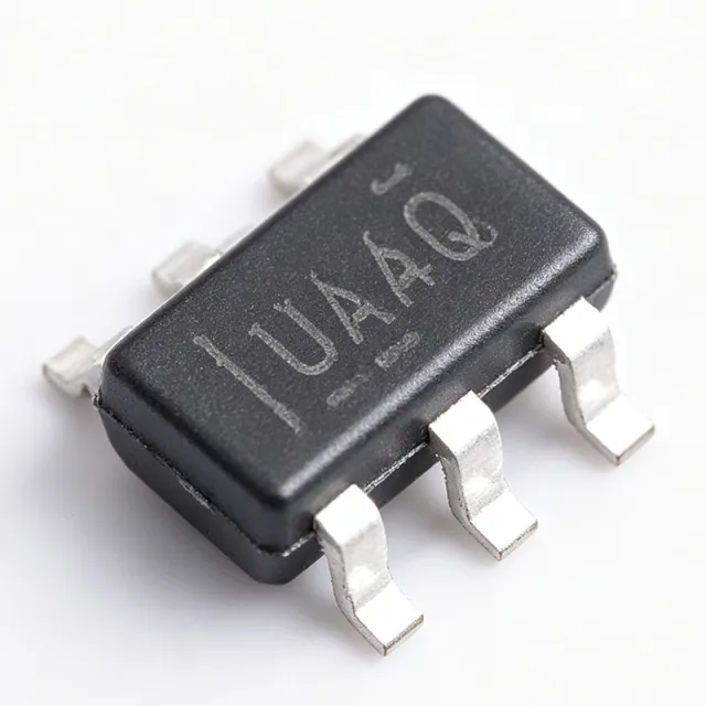
The Texas Instruments TS5A3159QDBVRQ1 is an automotive-qualified (AEC-Q100) single-pole double-throw (SPDT) 2:1 analog switch with 1Ω typical ON-state resistance (1.3Ω max), operating from a 1.65V to 5.5V supply in a 6-pin SOT-23 (DBV) package. An analog switch is a semiconductor device that routes or gates analog and digital signals under the control of a logic-level input. Within the signal-chain hierarchy, the SPDT analog switch sits in the analog switches and multiplexers family, below large multiplexer arrays and alongside transmission-gate logic. An SPDT device connects one common (COM) terminal to either of two throw terminals (NO or NC), making it the fundamental building block of signal routing and redundancy switching. Key features include break-before-make switching, which prevents momentary channel shorting during transition and eliminates signal distortion when a signal source moves between paths; an excellent total harmonic distortion (THD) specification that preserves audio and precision-signal integrity; and low ON-resistance matching and flatness, which minimize signal error across the input range. The device operates from a single 1.65V to 5.5V supply, compatible with 1.8V, 2.5V, 3.3V, and 5V logic systems. The switch core uses a low-charge-injection MOS transmission-gate architecture with approximately 8pF typical ON capacitance (per TI family data), limiting high-frequency insertion loss in data and RF routing paths. The digital IN pin is logic compatible across the full supply range, and the -Q1 suffix denotes AEC-Q100 qualification with -40C to +125C operation for automotive environments. Typical applications include automotive audio source selection, sensor-signal multiplexing in battery-management and body-control modules, UART/SPI/SMBus line sharing, and general-purpose signal gating in industrial systems. The 2.9mm x 1.6mm SOT-23-6 footprint suits densely populated boards. Design tip: terminate or AC-ground unused throw terminals to reduce crosstalk, and place the device close to the signal source to minimize parasitic trace capacitance. This page synthesizes distributor pricing, drop-in alternatives, comparison tables, and practical design notes not found in the manufacturer datasheet.

TS5V330D - 300MHz Quad SPDT Video Switch | Texas Instruments
The Texas Instruments TS5V330D is a four-channel 2:1 SPDT video switch with 300 MHz bandwidth, -63 dB crosstalk, and a 4 V to 5.5 V supply range, housed in a 16-pin SOIC package. Each channel can route one of two video inputs to one output, while a shared enable input controls the switch state. The low on-state resistance makes the device suitable for analog video routing systems requiring high-frequency signal integrity. A video switch is an analog multiplexer or demultiplexer used to route high-speed video signals between sources and destinations. Within the signal-chain hierarchy, this quad SPDT arrangement provides four independently selectable 2:1 paths, combining space-efficient routing with a common control interface. Unlike a digital multiplexer, an analog video switch must preserve signal amplitude, bandwidth, crosstalk performance, and impedance continuity as the selected path changes. Key features include 300 MHz bandwidth, 4 V to 5.5 V operation, low on-state resistance, -63 dB crosstalk, and four channels in one package. The 300 MHz bandwidth supports high-definition and component or progressive video formats, while the 2:1 configuration allows a source-selection function without requiring a separate downstream mux. The shared enable input simplifies system control and supports coordinated switching of all four channels. The TS5V330 operates as a 4-bit, 1-of-2 multiplexer or demultiplexer. Each SPDT path provides a dedicated signal terminal for each input and an output terminal, enabling either video-routing or signal-selection use. A 16-pin SOIC package supports conventional surface-mount assembly, while its operating-temperature range of -40 °C to 85 °C suits industrial and commercial equipment. Exact on-resistance, insertion loss, return loss, channel capacitance, and enable timing values should be taken from the manufacturer datasheet when sizing the complete signal path. Typical uses include video-source selection, video test equipment, broadcast and professional video routing, imaging-system interface switching, and multiple-input display systems. In each case, the 300 MHz bandwidth permits high-frequency analog signals while the four integrated channels reduce the number of separate switch packages required on a board. Designers should preserve controlled-impedance routing and provide a low-impedance return path to avoid reflections and additional crosstalk. A key design consideration is the relationship between source impedance, switch on-state resistance, load capacitance, and allowable video bandwidth. Keep traces short, use impedance-controlled routing where applicable, and place the device close to the signal source. For systems requiring channel-to-channel switching, ensure the enable timing and control levels satisfy the timing budget of the video source. This page consolidates the verified TS5V330D device characteristics, application guidance, comparison fields, and PCB design considerations into one engineering-focused reference. It also separates confirmed manufacturer information from parameters that still require confirmation in the latest device documentation.
TS5V330DR - 300MHz Quad SPDT Video Switch | Texas Instruments (Tape & Reel)
The Texas Instruments TS5V330DR is a four-channel 2:1 SPDT video switch with 300 MHz bandwidth, -63 dB crosstalk, and a 4 V to 5.5 V supply range, housed in a 16-pin SOIC package. Each channel can route one of two video inputs to one output, while a shared enable input controls the switch state. The low on-state resistance makes the device suitable for analog video routing systems requiring high-frequency signal integrity. A video switch is an analog multiplexer or demultiplexer used to route high-speed video signals between sources and destinations. Within the signal-chain hierarchy, this quad SPDT arrangement provides four independently selectable 2:1 paths, combining space-efficient routing with a common control interface. Unlike a digital multiplexer, an analog video switch must preserve signal amplitude, bandwidth, crosstalk performance, and impedance continuity as the selected path changes. Key features include 300 MHz bandwidth, 4 V to 5.5 V operation, low on-state resistance, -63 dB crosstalk, and four channels in one package. The 300 MHz bandwidth supports high-definition and component or progressive video formats, while the 2:1 configuration allows a source-selection function without requiring a separate downstream mux. The shared enable input simplifies system control and supports coordinated switching of all four channels. The TS5V330 operates as a 4-bit, 1-of-2 multiplexer or demultiplexer. Each SPDT path provides a dedicated signal terminal for each input and an output terminal, enabling either video-routing or signal-selection use. A 16-pin SOIC package supports conventional surface-mount assembly, while its operating-temperature range of -40 °C to 85 °C suits industrial and commercial equipment. Exact on-resistance, insertion loss, return loss, channel capacitance, and enable timing values should be taken from the manufacturer datasheet when sizing the complete signal path. Typical uses include video-source selection, video test equipment, broadcast and professional video routing, imaging-system interface switching, and multiple-input display systems. In each case, the 300 MHz bandwidth permits high-frequency analog signals while the four integrated channels reduce the number of separate switch packages required on a board. Designers should preserve controlled-impedance routing and provide a low-impedance return path to avoid reflections and additional crosstalk. A key design consideration is the relationship between source impedance, switch on-state resistance, load capacitance, and allowable video bandwidth. Keep traces short, use impedance-controlled routing where applicable, and place the device close to the signal source. For systems requiring channel-to-channel switching, ensure the enable timing and control levels satisfy the timing budget of the video source. This page consolidates the verified TS5V330DR device characteristics, application guidance, comparison fields, and PCB design considerations into one engineering-focused reference. It also separates confirmed manufacturer information from parameters that still require confirmation in the latest device documentation.

TXB0104D - 4-Bit Bidirectional Level Translator, 100Mbps | TI
The Texas Instruments TXB0104D is a 4-bit bidirectional voltage-level translator with automatic direction sensing, delivering up to 100 Mbps data rates in a 14-pin SOIC (D) package, with VCCA from 1.2V to 3.6V and VCCB from 1.65V to 5.5V plus +/-15 kV ESD protection. A voltage-level translator (also called a level shifter) is a logic IC that interfaces digital circuits operating at different supply voltages, allowing a 1.8V microcontroller to safely communicate with a 3.3V or 5V peripheral. Level translators sit within the broader logic IC family, alongside buffers, transceivers, and bus switches, and are a fundamental part of system power-management and signal-chain design wherever mixed-voltage domains coexist. Key features of the TXB0104D include fully automatic direction sensing that eliminates the direction-control pin required by conventional transceivers, universal translation among 1.2V, 1.5V, 1.8V, 2.5V, 3.3V, and 5V nodes, and a 100 Mbps maximum data rate that supports fast embedded buses. An active-high OE input tri-states all eight I/Os when low, providing board-level power sequencing isolation. Architecturally, the TXB family uses two separate configurable power-supply rails: port A tracks VCCA and port B tracks VCCB. Internal one-shot circuits sense edges and briefly drive stronger pull-up/pull-down transistors, while a 4 kOhm series switch holds the level in static conditions. This push-pull CMOS design requires neither pull-up resistors nor direction control, but it does mean the TXB0104 is suited to push-pull CMOS outputs only, not open-drain buses unless replaced by the TXS family. Typical applications include MCU-to-peripheral interfacing across mixed voltage domains, SPI and UART signal translation, and general-purpose 1.2V-to-5V logic bridging in industrial and consumer systems. The -40C to +85C operating range covers most commercial and industrial environments. Design consideration: keep VCCA lower than or equal to VCCB, and remember the weak static drive (about 4 kOhm) cannot handle heavy loads, long wires, or pull-up resistors below about 50 kOhm. This page synthesizes verified distributor data, drop-in alternative analysis, and practical design notes not found in the manufacturer datasheet alone.
TXB0104RUTR - 4-Bit Bidirectional Level Shifter | Texas Instruments
The Texas Instruments TXB0104RUTR is a 4-bit bidirectional voltage-level translator with automatic direction sensing and ±15-kV ESD protection (Human Body Model), housed in a 12-pin UQFN (RUT) package measuring 1.7 mm x 2.0 mm. It translates signals between a low-voltage A port operating from 1.2 V to 3.6 V and a higher-voltage B port from 1.65 V to 5.5 V (VCCA <= VCCB), supporting data rates up to 100 Mbps. A voltage-level translator, also called a level shifter, is an integrated circuit in the logic-translation family that enables communication between digital devices operating at different supply voltages. In mixed-voltage systems, a 1.8 V or 3.3 V MCU may need to interface with 5 V peripherals; translators convert logic levels bidirectionally while protecting low-voltage silicon. The TXB0104 belongs to the auto-direction-sensing translator family, eliminating direction-control pins and simplifying both PCB design and firmware. Key features include per-channel automatic direction sensing, ±15-kV HBM ESD protection on all pins, tri-state outputs with an output-enable (OE) pin for bus isolation, and an operating temperature range of -40C to +85C. Low quiescent current and the tiny UQFN footprint suit space-constrained portable designs. Architecturally, the TXB0104 uses a one-shot edge accelerator that speeds rising and falling edges, enabling 100 Mbps operation with low static power. The A port tracks VCCA and the B port tracks VCCB. Partial power-down via OE and Ioff-style isolation make it suitable for hot-insertion environments. Typical applications include SPI, UART, and push-pull GPIO level shifting between MCUs, sensors, SIM card and SD card interfaces, and memory peripherals in mobile, industrial, and consumer products. The push-pull driver topology is not recommended for open-drain buses such as I2C or 1-Wire, as confirmed in TI E2E forum threads. Design tip: power VCCA before VCCB, place 0.1 uF bypass capacitors close to both supply pins, and use the OE pin for sequencing. For open-drain buses, consider TXS0104E instead.

TXB0104W-Q1 - 4-Bit Auto-Direction Level Translator | Texas Instruments
The Texas Instruments TXB0104W-Q1 is an automotive-grade 4-bit bidirectional voltage-level translator with automatic direction sensing, rated for data rates up to 100 Mbps and protected by +/-15 kV IEC ESD protection on the I/O pins, housed in a 12-pin UQFN (RUT) package. Qualified per AEC-Q100 for automotive applications, the W variant supports a VCCA supply range of 1.1 V to 3.6 V and a VCCB range up to 3.6 V, translating between logic families such as 1.2 V, 1.8 V, 2.5 V, and 3.3 V rails. A voltage-level translator is a member of the logic IC family (voltage-level translator -> logic IC -> integrated circuit) that allows two circuit domains operating at different supply voltages to exchange digital signals safely. On mixed-voltage PCBs - for example, a 1.8 V microcontroller talking to a 3.3 V sensor - the translator isolates the rails while preserving logic polarity and timing, preventing overvoltage damage and logic-level misreads. Key features of the TXB0104W-Q1 include automatic direction sensing that eliminates DIR control pins, push-pull topology optimization delivering 100 Mbps throughput, and a compact 12-pin UQFN footprint of approximately 2 mm x 2 mm that saves board area. The +/-15 kV ESD rating (IEC) on the I/O ports adds robustness in harsh automotive electrical environments. According to TI product data, the device uses two separate configurable power-supply rails; the A port tracks VCCA and the B port tracks VCCB. Architecturally, the TXB family uses a two-transistor output driver with an integrated one-shot edge-rate accelerator on each side, giving fast transition times for push-pull CMOS signals. This makes it well suited to SPI, UART, and general-purpose push-pull GPIO translation. Note that, as TI applications guidance states, the TXB architecture is not recommended for open-drain buses such as I2C or 1-Wire, where the internal drivers contend with external pull-ups. Typical applications include automotive body electronics and gateways translating between 1.8 V SoC GPIO and 3.3 V peripherals, infotainment and display module signal interfaces, and industrial control modules requiring AEC-Q100 qualified components. Design tip: keep VCCA ramps before or after VCCB within datasheet sequencing guidance, and place the two 0.1 uF decoupling capacitors directly at the VCCA and VCCB pins; the auto-direction sensing requires push-pull sources on both sides to function reliably. This page synthesizes distributor pricing tiers, verified drop-in alternatives from TI cross-reference discussions, and practical design notes not found in the manufacturer datasheet.
TXB0104YZTR - 4-Bit Auto-Direction Level Translator | TI
The Texas Instruments TXB0104YZTR is a 4-bit bidirectional voltage-level translator with automatic direction sensing, supporting 1.2V to 3.6V on the A port and 1.65V to 5.5V on the B port at data rates up to 100 Mbps, housed in a 12-ball DSBGA (YZT) package measuring 1.9 mm x 1.4 mm with +/-15 kV ESD protection. A voltage-level translator is a logic-interface device that allows integrated circuits operating at different supply voltages - for example a 1.8V microcontroller and a 5V sensor - to exchange digital signals reliably. Within the power-management and interface hierarchy, level translators sit between logic families such as CMOS and TTL, complementing buffers, bus switches, and transceivers in the broader signal-chain category. Without translation, low-voltage logic can be damaged by higher-voltage inputs or fail to meet higher-voltage logic thresholds. Key features of the TXB0104 include its two separate configurable power-supply rails (VCCA tracks the A port, VCCB tracks the B port, with VCCA <= VCCB), auto-direction sensing that eliminates direction-control pins, a maximum propagation delay of 13.7 ns, and 4 kV (HBM) class robustness supplemented by +/-15 kV IEC ESD protection on the I/O lines. The TXB architecture uses a mixed-charge pump output driver that pushes data in either direction without OE-based handshaking. Technically, the device derives its drive from a 4 kOhm output stage optimized for lightly loaded, point-to-point CMOS links; it is not a bus-holder for heavily capacitive or high-fanout loads. The 0.5 mm ball pitch and wafer-scale DSBGA packaging minimize board area, making it attractive for dense portable designs. The output enable (OE) pin tri-states all channels for power-aware sequencing. Typical applications include translating I2C-adjacent push-pull buses, SPI and UART links between 1.8V MCUs and 3.3V or 5V peripherals, SD-card interfaces, and general-purpose GPIO bridging in industrial and consumer systems. A key design consideration: avoid capacitive loads above roughly 30 pF and pull-up/pull-down resistors below about 25 kOhm, because the auto-direction scheme relies on one side driving the line; contested drivers cause bus contention. This page synthesizes distributor pricing, verified specifications, and practical design guidance for the TXB0104YZTR beyond what any single datasheet page provides.

TXB0108PWR - 8-Bit Bidirectional Level Shifter 100Mbps | TI
The Texas Instruments TXB0108PWR is an 8-bit bidirectional voltage-level translator with auto-direction sensing and +/-15-kV ESD protection, housed in a 20-pin TSSOP (PW) package. It translates signals between a 1.2V to 3.6V A port and a 1.65V to 5.5V B port (VCCA <= VCCB), with data rates up to 100 Mbps, making it ideal for mixed-voltage digital systems. A voltage-level translator is a logic IC that enables communication between devices operating at different supply voltages, such as a 1.8V microcontroller and a 3.3V or 5V peripheral. It sits in the hierarchy of logic ICs under level shifters (translators), which are essential in multi-voltage digital systems alongside buffers and bus transceivers. The TXB0108PWR uses auto-direction sensing, eliminating the need for a direction control pin and reducing firmware complexity. Key features include auto-direction sensing, +/-15-kV ESD protection (HBM), a 100 Mbps maximum data rate, and a VCC isolation feature: if either VCC input is at GND, all outputs enter the high-impedance state, enabling partial-power-down operation with Ioff support. The device operates from -40C to +85C. Technically, the TXB0108 uses a one-shot architecture that accelerates low-to-high transitions to achieve 100 Mbps. It is designed for push-pull (totem-pole) CMOS drivers only; for open-drain buses such as I2C, TI recommends the TXS0108E. Output drive is intentionally weak (internal 4 kOhm series resistors), so heavy capacitive loads above ~70 pF reduce achievable speed. Typical applications include 1.8V-to-3.3V microcontroller-to-sensor interfaces, SD card level shifting, UART/SPI signal translation, and FPGA configuration buses. The 100 Mbps capability suits high-speed SPI and UART links. Design tip: ensure VCCA <= VCCB, drive all eight channels push-pull, and place 0.1uF decoupling capacitors close to both VCCA and VCCB pins with short traces for signal integrity.

TXB0108QPWRQ1 - 8-Bit Auto-Direction Level Translator | TI
The Texas Instruments TXB0108QPWRQ1 is an automotive-qualified (AEC-Q100) 8-bit bidirectional voltage-level translator with auto-direction sensing and ±15kV ESD protection, packaged in a 20-pin TSSOP (PW). Port A supports 1.2V to 3.6V supplies while Port B supports 1.65V to 5.5V, enabling translation between any two logic rails in these ranges. A voltage-level translator (also called a logic level shifter) is an interface IC that enables digital devices operating on different supply rails - such as a 1.8V microcontroller and a 5V peripheral - to communicate reliably. Translators sit within the broader logic IC family, under interface and signal-conversion devices, and are essential wherever mixed-voltage systems coexist on one board. Key features include auto-direction sensing that eliminates the need for a direction-control pin, an output-enable (OE) input that places all I/O in Hi-Z when low, and ±15kV IEC ESD protection on I/O pins. The TXB0108-Q1 uses TI TXB-type push-pull architecture, delivering symmetric drive on both ports without external pull-up or pull-down resistors, and supports data rates up to 100 Mbps for 1.2V to 3.6V translation per the datasheet. The device operates from -40C to +125C (AEC-Q100 Grade 1), making it suitable for harsh automotive environments. Its TSSOP-20 package is standard, easy to assemble, and compatible with the commercial TXB0108PWR footprint for design reuse. Typical applications include automotive infotainment and cluster modules interfacing 3.3V MCUs with 5V sensors, mixed-voltage SPI/I2C-style GPIO expansion, industrial control modules, and portable mixed-signal systems bridging 1.8V and 5V rails. Design note: the TXB architecture has relatively weak output drive (not intended for bus-holding or heavy loads); avoid using it for I2C open-drain buses - the TXS family is a better fit. Pull OE low during power sequencing to prevent bus contention.
TXG4021-Q1 - ±40V 2-bit Ground-Level Translator | TI
The Texas Instruments TXG4021-Q1 is an automotive-grade, 2-bit, fixed-direction, non-galvanic ground-level translator supporting logic-level shifting between 1.71V and 5.5V and ground-level shifting up to ±40V, delivered in an 8-pin SOIC (D) package with a maximum data rate of 264 Mbps. A ground-level translator is a specialized type of voltage level shifter within the broader logic IC family. While standard level translators only shift logic thresholds between supply domains (for example 3.3V to 5V), a ground-level translator also bridges systems whose ground references differ by tens of volts - a common condition in automotive and industrial environments where load currents in shared returns lift local ground potentials. The TXG402x-Q1 family solves this without galvanic isolation, offering a lower-cost, smaller-footprint alternative to digital isolators where only ground-offset tolerance is needed. Key features include the ±40V ground-shift tolerance, the 1.71V to 5.5V logic-level range on both sides, a fixed (unidirectional) direction configuration with two channels in a 1/1 arrangement, and a 264 Mbps maximum data rate. The -Q1 variant is qualified for automotive applications per TI's automotive qualification flow, supporting AEC-oriented design flows. Architecturally, the device is non-galvanic: input and output stages share a common substrate reference topology that tolerates large ground differentials while translating logic swings, unlike optocoupler or transformer-based isolators. This yields lower propagation delay and lower cost than isolation approaches, with the trade-off that the ground offset is tolerated rather than fully isolated. Typical applications include automotive body electronics and lighting modules, motor-drive gate-drive interfaces where ground lift occurs, and industrial PLC I/O cards bridging a 1.71V-5.5V controller domain to a high-side domain with a shifted ground. Design consideration: because the part is unidirectional, confirm signal direction is fixed in your topology; it cannot be used for bidirectional buses such as I2C without external direction handling. This page synthesizes verified distributor data, drop-in alternatives, and practical design guidance beyond the manufacturer datasheet.