Power Management
ژێرپۆلەکان
بەرهەمەکان (2,800+)

TPS92513HVDGQR - 65V 1.5A Buck LED Driver HVSSOP-10 | TI
The Texas Instruments TPS92513HVDGQR is a 65-V, 1.5-A step-down (buck) LED driver with an integrated N-channel MOSFET, housed in a 10-pin HVSSOP (DGQ) PowerPAD package. It uses analog current adjustment via an external sense resistor and supports both analog and PWM dimming for high-current LED strings. The wide 4.5 V to 65 V input range allows direct connection to 12 V and 24 V nominal buses as well as industrial 48 V rails, while the integrated 200 mOhm MOSFET simplifies the BOM and enables high step-down ratios in compact PCB areas. A buck LED driver is a switch-mode DC-DC converter that regulates the current through an LED string rather than the voltage across it, which provides uniform brightness regardless of forward-voltage variation between LEDs. Within the broader power-management IC (PMIC) hierarchy, the TPS92513HV sits in the LED-driver category, which is itself a subset of switching regulators alongside buck, boost, and buck-boost converters optimized for light-load efficiency. Key features include cycle-by-cycle overcurrent protection, thermal shutdown, an enable/shutdown pin, an analog adjust (ADJ) input for current programming, and a PWM dim input. The peak-current-mode control topology yields good line and load regulation and supports user-selectable switching frequencies via an external resistor. The HVSSOP-10 PowerPAD package exposes the die ground pad for low thermal resistance (about 45 C/W on a standard 2 oz. 4-layer board), which keeps junction temperatures in check at full 1.5 A output. Designers can also synchronize the device to an external clock for EMI-sensitive applications. Typical applications include architectural and commercial LED lighting, automotive interior and exterior LED drivers, industrial signage, emergency lighting, and 24 V track-lighting fixtures. The 65-V rating gives substantial transient headroom on 24 V industrial buses where load-dump-style surges are common. The wide VIN range also supports daisy-chained LED luminaires powered from a single high-voltage rail. When laying out the PCB, place the input ceramic bypass, the bootstrap capacitor, and the freewheeling Schottky diode as close to the IC as possible to minimize parasitic loop inductance. The exposed pad must be soldered to a copper pour spanning multiple thermal vias to keep junction temperatures within the 150 C thermal-shutdown limit during continuous 1.5 A operation.

TPS92515HVQDGQRQ1 - 65V 2A Buck LED Driver, AEC-Q100 | Texas Instruments
The Texas Instruments TPS92515HVQDGQRQ1 is a 65-V automotive 2-A shunt-PWM dimmable LED driver integrating an N-channel MOSFET, high-side current sense, and shunt PWM dimming circuitry, housed in a thermally-enhanced 10-pin HVSSOP (DGQ) PowerPAD package. It is designed for high-brightness LED lighting applications where efficiency, high bandwidth, PWM and/or analog dimming, and small PCB area are important. An LED driver is a power-management integrated circuit that regulates current through one or more LED strings to maintain consistent luminance regardless of input voltage, LED forward-voltage variation, or temperature. LED drivers sit hierarchically between DC-DC converters (broader switching-power category) and discrete linear current regulators; the buck (step-down) topology used in the TPS92515HV-Q1 family is the most common for high-current, moderate-to-high input-voltage strings because it delivers high efficiency (typically >90 percent) without the heat dissipation of linear regulators. Key features include a 4.5-V to 65-V operational input range, integrated 200-mOhm N-channel FET, constant-off-time peak-current control, analog and shunt-PWM dimming capability, and AEC-Q100 Grade 1 qualification (operating from -40C to +125C). The HVSSOP-10 PowerPAD package exposes a thermal pad that lowers junction-to-ambient resistance (theta_JA approximately 50 C/W on a 4-layer JEDEC board), enabling 2-A continuous LED current without an external heatsink in properly laid-out designs. The high-side current-sense scheme eliminates the need for a ground-side shunt and avoids ground-loop noise coupling in long LED-cable harnesses. The device uses constant-off-time peak-current control with a simple external RC network to program switching frequency, and the integrated FET removes a major source of layout-dependent ringing and EMI. Current calibration trims the nominal LED current at a single reference point, reducing string-to-string brightness mismatch that would otherwise require hand-binning. Typical applications include automotive headlamps, daytime running lights, rear combination lamps, and turn signals, plus industrial high-bay lighting and architectural fixtures operating from 12-V or 24-V buses. Industrial LED signage, machine-vision illumination, and emergency-vehicle light bars are additional high-volume use cases. When VIN is above the LED string forward voltage by only a few volts, the driver remains efficient; when VIN is significantly higher, the duty cycle shrinks and switching losses dominate, so thermal layout becomes critical.
TPS92515QDGQRQ1 - 42V 2A Automotive LED Driver | Texas Instruments
The Texas Instruments TPS92515QDGQRQ1 is a 42-V, 2-A automotive-grade buck LED driver with an integrated N-channel MOSFET, high-side current sense, and shunt FET PWM dimming capability, packaged in a 10-pin HVSSOP (DGQ) with PowerPAD. It is qualified to AEC-Q100 Grade 1 and supports analog plus PWM dimming for precise brightness control in headlamp, daytime running light, and interior lighting systems. What is a buck LED driver? A buck (step-down) LED driver is a switching DC-DC converter that regulates current through a string of LEDs by chopping the input voltage down to the LED forward voltage plus headroom. Buck LED drivers sit inside the broader hierarchy: LED driver -> lighting IC -> power management IC -> semiconductor. Compared with linear LED drivers they achieve much higher efficiency at large VIN-VOUT deltas, which is critical for automotive 12-V/24-V battery rails. Key features include a 42-V absolute maximum input (4.5-V to 42-V operating range), 2-A continuous switch current, integrated 250-mOhm N-channel FET, high-side current sensing for ground-referenced LED cathodes, 100:1 analog dimming range, and 1000:1 PWM dimming range via an external shunt FET. Cycle-by-cycle current limit and thermal shutdown provide fault protection. According to TI's product page, the HVSSOP-10 PowerPAD delivers a junction-to-ambient thermal resistance of approximately 47 C/W on a standard JEDEC 4-layer board. The TPS92515QDGQRQ1 uses peak-current-mode control with internal slope compensation to maintain stability across the full duty-cycle range. The high-side sense scheme eliminates the need for a ground-side shunt, simplifying PCB routing and improving efficiency by 2-5% versus low-side sense designs. The shunt-FET PWM dimming input permits >1 kHz dimming frequencies without audible noise. Typical applications include automotive LED headlights, fog lamps, daytime running lights, rear combination lamps, and architectural or industrial lighting that requires AEC-Q100 reliability. The wide VIN range also supports industrial 24-V nominal bus systems. When designing with this device, allocate at least 1 square cm of copper pour under the PowerPAD and use low-ESR ceramic input capacitors to handle the buck-switching ripple. Verify that the LED string forward voltage leaves sufficient headroom (typically >1.5 V) for current-sense accuracy at minimum VIN. This page synthesizes distributor pricing, AEC-Q100 cross-references, and drop-in alternatives compiled from TI's part details page and authorized distributor listings - context you will not find in the standalone datasheet.

TPS92630QPWPRQ1 - 3-Ch 150mA Linear LED Driver, AEC-Q100 | TI
The Texas Instruments TPS92630QPWPRQ1 is an automotive-grade, three-channel linear LED driver with analog and PWM dimming, delivering up to 150 mA per channel in a 16-pin HTSSOP (PWP) package with PowerPAD exposed pad. It operates across 9 V to 18 V nominal supply (with transient tolerance to 40 V) and integrates full diagnostics and protection features, including open-LED, short-to-GND, short-to-VBAT, and thermal shutdown. What is a linear LED driver? A linear LED driver is a constant-current regulator that places the LED string in series with a pass transistor whose conduction is modulated to maintain a programmed current. Unlike switching drivers, linear regulators introduce no EMI and no switching ripple, which makes them ideal for noise-sensitive analog lighting and for meeting CISPR 25 EMI limits in automotive modules. The TPS92630-Q1 belongs to the broader power management IC family (LED driver -> constant-current driver -> lighting driver -> PMIC) and is optimized for medium-power automotive lighting subsystems. Key features include a 150 mA per-channel current set by a single external sense resistor, 1000:1 analog dimming range, 1000:1 PWM dimming at 200 Hz, individual channel enable/diagnostic pins, and a fault output (FAULT) that asserts on any protection event. The HTSSOP-16 PowerPAD package achieves a theta_JA near 38 C/W on a 4-layer JEDEC JESD51 board, enabling compact PCB layouts without an external heatsink at typical 60-100 mA operating currents. The TPS92630-Q1 uses three independent linear current sinks, each with its own diagnostic comparator and PWM latch. A shared reference and bias block minimize channel-to-channel mismatch. Internal slope compensation on the analog dimming input ensures monotonic response across the 1000:1 range and prevents current crowding in multi-string arrays. Typical applications include automotive rear combination lamps, daytime running lights, interior ambient lighting, and ADAS indicator LEDs. The wide 4.5 V to 40 V transient tolerance also makes it robust against load-dump events on 12 V automotive buses. When designing with this part, place the 1 uF VIN bypass capacitor close to the IC and route the PowerPAD copper pour to a low-impedance ground plane. Verify thermal performance under worst-case VIN and full-current operation, and use the FAULT pin for system-level diagnostics in compliance with ISO 26262 functional-safety requirements. This page synthesizes distributor pricing, drop-in alternatives, and practical design notes not found in the manufacturer datasheet.

TPS92691 - Multi-Topology LED Driver | Texas Instruments
The Texas Instruments TPS92691 is a versatile multi-topology LED driver controller designed for step-up (boost), step-down (buck), SEPIC, and flyback topologies. It integrates a rail-to-rail current sense amplifier, enabling accurate LED current regulation across a wide range of applications. The device operates with a fixed-frequency peak current mode control scheme, with programmable switching frequency, slope compensation, and soft-start timing. It supports both analog and PWM dimming, making it suitable for automotive, industrial, and general lighting systems. An LED driver is a power management IC that regulates the current flowing through one or more LEDs, ensuring consistent brightness and protecting the LEDs from current surges. The TPS92691 belongs to the family of switching LED drivers, which use inductive or capacitive energy storage to efficiently convert input voltage to the required LED current. This controller sits between the power source and the LED string, providing closed-loop regulation and dimming capabilities. Key features of the TPS92691 include a wide input voltage range, programmable switching frequency up to 1 MHz, and a rail-to-rail current sense amplifier that allows low-side or high-side sensing. The device also features an internal 10-µA soft-start current source, an external soft-start capacitor for controlled startup, and a COMP pin that is clamped to the SS pin until LED current nears regulation. These features enable smooth startup and stable operation across varying load conditions. The TPS92691 is available in a 16-pin HTSSOP (PWP) package, which provides a compact footprint with exposed thermal pad for improved heat dissipation. The device is designed for high-efficiency operation, with typical efficiencies above 90% in boost and buck configurations. It also includes protection features such as thermal shutdown and overcurrent protection, enhancing system reliability. Typical applications include automotive LED headlights, daytime running lights, industrial LED lighting, and backlighting for displays. The device's flexibility in topology and dimming methods makes it a preferred choice for designers seeking a single controller for multiple LED driver designs. When designing with the TPS92691, it is important to select appropriate external components such as the inductor, MOSFET, and sense resistor to meet the desired output current and efficiency. Proper PCB layout, including minimizing parasitic inductance and ensuring adequate thermal management, is critical for optimal performance.
TPS92691-Q1 - 65V AEC-Q100 LED Driver Controller | TI
The Texas Instruments TPS92691-Q1 (TPS92691QPWPTQ1) is an automotive-qualified multi-topology LED driver controller supporting boost, buck, buck-boost, SEPIC, Cuk, and flyback topologies. It operates from a wide 4.5 V to 65 V input and integrates a 65-V rail-to-rail current sense amplifier with better than ±3% LED current accuracy over a junction temperature range of +25°C to +140°C and a 0 V to 60 V output common-mode range, enabling both high-side and low-side current sensing. The device is supplied in a 16-pin HTSSOP (PWP) package. An LED driver controller is a power management IC that regulates current through LED strings using a switching regulator architecture. Within the power management IC hierarchy, it sits between generic DC-DC controllers and dedicated constant-current LED drivers, adding dimming control, fault protection, and LED-specific features. Peak current mode control is a control technique in which the switch current is sensed and compared against an error-amplifier-derived threshold on a cycle-by-cycle basis, giving inherent cycle limiting and simple loop compensation. Key features include fixed-frequency peak current mode control with programmable switching frequency, programmable slope compensation for stable operation at duty cycles above 50%, programmable soft-start timing to limit inrush current, and a dedicated PWM dimming input that linearly varies LED brightness by modulating the duty cycle of the voltage applied to the PWM pin. Analog dimming is also supported, allowing flexible brightness control in automotive lighting systems. Architecturally, the integrated high-voltage current sense amplifier is the differentiating block: by tolerating a 60 V common-mode input, it removes the need for a dedicated low-side sense resistor path in high-rail strings and simplifies short-circuit diagnostics. The controller generates gate drive for an external MOSFET, so output power is set by external components rather than IC limits. Typical applications include automotive headlights, daytime running lights (DRL), fog lamps, LED backlighting, and industrial lighting driven from 12 V, 24 V, or 48 V automotive and industrial buses. Design consideration: choose the switching frequency and slope compensation together - higher frequency shrinks the inductor but increases switching loss; slope compensation must be set based on the sensed inductor current downslope to avoid subharmonic oscillation at duty cycles above 50%.

TPS92692QPWPRQ1 - AEC-Q100 Boost/Step-Down LED Controller | TI
The Texas Instruments TPS92692QPWPRQ1 is a high-accuracy, peak-current-mode LED controller designed to support step-up (boost) and step-down (buck) LED driver topologies in automotive lighting applications. Housed in a 20-pin HTSSOP (PWP) package with PowerPAD exposed thermal pad, the device integrates a rail-to-rail current sense amplifier, an internal PWM dimming generator, and spread-spectrum frequency modulation for improved EMI compliance. According to the TI datasheet, the switching frequency is programmable from 80 kHz to 800 kHz and the output voltage range extends from 3 V to 65 V, enabling both low-voltage battery-fed and high-voltage multi-LED-string architectures. A peak-current-mode LED controller is a power-supply control IC that regulates inductor current on a cycle-by-cycle basis to maintain a precisely measured LED load current. This controller class sits within the broader hierarchy of DC-DC switching controllers -> LED drivers -> power management ICs -> automotive-qualified analog semiconductors. Peak-current-mode control offers inherent cycle-by-cycle overcurrent protection and simplified loop compensation compared to voltage-mode control, making it well suited to the variable LED loads seen in adaptive driving beam and matrix-LED headlamp systems. Key features of the TPS92692QPWPRQ1 include analog and PWM dimming capability, high-side current sensing up to ±700 mV full-scale, an internal PWM generator that allows dimming without an external MCU, and spread-spectrum frequency modulation that reduces peak EMI emissions to ease CISPR 25 Class 5 compliance. The device supports both boost (step-up) and buck (step-down) operation from the same controller, allowing a single BOM to cover high-beam, low-beam, daytime running lights, and rear-lighting topologies. The HTSSOP-20 PowerPad package reduces theta_JA and supports sustained operation at high switching currents in space-constrained underhood environments. Architecturally, the device combines a precision transconductance error amplifier, a high-side current sense input (HI-SNS/LO-SNS), a programmable oscillator with spread-spectrum dithering, a PWM dimming latch, and a gate driver capable of driving external MOSFETs. This partitioning enables a designer to size the inductor, MOSFETs, and sense resistor for the specific string voltage and current without controller-side limitations. The internal soft-start and fault timer (with thermal shutdown, LED open/short detection, and fault output) simplify ASIL-relevant safety analysis for OEM headlamp modules. Typical applications include automotive front lighting (high beam, low beam, DRL), matrix-LED adaptive driving beam modules, rear lighting (tail, brake, turn), and high-current industrial LED strings. The AEC-Q100 Grade 1 rating makes it suitable for underhood operation across -40 °C to +125 °C ambient. When designing with this device, pay attention to PCB layout of the current-sense traces (Kelvin connection required to the sense resistor) and to thermal management of the PowerPAD - sustained boost operation at high duty cycle can dissipate several watts.
TPSM13604H - 4A Step-Down Power Module | Texas Instruments
The Texas Instruments TPSM13604H is a SIMPLE SWITCHER power module that integrates a step-down DC-DC converter with an inductor and other passive components into a compact 7-TO-PMOD package. It accepts an input voltage from 5V to 36V and delivers an adjustable output voltage from 3V to 16V with up to 4A of continuous output current. The module is designed for easy implementation, requiring only three external resistors and four external capacitors to complete the power solution. A power module is a complete DC-DC converter solution that integrates the controller, power FETs, inductor, and often compensation circuitry into a single package. This integration simplifies PCB layout, reduces design time, and improves thermal performance compared to discrete solutions. The TPSM13604H belongs to the SIMPLE SWITCHER family, which is known for its ease of use and robust performance in industrial, automotive, and communications applications. Key features include a wide input voltage range of 5V to 36V, adjustable output voltage down to 3V, and a maximum output current of 4A. The module offers exceptional power conversion efficiency, line and load regulation, and output accuracy. It includes protection features such as thermal shutdown, input undervoltage lockout, output over-voltage protection, short-circuit protection, and output current limit. Additionally, it supports start-up into a pre-biased output and allows the switching frequency to be adjusted up to 700 kHz with a single resistor. The TPSM13604H uses an innovative package that enhances thermal performance and allows for hand or machine soldering. The 7-TO-PMOD package is designed for surface-mount assembly and provides excellent heat dissipation. The module operates over a junction temperature range of -40°C to +125°C, making it suitable for harsh environments. Typical applications include point-of-load (PoL) converters for FPGAs, ASICs, and microprocessors, as well as industrial control systems, test and measurement equipment, and automotive infotainment systems. The wide input range and high output current make it ideal for systems powered from 12V or 24V rails. When designing with the TPSM13604H, ensure proper input and output capacitance to maintain stability and minimize ripple. The adjustable output voltage is set by an external resistor divider, and the switching frequency can be programmed with a single resistor. Adequate thermal management is essential when operating at high output currents and high input-to-output voltage differentials.
TPSM265R1SILR - 65V Input 100mA Buck Power Module | Texas Instruments
The Texas Instruments TPSM265R1SILR is a 3V to 65V input, 100mA step-down DC-DC power module with an adjustable output voltage range of 1.233V to 15V, housed in a compact 2.8 mm x 3.7 mm uSIP module package. It integrates a synchronous buck controller, power MOSFETs, and the output inductor into a single easy-to-use device. A step-down power module is a complete DC-DC converter solution in one package. Unlike a discrete buck regulator design, a power module places the controller, switching FETs, inductor, and passives inside a single molded package, eliminating magnetics selection and layout optimization from the design cycle. Power modules sit at the top of the point-of-load (PoL) power hierarchy: voltage regulator -> switching regulator -> buck converter -> integrated power module, all within the broader power management IC (PMIC) category. Key differentiating features of the TPSM265R1SILR include an ultra-low quiescent current of 10.5 uA, which enables very high light-load efficiency in always-on and battery-backup systems; a maximum continuous input voltage of 65 V, providing robust headroom for industrial 24 V and 48 V nominal buses; and full integration of the power stage and inductor for a minimal external component count. Fixed 3.3 V and 5 V output options are also available in the same family. Technically, the module employs a synchronous step-down topology with integrated high-side and low-side MOSFETs and an internal output inductor. The wide 3V to 65V input range with an internal controller and protection features allows direct connection to industrial and automotive-style supply rails, reducing the need for a front-end transient suppressor stage in moderately protected systems. Ultra-low IQ supports low standby power in always-connected nodes. Typical applications include industrial programmable logic controller (PLC) I/O and sensor supply rails, 24V/48V auxiliary bias supplies for field transmitters and gate drivers, and building-automation or battery-powered monitoring nodes where 10.5 uA quiescent current extends battery life. The small 2.8 mm x 3.7 mm footprint also suits dense multi-rail boards. Design consideration: because the inductor is internal, verify the estimated thermal and output-current requirements stay within the 100 mA rating across your input voltage and ambient temperature range, and follow the TI datasheet layout guidelines for input capacitance placement. This page synthesizes distributor pricing, drop-in family alternatives, and practical design notes not found in the manufacturer datasheet.

TPSM33615FRDNR - 36V 1.5A Sync Buck Module | Texas Instruments
The Texas Instruments TPSM33615FRDNR is a 3-V to 36-V input, 1-V to 15-V output, 1.5-A synchronous buck power module integrated in a HotRod QFN-FCMOD (RDN) package with 11 pins. Headline parameters include 36-V maximum input voltage, 1.5-A continuous load current, and 88% typical efficiency, all delivered in a 3.5 mm x 4.5 mm surface-mount footprint. A buck converter (step-down switching regulator) is a switching-converter topology that reduces a higher DC input voltage to a lower regulated DC output voltage using an inductor, capacitor, and synchronous MOSFET switches. It sits within the broader power management IC hierarchy: buck converter -> DC-DC converter -> switching regulator -> power management IC. A power module such as the TPSM33615FRDNR integrates the controller, MOSFETs, inductor, and compensation network into one package, simplifying PCB layout and reducing design risk versus discrete buck implementations. Key features include 1.5-uA quiescent current, 1-MHz fixed switching frequency, programmable output voltage from 1 V to 15 V, and selectable PFM or FPWM light-load operation. The HotRod QFN-FCMOD package reduces parasitic inductance and improves thermal performance. Integrated protections include over-current, over-temperature, under-voltage lockout, automatic fault recovery, and 1% output voltage accuracy across load and line. The integrated inductor and shielding minimize radiated EMI, which is critical for industrial and instrumentation applications that must pass CISPR 25 or CISPR 32. Technically, the TPSM33615FRDNR uses a peak current-mode control topology with internal compensation, an external RT resistor to program switching frequency, and a MODE pin to select PFM (light-load efficiency) versus FPWM (constant-frequency low-noise) behavior. The HotRod flip-chip QFN package eliminates bond wires, reducing switching-node ringing and DC resistance losses. Typical applications include industrial 24-V rail point-of-load regulation, factory automation sensors, building automation controllers, low-noise bias supplies for analog front ends, and portable or battery-powered equipment operating from multi-cell lithium packs. The wide 3-V to 36-V input range supports 12-V and 24-V industrial buses directly. When designing with this device, keep the input capacitors close to VIN and PGND pins to minimize switching-node ringing, and connect the exposed thermal pad to a sufficient ground copper pour. Select PFM mode for highest light-load efficiency, or FPWM when low EMI is the top priority. This page synthesizes distributor pricing, drop-in alternatives, design notes, and application guidance not found in the manufacturer datasheet alone, giving engineers a single reference for component selection, PCB implementation, and sourcing decisions.
TPSM53604RDAR - 36V 4A Step-Down Power Module | TI
The Texas Instruments TPSM53604RDAR is a 36-V input, 4-A step-down DC/DC power module that integrates power MOSFETs, a shielded inductor, and passives in a thermally enhanced 15-pin Enhanced HotRod QFN package measuring 5.5 mm x 5 mm x 4 mm, delivering an adjustable 1 V to 7 V output from a 3.8 V to 36 V input. A power module is a highly integrated point-of-load (PoL) DC/DC converter: within the broader hierarchy of power management ICs, a step-down (buck) converter reduces a higher input voltage to a lower regulated output, and a power module goes one step further by co-packaging the controller or converter IC, switching MOSFETs, inductor, and key passives into a single surface-mount package. This integration eliminates inductor selection and magnetics design from the engineering workflow, dramatically reducing board area, bill-of-materials count, and design risk compared with a discrete buck converter solution. Key features of the TPSM53604 include its wide 3.8 V to 36 V input range, which directly supports 12-V, 24-V, and industrial 24 V nominal rails with transient headroom; an adjustable output spanning 1 V to 7 V; a continuous 4-A output current rating; and a fixed-frequency peak-current-mode control topology with optimized internal compensation. The Enhanced HotRod QFN construction places the die close to the package pins, minimizing parasitic inductance for low EMI and improved thermal performance. Technically, the module integrates a shielded inductor that produces low radiated electromagnetic emissions, simplifying CISPR-class EMI compliance work. The thermally enhanced package dissipates heat through the PCB, and the simple footprint with all pins on the perimeter makes layout and inspection straightforward. Shutdown quiescent operation and enable functionality support low standby power designs. Typical applications include industrial automation and PLC I/O modules, 12-V and 24-V distributed power systems, test and measurement instrumentation, telecom and networking equipment auxiliary rails, and embedded processor point-of-load supplies derived from wide-input industrial buses. Design consideration: at high input voltages and high output current, verify junction temperature using the datasheet thermal derating curves; adequate PCB copper area beneath the module is the primary thermal solution. This page synthesizes verified distributor data, same-family drop-in alternatives, and practical design guidance not found in the manufacturer datasheet alone. Pricing shown reflects distributor data as of 2026-10-19.
TPSM5601R5 - 60V In, 1.5A Step-Down Power Module | TI
The Texas Instruments TPSM5601R5 is a highly integrated 1.5-A step-down DC/DC power module combining a 60-V maximum input converter, power MOSFETs, a shielded inductor, and support passives in a thermally enhanced 5-mm x 5.5-mm x 4-mm 15-pin Enhanced HotRod QFN package. It delivers an adjustable output voltage of 1.0 V to 6 V from a 4.2-V to 60-V input range with a fixed 400-kHz switching frequency. A power module is a complete DC-DC converter solution that integrates the controller, switching MOSFETs, inductor, and compensation network into a single surface-mount package. Within the power management hierarchy (power module -> step-down converter -> DC-DC converter -> power management IC), modules eliminate magnetics selection and loop compensation design, reducing time-to-market and layout risk compared to discrete converter solutions. Key features include the wide 60-V input rating suited to 24-V and 48-V industrial rails with transient headroom, an output range of 1.0 V to 6 V set by a single external resistor divider, and as few as four external components for the complete solution. The Enhanced HotRod QFN construction places the die directly against the thermal pad, delivering low EMI, excellent thermal performance, and all pins accessible from the package perimeter for simple layout and inspection. The internal compensation and integrated shielded inductor provide stable operation across the load range while reducing solution height and BOM count. The device operates from a -40C to +125C junction temperature range, supporting industrial and automotive-adjacent environments. The TPSM5601R5S variant adds spread-spectrum operation for lower EMI peaks, and the TPSM5601R5H variant extends output capability up to 16 V. Typical applications include 24-V and 48-V industrial bus power supplies, factory automation and PLC I/O modules, test and measurement point-of-load rails, and distributed power systems that need a compact, regulated 1-V to 6-V rail from a wide input. Design tip: because the inductor is integrated, thermal design centers on the PCB copper pour under the thermal pad - provide at least a 1-square-inch ground plane with thermal vias for reliable operation at full 1.5-A load at elevated ambient temperatures.
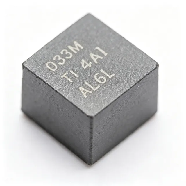
TPSM81033VCDR - 2A 2.4MHz Synchronous Boost Module | TI
The Texas Instruments TPSM81033VCDR is a 5.5V, 2A synchronous boost power module using TI MagPack packaging technology, integrating a 0.43uH power inductor, power MOSFETs, and control circuitry into a 2.6mm x 2.5mm QFN-FCMOD (9) package. It accepts 1.8V to 5.5V input and delivers a 2.2V to 5.5V output with a 2A typical valley switching current limit. A boost converter (step-up switching regulator) is a DC-DC converter that raises an input voltage to a higher regulated output by storing energy in an inductor and releasing it at higher voltage through a switching FET. Boost converters form part of the power management IC hierarchy and are essential wherever battery voltage is lower than the load rail, such as single-cell Li-ion or alkaline systems needing a 5V rail. Key features include the integrated inductor enabled by MagPack technology, 2.4MHz switching frequency that allows tiny external components and fast transient response, fixed 5.0V output option by connecting FB to AVIN, selectable light-load mode (auto PFM or forced PWM) via the MODE pin, and power-good output. Protection features include 5.75V output overvoltage protection, output short-circuit protection, and thermal shutdown. The device uses adaptive constant on-time valley-current-control topology, providing fast load transients and predictable behavior. Forced PWM mode trades light-load efficiency for constant switching frequency, important for noise-sensitive RF and analog rails. Typical applications include smart devices and portable battery-powered equipment, RF power amplifiers needing a stable 5V from Li-ion cells, and OLED or display bias supplies. The tiny footprint and minimum external component count make it ideal for space-constrained wearables and IoT devices. Design consideration: boost converter output current capability decreases as input voltage drops; verify the 2A valley current limit supports your load at minimum VIN, and follow the datasheet PCB layout for thermal performance of the exposed package.
TPSM81033VCDR - 2A, 2.4MHz Boost Power Module | TI
The Texas Instruments TPSM81033VCDR is a 5.5V, 2A, 2.4MHz synchronous boost power module using MagPack packaging technology. It integrates a 0.43uH power inductor, power switches, and control circuitry into a compact 2.6mm x 2.5mm QFN-FCMOD (9) package, providing a nearly complete DC-DC boost converter solution with a minimum of external components. A power module is a type of DC-DC converter that integrates the power inductor and MOSFETs of a switching regulator into a single surface-mount package, sitting within the broader hierarchy of power management ICs that also includes LDOs, buck converters, and controllers. By integrating magnetics, modules dramatically reduce solution size and simplify layout compared to discrete converter designs. Key features include a 1.8V to 5.5V input voltage range, an adjustable 2.2V to 5.5V output voltage range (with fixed 5.0V output when FB is connected to AVIN), a 2A valley switching current limit, and integrated 0.43uH power inductor with excellent thermal performance. The device operates at 2.4MHz switching frequency using an adaptive constant on-time valley-current-control topology, enabling small external components and fast transient response. The module offers two light-load modes selected via the MODE pin: automatic PFM mode for highest efficiency and forced PWM mode for fixed-frequency noise immunity. Protection features include 5.75V output overvoltage protection, output short-circuit protection, and thermal shutdown. A power good output supports power-rail monitoring and sequencing. Typical applications include battery-powered smart devices, portable equipment, Li-ion cell to 5V conversion, and point-of-load boost rails in compact electronics where board space is constrained. The small 2.6mm x 2.5mm footprint suits wearables and handheld instrumentation. Design consideration: because the current limit is a valley limit of 2A typical, verify peak inductor current under worst-case load, minimum input voltage, and maximum output power to avoid hitting current limit during load transients.
TPSM81033VCDR - 5.5V 2A Boost Power Module | Texas Instruments
The Texas Instruments TPSM81033VCDR is a 5.5V, 2A synchronous boost power module with MagPack packaging technology, integrating a 0.43uH power inductor and power MOSFETs in a compact 2.6mm x 2.5mm QFN-FCMOD (9) package. It operates from a 1.8V to 5.5V input and delivers an adjustable 2.2V to 5.5V output, with a fixed 5.0V option by connecting FB to AVIN. A boost converter is a DC-DC switching regulator that steps an input voltage up to a higher output voltage. It is essential in battery-powered systems where cell voltage falls below the required rail. The TPSM81033 belongs to the power module family within power management ICs, integrating the magnetic component and power stage to reduce design effort and board space versus discrete solutions. Key features include a 2A valley switching current limit, fixed 2.4MHz switching frequency for small external components and low ripple, and an integrated 0.43uH inductor with excellent thermal performance. Adaptive constant on-time valley-current-control topology regulates the output, while two light-load modes (auto PFM and forced PWM) selected via the MODE pin balance efficiency and noise immunity. Optional spread spectrum frequency modulation minimizes EMI. The synchronous rectifier architecture eliminates the external Schottky diode, improving efficiency, and the integrated inductor reduces parasitic losses and radiated EMI. Only input and output capacitors plus feedback resistors are required. Protection features include 5.75V output overvoltage protection, output short-circuit protection, thermal shutdown, and a power good output for sequencing in multi-rail systems. Typical applications include smart devices and portable equipment powered by batteries, IoT sensor power supplies, and TFT-LCD bias or OLED display rails. The wide input range and high switching frequency suit space-constrained designs. Design tip: ensure adequate input and output capacitance for stability and low ripple, and use the MODE pin to trade efficiency against noise. For a fixed 5V output, tie FB to AVIN per the datasheet layout guidelines.
TPSM82813 - 3A 6V Step-Down Power Module | TI
The Texas Instruments TPSM82813 is a synchronous step-down DC/DC power module with integrated inductor, delivering up to 3A output current from a 2.75V to 6V input supply. Available in QFN and MagPack (SIL) packages, output voltage is adjustable from 0.6V to 5.5V via external resistors. A step-down (buck) converter is a DC/DC power converter that efficiently reduces a higher input voltage to a lower regulated output. Power modules integrate the inductor and control circuitry into a single package, sitting one level above discrete buck converters in the power management IC hierarchy and dramatically reducing design effort and PCB area compared to controller-plus-inductor solutions. Key features include optional frequency synchronization, adjustable soft-start, and output voltage tracking for power sequencing. The device also offers spread spectrum for EMI reduction, a power good output, adjustable UVLO, and light-load efficiency mode. Efficiency reaches approximately 95%, minimizing losses in high-current point-of-load designs. Technically, the TPSM82813 uses a fixed-frequency peak current-mode control topology, providing fast transient response and stable loop behavior. The integrated inductor is optimized for low loss and contained EMI, while the MagPack package improves thermal performance. Thermal behavior is characterized on a JEDEC 51-7 defined PCB. Typical applications include point-of-load converters for FPGAs, DSPs, and ASICs, plus power supplies for telecommunication, test and measurement, medical, and industrial sensor equipment. The wide 2.75V-6V input supports 5V and 3.3V bus conversions, and the small footprint enables dense rail designs. Design tip: follow datasheet input/output capacitance recommendations, configure soft-start and tracking for your power-up sequence, and use thermal vias under the module per the recommended land pattern. Pricing as of 2026-08-30, see tiers below.
TPSM82816 - 6A Step-Down Power Module 2.7-6V | TI
The Texas Instruments TPSM82816 is a 2.7V to 6V input, 6A output synchronous step-down DC/DC power module with an integrated inductor, packaged in the compact MicroSiP (SIE) package. It belongs to the TPSM8281x family of pin-to-pin 1A, 2A, 3A, 4A, and 6A compatible modules, delivering high power density and ease of use for point-of-load (PoL) power supplies. A step-down power module is a complete DC/DC converter solution that combines the switching regulator, power MOSFETs, and magnetic components in a single package. Unlike discrete regulators that require separate inductor selection and layout optimization, power modules simplify design, shrink solution size, and reduce EMI and efficiency risk. Power modules sit within the power management IC hierarchy, bridging discrete converters and fully integrated PMICs. Key features include an adjustable output voltage from 0.6V to 5.5V via a single resistor divider, optional frequency synchronization to an external clock, adjustable soft-start, and output voltage tracking for rail sequencing. Peak efficiency exceeds 90% for typical 5V-to-1.8V conversions, with the shielded integrated inductor improving EMI behavior. The device is based on a fixed-frequency peak current-mode control topology, which provides fast transient response and stable operation with ceramic output capacitors. The package integrates everything needed for a minimal-footprint POL supply, and protection features include overcurrent, overvoltage, and thermal shutdown. The switching frequency can be programmed to trade efficiency against solution size. Typical applications include POL power for FPGAs, ASICs, and processors in telecommunication, test and measurement, medical, and industrial systems, where TI cites high power density and ease of use as primary benefits. Because the family is pin-to-pin compatible, a single PCB layout supports current tiers from 1A to 6A, simplifying BOM scaling across product variants. When designing with the TPSM82816, provide adequate input and output ceramic capacitance for stability and transient response, and use the SS/TRACK pin to sequence multiple rails in multi-voltage systems.
TPSM82822A - 2A Step-Down Module, Integrated Inductor | TI
The Texas Instruments TPSM82822A is a 5.5-V input, 2-A synchronous step-down converter power module with an integrated inductor and forced PWM mode, housed in a compact 2 x 2.5 x 1.1 mm MicroSiP (uSiP) package. It delivers an adjustable output from 0.6 V to 4 V, simplifying point-of-load power design. A step-down converter, or buck converter, is a switching voltage regulator that efficiently reduces a higher DC input voltage to a lower regulated output. Within the power management IC hierarchy, the TPSM82822A is a power module: it integrates the buck converter IC, power MOSFETs, and the magnetic inductor into one surface-mount package, collapsing an entire DC-DC solution into about 5 mm2 of board area. Key features include a 2.4 V to 5.5 V input range, 2 A continuous output current, forced PWM operation for constant 2.2 MHz switching frequency and predictable EMI, power-good output, enable pin, and internal soft-start. Efficiency reaches approximately 95% at typical loads, and the high operating frequency allows small external capacitors and low output ripple. Technically, the module uses a synchronous buck architecture with integrated low-DS(on) MOSFETs and a proprietary control scheme. Integrating the inductor inside the package minimizes parasitic loop inductance, reduces radiated EMI, and enables automated assembly with standard surface-mount equipment per the TPSM8282x datasheet. Typical applications include powering FPGAs, DSPs, ASICs, and MCUs in industrial systems, optical modules, solid-state drives, and portable devices where board space is at a premium. Forced PWM keeps output ripple low and constant-frequency, suiting noise-sensitive analog and RF rails. Design consideration: follow the datasheet input/output capacitor recommendations exactly for stability, and provide adequate thermal copper area for sustained 2 A loads; the module does not eliminate thermal design entirely.
TPSM828303 - 3A Low-EMI Buck Module 2.25-5.5V | Texas Instruments
The Texas Instruments TPSM828303 is a 3A synchronous step-down DC/DC power module with integrated inductor, operating from a 2.25V to 5.5V input and providing an adjustable output from 0.5V to 4.5V in a compact QFN (RDS) or MagPack (PVC) package. A DC/DC power module is a complete point-of-load power supply that integrates the controller, power MOSFETs, inductor, and compensation into a single surface-mount package. As a member of the buck (step-down) converter family within the broader power management IC hierarchy, it efficiently reduces a higher input voltage to a lower output voltage while minimizing external component count, layout effort, and design risk compared to discrete converter solutions. Key features include the DCS-Control topology for fast load transient response with small output capacitance, 1% feedback voltage accuracy over the full operating range, and integrated EMI reduction technologies that ease radiated emissions compliance. Automatic PWM/PFM transition maximizes light-load efficiency, and enable, power good, output discharge, and overcurrent protection functions simplify system integration. The TPSM828303 is pin-to-pin compatible with the 1A (TPSM828301) and 2A (TPSM828302) family members, enabling current-rating scalability on one PCB layout. The integrated inductor with MagPack magnetic shielding (TPSM828303APVCBR variant) reduces radiated EMI and board area versus discrete designs. Operation over a -40C to +125C junction range suits industrial environments. Typical applications include point-of-load (POL) power for FPGAs, DSPs, and ASICs, optical module supplies, test and measurement equipment, and noise-sensitive portable designs where low EMI is mandatory. Design tip: follow the datasheet input/output capacitance recommendations - the DCS-Control topology supports output capacitors up to 200uF, and the EN pin plus power good signal enable proper rail sequencing in multi-rail systems. Prices as of 2026-08-30.
TPSM82866A - 6A Step-Down Power Module | Texas Instruments
The Texas Instruments TPSM82866A is a 6A step-down power module with an integrated inductor, operating from a 2.4V to 5.5V input and providing an adjustable output from 0.6V to 5.5V. It comes in a 3.5mm x 4.0mm thin overmolded QFN package (RDJ), integrating a synchronous buck converter and shielded inductor for a compact point-of-load solution. A step-down power module is a complete DC-DC converter solution that integrates the controller, power FETs, and inductor into a single package. Belonging to the power management IC family of non-isolated point-of-load (PoL) converters, such modules reduce design complexity, minimize PCB area, and improve thermal performance compared to discrete buck converter designs, which is essential for powering modern digital loads. Key features include 6A continuous output current, high efficiency, and DCS-Control topology for fast transient response and stable operation. The integrated 220nH shielded inductor (±20% tolerance in RDJ/RDM packages) provides excellent EMI performance. The module offers power-good output, enable pin, and adjustable switching frequency for flexible power sequencing and design optimization. Technically, the TPSM8286xA family uses the DCS-Control (Direct Control with Seamless transition into energy saving mode) architecture, delivering fixed-frequency operation with excellent load and line regulation. The TPSM82864A and TPSM82866A in RDJ and RDM packages are pin-to-pin and BOM-to-BOM compatible, allowing a 4A option on the same footprint. The TPSM8286xAA0HRDMR variants provide higher efficiency due to increased package height, and the RCF MagPack variant uses a 200nH inductor with enhanced EMI shielding. Typical applications include core power supplies for FPGAs, CPUs, and ASICs, optical modules, and medical and industrial equipment, where board space is at a premium and high current density is required. When designing with this module, ensure adequate input and output capacitance for stability. The integrated inductor simplifies layout, but proper grounding and thermal vias remain essential for optimal thermal performance at full 6A load.
TPSM82866C - 6A Step-Down Power Module I2C | Texas Instruments
The Texas Instruments TPSM82866C is a 6A step-down power module with an integrated inductor and I2C interface, designed for compact, high-density power delivery. It operates from a 2.4V to 5.5V input and provides an adjustable output voltage, making it suitable for a wide range of point-of-load (PoL) applications. The module is housed in a MagPack (RCF) QFN package measuring only 2.3mm x 3mm, achieving a power density of nearly 1A per 1mm2 of area. A step-down power module is a complete DC-DC converter that integrates the controller, power FETs, inductor, and compensation into a single package. This integration simplifies design, reduces external component count, and minimizes PCB footprint compared to discrete buck regulator solutions. The TPSM82866C belongs to the TPSM8286xx family, which includes 4A (TPSM82864x) and 6A (TPSM82866x) variants, all pin-to-pin and BOM-to-BOM compatible, allowing easy scalability between current ratings. Key features include a 200nH shielded inductor that enhances EMI performance, an I2C interface for dynamic voltage scaling and telemetry, and high efficiency across the load range. The module supports output voltage programming via I2C or external resistors, and includes soft-start, overcurrent protection, and thermal shutdown. The RCF MagPack package shields both the inductor and the IC, further improving EMI performance. The TPSM82866C uses a synchronous buck topology with integrated MOSFETs, achieving high efficiency at light and full loads. The I2C interface allows real-time monitoring of output voltage, current, and temperature, enabling adaptive power management. The integrated, shielded inductor reduces EMI and simplifies layout. Typical applications include FPGA, ASIC, and DSP power supplies, server and networking equipment, and industrial automation. The I2C interface is particularly useful in systems requiring dynamic voltage scaling or telemetry. When designing with this module, ensure proper input and output capacitance for stability and transient response. Configure the I2C address and output voltage settings per system requirements, and provide adequate PCB copper area for heat dissipation.
TPSM82901SISR - 1A 17V Buck Power Module | TI MicroSiP
The Texas Instruments TPSM82901SISR is a 1 A, 3 V to 17 V input synchronous buck (step-down) DC-DC converter power module with an adjustable output voltage range of 0.4 V to 5.5 V, integrated inductor, and high switching frequency of 2.5 MHz, housed in an 11-terminal MicroSiP (SIS) surface-mount package. A buck power module is a complete DC-DC point-of-load converter that integrates the power semiconductor switches, control IC, and magnetics into a single encapsulated surface-mount package. Power modules sit at the top of the power management IC hierarchy (power module > switching regulator > voltage regulator > power management IC), trading a modest cost premium for dramatically reduced design effort, smaller solution footprint, and guaranteed magnetics integration. Key features of the TPSM82901SISR include its wide 3 V to 17 V input range covering 5 V, 12 V, and buffered industrial rails, its 0.4 V to 5.5 V adjustable output capable of powering modern microcontrollers and FPGAs, its integrated inductor that eliminates magnetics selection, and its high 2.5 MHz switching frequency that enables the compact MicroSiP footprint and fast transient response. Per TI's product page, the module targets high efficiency and low quiescent current (IQ) operation, making it attractive for always-on and battery-backed systems. The device uses a synchronous buck topology with internal power MOSFETs and an integrated shielded inductor, packaged using TI's MicroSiP technology that co-packages silicon and passives in a rectangular HSON-style 11-terminal outline. The SIS package is the smallest buck power module format TI offers, enabling point-of-load conversion in space-constrained boards where a discrete inductor would not fit. According to Partstack data, the 2.5 MHz switching frequency permits small external input and output capacitors. Typical applications include point-of-load power for microcontrollers and DSPs (such as NXP S12 and Kinetis families), sensors and IoT edge nodes powered from 12 V rails, communication modules, and industrial auxiliary supplies where a compact, low-IQ step-down converter is required. The wide input range means one module design can serve 5 V USB, 12 V industrial, and 13.5 V automotive intermediate buses. Design considerations: although the inductor is integrated, input ceramic capacitance and careful PCB layout around the VIN, SW, and GND pins remain essential for EMI and stability; always follow the layout guidance in the manufacturer datasheet. This page synthesizes distributor pricing context, alternative-part analysis, and practical design notes not found in the manufacturer datasheet alone.

TS117S - 350V 1-Form-A OptoMOS Telecom Switch | IXYS
The IXYS (now part of Littelfuse) TS117S is a 350 V normally-open (1-Form-A) solid-state relay integrated with an optocoupler driver in a single 8-pin SMD (Gull-Wing) package. The device uses optically-coupled MOSFET technology to deliver 3750 Vrms of input-to-output isolation, making it suitable for telecom line-interface cards where the control logic must remain galvanically isolated from the high-voltage line side. Load voltage is rated to 350 V peak, and load current is rated to 120 mA continuous / 300 mA short-term pulse. An optocoupler (also called an opto-isolator) is a semiconductor device that transfers an electrical signal between two isolated circuits using an internal infrared LED and a photodetector. Solid-state relays (SSRs) replace mechanical relays with MOSFET outputs, providing silent switching, no contact bounce, and orders-of-magnitude longer mechanical life. The TS117S combines both functions into one IC, occupying the role of a galvanically-isolated switch inside the broader hierarchy: SSR -> semiconductor switch -> discrete power semiconductor -> power management component. Key features include 35 ohm typical on-resistance, <1 mA LED trigger current, 50 pF typical output capacitance, and surge withstand compatible with telecom ringing and on-hook/off-hook transients. The SMD-8 footprint supports automated assembly and reflow soldering, and the device carries 3750 Vrms safety isolation between input and output. The TS117S ships with tin-lead or lead-free (RoHS-compliant) terminal finish options. The TS117S architecture places an AlGaAs infrared LED on the input side that drives two back-to-back MOSFET output switches on the load side, providing AC/DC switching capability. The lack of moving parts gives unlimited operational cycles and eliminates the acoustic noise of electromechanical relays. Built-in current-limiting and thermal considerations make it robust against inductive kick and short-duration overloads typical of telephone-line transient events. Typical applications include telecom line-interface cards (SLIC hook-switch / ring-trip / test access), modem and fax line switching, PBX trunk cards, instrumentation multiplexing, and process-control I/O isolation. The compact 8-pin SMD package suits high-density line-card designs where board area is at a premium. When designing with this part, ensure the LED input current is at least 5 mA for reliable turn-on across temperature, place a 0.1 uF bypass capacitor near the LED anode pin, and verify that the peak load voltage (including ringing transients) never exceeds the 350 V rating. The maximum isolation voltage rating of 3750 Vrms must be observed for safety-compliant creepage and clearance. This page combines distributor pricing snapshots, drop-in cross-brand alternatives from web cross-reference data, and practical PCB-layout guidance - information not collated on any single manufacturer datasheet.

TS14002-C023DFNR - 2.3V 150mA LDO | Semtech
The Semtech TS14002-C023DFNR is a fixed 2.3 V positive linear voltage regulator IC with a 150 mA output current rating, packaged in an 8-DFN 2 x 2 mm package. The device belongs to Semtech's nanoSmart ultra-low-power regulator family and is intended for compact, low-power electronic systems. Verified distributor data identifies it as a single-output positive linear regulator with fixed 2.3 V operation. A low-dropout regulator, or LDO, is a linear regulator that maintains a stable output voltage while consuming less power than a switching regulator under suitable low-dropout conditions. In the power-management hierarchy, an LDO belongs to linear regulators, voltage regulators, and power-management ICs. It is commonly used to clean up a supply rail for analog, sensing, communications, embedded, and portable-electronics circuits. The principal verified characteristics are the 2.3 V fixed output, 150 mA rated output current, and 8-DFN 2 x 2 mm package. The manufacturer describes the TS14002 family as a nanoSmart ultra-low-power linear regulator. These features make the TS14002-C023DFNR relevant to designs requiring a compact, low-power rail, although the supplied data does not include the input-voltage window, dropout voltage, accuracy, noise, current consumption, thermal limits, or capacitor requirements. Because the available verified results do not expose the complete electrical limits or a manufacturer-hosted datasheet, designers should obtain the official TS14002 datasheet before finalizing a power tree. In particular, verify minimum input voltage, maximum input voltage, output tolerance, line regulation, load regulation, quiescent current, enable behavior, stability, and exposed-pad requirements. The distributor listings identify the exposed-pad 8-DFN construction, making land-pattern and thermal-pad layout verification essential. Typical application candidates include battery-powered sensors, portable instrumentation, low-power wireless modules, industrial monitoring nodes, embedded control rails, and compact consumer devices. The 150 mA rating is appropriate only when the calculated peak load remains below the manufacturer's specified operating conditions, including line, load, temperature, and package thermal limits. A valid design must confirm that the upstream supply remains above the regulator's dropout requirement at maximum load and minimum input voltage. Preserve the manufacturer-recommended input and output capacitors, connect the exposed pad according to the datasheet land pattern, and keep sensitive analog routing away from noisy switching stages. This page combines verified distributor information, lifecycle observations, sourcing links, and clearly identified data gaps for engineering review. For a replacement, do not treat a generic 2.5 V or 3.3 V LDO as interchangeable. The output voltage must remain exactly 2.3 V, and the footprint, enable arrangement, electrical limits, capacitor compatibility, and thermal behavior must match. No verified drop-in alternatives were identified in the supplied cross-reference results, so this record does not recommend unverified substitutes.