Power MOSFET Drivers
بەرهەمەکان (730+)

VIPERGAN50 - 50W GaN Power Stage | STMicroelectronics
The STMicroelectronics VIPERGAN50 is a high-voltage GaN (Gallium Nitride) power stage designed for high-efficiency power conversion applications. It integrates a 650V enhancement-mode GaN HEMT with a gate driver and protection features in a compact QFN package, enabling switching frequencies up to 1 MHz. This device targets applications requiring high power density and efficiency, such as USB-PD chargers, adapters, and server power supplies. A GaN power stage is a type of power semiconductor module that combines a Gallium Nitride high-electron-mobility transistor (HEMT) with driving and protection circuitry. GaN technology offers lower gate charge and output capacitance compared to silicon MOSFETs, allowing faster switching transitions and reduced switching losses. In the hierarchy of power management, a GaN power stage falls under power switches, which are essential components in switching power converters like flyback, boost, and LLC topologies. Key features of the VIPERGAN50 include a 650V drain-source voltage rating, a typical on-resistance of 150 mΩ, and a maximum output power of 50W in a flyback topology. The integrated driver simplifies PCB layout and reduces component count, while built-in overcurrent, overtemperature, and undervoltage lockout protections enhance system reliability. The device operates over a junction temperature range of -40°C to +150°C, making it suitable for demanding environments. The VIPERGAN50 leverages STMicroelectronics' proprietary GaN technology, which provides a figure of merit (RDS(on) × Qg) significantly lower than silicon super-junction MOSFETs. This results in higher efficiency at light loads and reduced heat sink requirements. The device's fast switching capability enables smaller magnetic components, contributing to overall system miniaturization. Typical applications include USB Power Delivery (USB-PD) chargers, AC-DC adapters, and open-frame power supplies for consumer and industrial electronics. The high switching frequency and efficiency make it ideal for designs where space and thermal management are critical. When designing with the VIPERGAN50, ensure proper PCB layout with short, low-inductance paths for the gate drive loop and power loop. Adequate thermal vias under the exposed pad are essential to dissipate heat effectively. The device's integrated protections reduce external component count, but careful attention to the bootstrap capacitor and dead-time settings is recommended for optimal performance.
VN5025AJTR-E - 25V 28A Single High-Side Driver | STMicroelectronics
The STMicroelectronics VN5025AJTR-E is a single-channel high-side N-channel power switch driver with analog current sense, housed in a 12-pin PowerSSO-12 package with exposed thermal pad. It is rated for 28 A continuous output current and operates from a 4.5 V to 41 V supply range, making it a robust choice for direct 12 V and 24 V automotive bus switching. Key features include an integrated analog current-mirror output that delivers a sense current proportional to the load current for diagnostic feedback, an active VCC clamp that absorbs low-energy transient spikes per the ISO7637 specification, and very low quiescent current draw for battery-friendly standby behaviour. The driver uses STMicroelectronics VIPower vertical-DMOS technology for low on-state resistance of 35 mOhm typical, which keeps conduction losses low at high continuous current. The VN5025AJ-E employs a monolithic VIPower M0-3 architecture that integrates a charge pump, gate driver, output power MOSFET, and protection circuitry on one die. The analog current sense output removes the need for an external shunt resistor in many applications, while built-in protections cover over-current, over-temperature, under-voltage, and load-dump conditions, which is critical for meeting automotive EMC requirements. Typical applications include driving automotive resistive loads such as LED arrays and incandescent lamps, switching inductive loads such as solenoids, relays and small DC motors, and replacing electromechanical relays in body electronics modules, lighting controllers and dashboard switch inputs. When designing with this part, evaluate the thermal resistance of the PowerSSO-12 PCB footprint - a copper pad of at least 6 square centimetres is recommended to handle the full 28 A continuous load. The analog sense pin requires a small filter capacitor and a sense resistor sized according to the maximum expected load current.
VN7004CLHTR - 80A High-Side Switch w/ CurrentSense | STMicroelectronics
The STMicroelectronics VN7004CLHTR is a single-channel N-channel high-side driver manufactured using ST proprietary VIPower® technology and housed in the OctaPAK 7+1 surface-mount package. The part delivers up to 80 A continuous load current with a typical on-state resistance of 4 mΩ and an absolute current limit of 135 A, making it suitable for harsh automotive 13 V bus loads such as lamps, motors, and solenoids. The device integrates a precision analog CurrentSense feedback output proportional to the load current for closed-loop control and diagnostic reporting. A high-side switch (HSS) is a smart power switch that connects a load to the positive supply rail while providing protection, monitoring, and control functions beyond a simple MOSFET. The category sits in the power management IC hierarchy: high-side switch -> load driver -> smart power switch -> power management IC -> semiconductor. HSS devices combine a vertical power MOSFET with logic, gate drive, charge pump, current sensing, and protection circuits in one IC, eliminating discrete MOSFETs, gate drivers, sense resistors, and fuse/TVS protection networks. Key features of the VN7004CLHTR include built-in load-current limitation, thermal shutdown with auto-restart, active load-dump clamp (compliant with ISO 7637 transients), undervoltage lockout, short-to-ground and short-to-Vbat detection, reverse-battery protection through the package tab, and an open-drain diagnostic status flag. The CurrentSense pin produces a ratiometric analog output that is multiplied by a KILIS factor into a known current for ADC sampling. The OctaPAK 7+1 package exposes a large drain tab for direct PCB heatsinking, achieving a junction-to-ambient thermal resistance suitable for continuous 30-40 A operation on a properly designed copper area without an external heatsink. The 4 mΩ RDSon minimizes conduction losses compared to discrete N-MOSFET solutions, while integrated protection removes the need for external TVS diodes and self-resetting PTC fuses. Typical automotive applications include driving halogen or LED headlamps, body control modules, door lock actuators, seat heaters, fuel pumps, and DC brushed motor loads. Industrial use extends to solenoid drivers and 24 V/36 V bus actuators when operating within SOA limits. When designing, ensure the exposed pad has at least 6 cm² of top-side copper tied to the load supply and that the CurrentSense ground return shares the same net as the MCU's ADC ground reference. Always honor the published SOA curve for pulsed inrush loads such as cold lamp filaments. This page synthesizes distributor pricing, verified drop-in equivalents, and practical design notes that augment the manufacturer datasheet for faster part selection.
VN7010AJTR - 65A High-Side Smart Switch | STMicroelectronics
The STMicroelectronics VN7010AJTR is a single-channel high-side driver manufactured using ST proprietary VIPower M0-7 technology and housed in a 16-pin PowerSSO-16 package. Designed for automotive resistive, inductive, and capacitive loads, it delivers up to 65 A pulsed output current capability with MultiSense analog feedback for advanced diagnostics. The device supports 3 V and 5 V CMOS-compatible logic inputs and is AEC-Q100 qualified for automotive environments. A high-side driver is a type of power switch that connects a load to the positive supply rail while the low side returns to ground. Smart high-side drivers integrate the power MOSFET, gate driver, protection circuitry, and diagnostic feedback into a single package, replacing discrete relay + fuse + shunt combinations. They belong to the broader category of intelligent power switches (IPS) within the power management IC hierarchy, sitting between simple load drivers and full ECU/microcontroller systems. The VIPower M0-7 process technology combines vertical DMOS power structures with mixed-signal CMOS control logic on the same monolithic die. Key features include very low standby current, multi-function multiplexed analog feedback (MultiSense) for proportional load current sense, supply voltage feedback, chip temperature sense, and detection of overload, short to ground, short to VCC, and OFF-state open-load conditions. The integrated protection suite includes thermal shutdown, load current limitation, and overvoltage clamping. The wide operating voltage range supports 12 V and 24 V automotive bus systems directly. The architecture uses a vertical N-channel power MOSFET output stage driven by a charge pump and sophisticated control logic. The current sense multiplexer delivers high-precision proportional load current measurement through a single analog pin, allowing the host MCU to read load current, supply voltage, and junction temperature sequentially. This eliminates external shunt resistors and multiple ADC channels. Typical applications include automotive headlamps (high and low beam), fog lamps, LED lighting modules, body control modules, and junction box outputs. The MultiSense feedback enables predictive maintenance and fault detection in safety-critical automotive lighting systems. Industrial PLC and process control applications also benefit from the diagnostic features in harsh electrical environments. When designing with this device, ensure the exposed pad copper area is at least 1 cm² to maintain thermal performance under continuous load. The diagnostic functions require software configuration to fully leverage all MultiSense channels. Designers should review the VIPower M0-7 application notes for PCB layout guidelines including wide copper pours and thermal via arrays. This page synthesizes distributor pricing, AEC-Q100 verified drop-in alternatives, and practical thermal/design notes that complement the manufacturer datasheet.

VN808CM - Octal High-Side Driver, VIPower M0-3, PowerSO-36 | STMicroelectronics
The STMicroelectronics VN808CM-E and VN808CM-32-E are monolithic octal high-side power switches built on ST's VIPower M0-3 technology, housed in a 36-pin PowerSO package with an exposed bottom thermal pad. Each device integrates eight independent N-channel MOSFET high-side drivers rated at 700 mA per channel (1 A on the VN808CM-32-E variant), with CMOS-compatible 3.3 V logic inputs that interface directly to microcontrollers without level shifters. Built-in protection includes active current limitation, junction over-temperature shutdown, case over-temperature shutdown (for thermal independence between channels), shorted-load protection, undervoltage shutdown, and loss-of-ground protection, with automatic restart after fault clearance. The very low standby current makes the device well suited to permanently wired automotive and industrial loads where quiescent drain must be minimized. A high-side driver is a type of power switch that sits between the supply rail and the load, controlling current flow by switching the positive (high) side rather than the low side. In the broader semiconductor taxonomy, a high-side driver belongs to the smart power switch / power management IC family, sitting alongside low-side drivers, H-bridges, and solid-state relays. Eight-channel parts like the VN808CM are particularly valued where PCB real estate is tight and many discrete FETs would otherwise occupy valuable board area. Key features of the VN808CM include 700 mA continuous output current per channel (1 A on the -32-E variant), CMOS-compatible input thresholds, very low standby current, compliance with IEC 61000-4-4/4-5 EMC immunity standards, and full RoHS compliance. Each channel is independently protected, so a fault on one output does not disable the other seven. The exposed bottom pad of the PowerSO-36 package keeps junction-to-ambient thermal resistance low enough to dissipate multi-channel loads from a single exposed-pad footprint. The VIPower M0-3 process combines a vertical DMOS output stage with CMOS logic on the same die, allowing the protection circuitry to act on the same silicon that carries the load current. This co-integration is what enables the very fast shorted-load and over-temperature response that discrete FET designs cannot match without external comparators and sense resistors. Typical applications include automotive body controllers (driving lamps, solenoids, and relays), PLC digital outputs, industrial actuator drivers, and any multi-load system where eight ground-referenced loads must be switched independently from logic-level signals. The device is also widely deployed in HVAC control boards and building automation panels. When designing with this part, ensure that the exposed bottom pad is soldered to a sufficiently large copper pour (typically 1 square inch or more) to keep junction temperature within rated limits when multiple channels are simultaneously driving heavy loads. Per-channel thermal independence means the case-temperature sensor trips only on overall package heating, not per-channel, so system-level derating should account for worst-case cumulative dissipation. This page synthesizes distributor pricing, drop-in compatible alternatives, and practical PCB thermal notes for the VN808CM and VN808CM-E/-32-E variants - engineering context not consolidated on any single distributor page.
VND5050K-E - 41A High-Side Driver, 36V | STMicroelectronics
The STMicroelectronics VND5050K-E is a monolithic high-side driver with a 41A current limit and 36V operating voltage, housed in a PowerSSO-12 package. It is designed for driving resistive, inductive, and capacitive loads in automotive and industrial applications, featuring built-in protection against overcurrent, overtemperature, and short-circuit conditions. A high-side driver is a power management IC that connects a load to the positive supply rail, providing switching and protection functions. It integrates a power MOSFET, control logic, and diagnostic circuitry in a single package, simplifying system design and enhancing reliability. In the hierarchy of power management, a high-side driver falls under power switches, which are part of discrete power semiconductors and power management ICs. Key features of the VND5050K-E include a very low ON-state resistance of 50 mOhm, a wide operating voltage range from 4.5V to 36V, and a standby current of only 0.5 uA. It provides analog current sense output for load diagnostics and has a dedicated status pin for fault reporting. The device is AEC-Q100 qualified, making it suitable for automotive environments. The VND5050K-E uses STMicroelectronics' VIPower M0-5 technology, which integrates a vertical P-channel MOSFET with CMOS control logic. This architecture enables high current handling with low power dissipation and fast switching. The PowerSSO-12 package offers excellent thermal performance with a thermal resistance of 40 C/W, allowing operation at high ambient temperatures without external heatsinking in many applications. Typical applications include automotive lighting control, DC motor driving, solenoid actuation, and general-purpose load switching in industrial control systems. The device's robust protection features make it ideal for harsh environments where load faults are common. When designing with the VND5050K-E, ensure adequate PCB copper area for heat dissipation and place the sense resistor close to the device for accurate current sensing. The input pin is compatible with both 3.3V and 5V logic levels, simplifying microcontroller interfacing.
VND5160AJTRE - Dual 41V 3.8A High-Side Driver | STMicroelectronics
The STMicroelectronics VND5160AJTRE is a monolithic dual-channel high-side driver built on ST's VIPower M0-3 technology, delivering up to 3.8 A continuous output current per channel in a 12-pin PowerSSO-12 (PowerSSO-12L) surface-mount package. Designed for automotive resistive and inductive loads, each channel integrates a 60 mΩ R<sub>DS(on)</sub> N-channel MOSFET power stage, an active V<sub>CC</sub> clamp for ISO 7637 transient compatibility, and an analog current-sense output that delivers a current proportional to the load current. What is a high-side driver? A high-side driver is a type of power switch that sits between the positive supply rail and the load, allowing the MCU ground-referenced logic to switch the positive rail to a grounded load such as a bulb, solenoid, or DC motor. In the broader semiconductor taxonomy, the high-side driver sits within smart power ICs, which sit within power management ICs. Compared to a discrete MOSFET plus gate driver, an integrated smart high-side switch saves board area, adds load-current diagnostics, and provides on-chip protection against short circuits, open loads, and thermal overload. Key features of the VND5160AJTRE include 41 V load-dump-tolerant V<sub>CC</sub> rating, 3.8 A continuous current per channel (limited thermally), 60 mΩ R<sub>DS(on)</sub> at 25 °C, very low quiescent current for standby operation, fast demagnetization of inductive loads, and a CS_DIS pin for multiplexing current sense. The analog current-sense output allows the host MCU to detect partial loads, shorts to ground, and open-circuit conditions without additional shunt resistors. The VIPower M0-3 process combines a vertical N-channel DMOS output stage with bipolar and CMOS analog/mixed-signal circuitry on the same die. This monolithic integration reduces parasitic inductance, simplifies PCB layout, and provides intelligent protection features including thermal shutdown, current limitation, and load-dump transient clamping per ISO 7637. Typical applications include automotive body electronics such as LED lighting drivers, HVAC relays, door-lock actuators, seat heaters, and small DC motor control. The wide V<sub>CC</sub> tolerance and analog current sense make it well suited for replacing electromechanical relays with solid-state switching in body control modules. When designing with this part, place the VND5160CC charge-pump capacitor and bootstrap components as close to the IC as possible, ensure adequate copper heat sinking for thermal dissipation, and use the VND5160's analog current sense with an external sense resistor to monitor load health. The exposed pad must be soldered to a sufficiently large copper pour for thermal dissipation; undersized PCB copper will trigger thermal shutdown at lower than expected currents. This page synthesizes distributor pricing, drop-in PowerSSO-12 alternatives, and practical design notes that go beyond what the manufacturer datasheet alone provides, including cross-references to second-source parts vetted for the same PCB footprint.
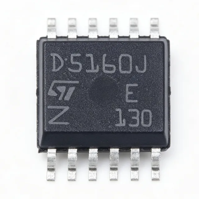
VND5160J-E - 16A High-Side Driver | STMicroelectronics | Automotive
The VND5160J-E is a monolithic high-side driver manufactured by STMicroelectronics, designed to drive resistive, inductive, and capacitive loads in automotive and industrial applications. It integrates a vertical MOSFET power stage with a full set of protection and diagnostic features in a compact PowerSSO-12 package. The device delivers a continuous output current of up to 16A (with proper thermal management) and operates from a supply voltage range of 4.5V to 36V, making it suitable for 12V and 24V automotive electrical systems. A high-side driver is a power management IC that connects a load to the positive supply rail, providing switching, protection, and diagnostic functions. It is a key component in automotive body control modules, where it replaces discrete relays and fuses with a more reliable, semiconductor-based solution. High-side drivers are part of the broader power management IC family, which includes low-side drivers, half-bridge drivers, and full-bridge drivers, all essential for controlling actuators, lamps, and motors in modern vehicles. Key features of the VND5160J-E include an output current limit of 16A, a low ON-state resistance (RDS(on)) of 60 mOhm typical at 25°C, and a standby current of only 5 µA. The device provides comprehensive protection against overcurrent, overtemperature, and short-circuit conditions, with an open-load detection feature for both ON and OFF states. It also includes a status output that reports fault conditions to the microcontroller, enabling real-time diagnostics. The PowerSSO-12 package offers excellent thermal performance with a thermal resistance of 40°C/W, allowing high-current operation without external heatsinking in many applications. The VND5160J-E is built using STMicroelectronics' VIPower M0-5 technology, which combines a vertical MOSFET with CMOS control logic on a single chip. This integration reduces component count and improves reliability compared to discrete solutions. The device is AEC-Q100 qualified, ensuring it meets the stringent quality and reliability requirements of the automotive industry. Its wide operating temperature range of -40°C to +150°C makes it suitable for under-hood and engine compartment applications. Typical applications include automotive body control modules for driving exterior and interior lighting, resistive heaters, and small DC motors. It is also used in industrial automation for controlling solenoids, valves, and actuators. The device's low standby current and robust protection features make it ideal for always-on applications in battery-powered systems. When designing with the VND5160J-E, ensure adequate PCB copper area for heat dissipation, especially when driving currents above 10A. The status pin should be connected to a microcontroller input with a pull-up resistor to enable fault detection. Proper decoupling capacitors on the supply and output pins are essential to minimize voltage transients during switching.
VND5E160AJTR-E - 7A High-Side Driver, VIPower M0-5, PowerSSO-12 | ST
The STMicroelectronics VND5E160AJTR-E is a single-channel high-side power switch / driver manufactured in ST's proprietary VIPower M0-5 technology and housed in the compact PowerSSO-12 surface-mount package. It is rated for 7 A continuous output current and is designed to drive 12 V automotive grounded loads while providing protection, diagnostics, and a 3 V / 5 V CMOS-compatible logic interface to any microcontroller. What is a high-side driver? A high-side driver is a type of smart power switch that sits between the battery/positive supply rail and the load, replacing discrete MOSFETs, fuses, and relay combinations. It belongs to the broader family of power switches / intelligent power switches (IPS) within the power management IC category, providing load protection, current sensing, and fault feedback to the microcontroller. Key features include 7 A continuous drain current (I_Load), 28 V operating supply range (V_CC), an integrated analog current-sense output (I_SENSE pin) proportional to load current, and built-in protections for load-dump, reverse-battery, over-temperature, short-circuit, and over-current conditions. The 3 V / 5 V CMOS-compatible input enables direct connection to modern microcontrollers without level shifters, simplifying the BOM in body and chassis control modules. The VIPower M0-5 process combines a vertical N-channel power MOSFET with analog and digital control blocks on the same die, enabling accurate current sensing (typically K_ILIS sense ratio) and robust switching. An exposed-pad PowerSSO-12 layout provides a low thermal resistance path (~5 °C/W junction-to-tab) for dissipating the I²R losses of 12 V automotive switching. Typical applications include automotive body modules for resistive and inductive loads such as lamps, LED arrays, motors, solenoids, and heaters, as well as industrial 24 V systems where reverse-battery and load-dump protection are required. The analog current-sense output also supports predictive maintenance by enabling MCU-side load-current monitoring. When designing with this part, place it as close as possible to the connector it is switching, and keep the protected load loop area minimal to reduce EMI from the 12 V bus. A small TVS across V_CC and an RC snubber on the output may be required for highly inductive loads such as solenoids or DC motors. This page synthesizes distributor pricing, same-brand drop-in alternatives such as the VND5E160JTR-E and VND5E160AJ-E, and practical design notes not consolidated on a single manufacturer or distributor page.
VND7004AYTR - 4A High-Side Driver with MultiSense | STMicroelectronics
The VND7004AYTR is a monolithic double channel high-side driver manufactured by STMicroelectronics using the proprietary VIPower M0-7 technology and housed in a PowerSSO-36 package. It is designed to drive 12 V automotive grounded loads through a 3 V and 5 V CMOS-compatible interface, providing protection and diagnostics. The device integrates advanced protective functions such as load current limitation, overload latch-off, thermal shutdown, and loss of ground protection, making it a robust solution for harsh automotive and industrial environments. A high-side driver is a type of power switch that connects a load to the positive supply rail, providing protection and diagnostic functions. It is a key component in automotive and industrial systems where loads such as lamps, relays, solenoids, and motors must be controlled safely. High-side drivers are part of the broader category of power management ICs, which manage the distribution and control of electrical power in electronic systems. The VND7004AYTR integrates advanced protection features including load current limitation, overload protection, thermal shutdown, and loss of ground protection, making it a robust solution for harsh environments. Key features of the VND7004AYTR include a 3V to 5V logic-level input compatible with microcontrollers, a standby current of only 0.5 µA (typ) to preserve battery life, and a fast demagnetization of inductive loads to reduce switching losses. The device also provides a status output for diagnostic feedback, enabling real-time monitoring of load conditions. Its low ON-state resistance and high current capability make it suitable for driving high-power loads without external heatsinks in many applications. The VND7004AYTR is built using STMicroelectronics' VIPower M0-7 technology, which integrates the power MOSFET with control and protection circuitry on a single chip. This monolithic approach reduces component count, improves reliability, and simplifies PCB layout. The device is fully protected against short circuits, overcurrent, and overtemperature, ensuring safe operation under fault conditions. Its fast switching performance and low quiescent current make it ideal for battery-operated and energy-efficient systems. Typical applications include automotive body control modules, lighting systems, industrial PLCs, and general-purpose power switching. In automotive applications, the VND7004AYTR can drive headlamps, wiper motors, and heating elements, while in industrial settings it can control solenoids, valves, and DC motors. The device's wide supply voltage range and robust protection make it a versatile choice for both 12V and 24V systems. When designing with the VND7004AYTR, ensure adequate PCB copper area for thermal dissipation, especially when driving continuous high currents. The exposed pad of the PowerSSO-36 package should be soldered to a large ground plane to minimize thermal resistance. Additionally, place a 100 nF ceramic capacitor close to the VCC pin to suppress voltage transients and ensure stable operation.
VND7040AJTR - 40A High-Side Driver | STMicroelectronics | Automotive
The VND7040AJTR is a double-channel high-side driver from STMicroelectronics, designed for automotive and industrial applications requiring robust power switching. It features a maximum output current of 40A, an operating voltage range of 4V to 28V, and is housed in a PowerSSO-16 package. The device integrates advanced protection features including overvoltage, undervoltage, overcurrent, and thermal shutdown, ensuring reliable operation in harsh environments. A high-side driver is a type of power switch that connects a load to the positive supply rail. It is commonly used in automotive systems to control lamps, motors, and solenoids, where the load must be switched on the high side for safety and diagnostic reasons. High-side drivers are part of the broader category of power management ICs, which manage and distribute power within electronic systems. Key features of the VND7040AJTR include a low quiescent current of 50 µA, a standby current of 5 µA, and a fast switching speed with rise and fall times of 10 µs and 15 µs, respectively. The device also provides a diagnostic output for fault detection, making it suitable for smart power distribution in automotive body control modules. The VND7040AJTR uses a proprietary VIPower M0-5 technology, which integrates the power MOSFET and control circuitry on a single chip. This technology ensures high efficiency and low power dissipation, with a typical on-resistance of 40 mΩ at 25°C. The device is AEC-Q100 qualified, meeting the stringent reliability standards for automotive electronics. Typical applications include automotive lighting control, DC motor driving, and power distribution in body control modules. The device's wide operating voltage range and robust protection features make it ideal for 12V and 24V automotive systems, as well as industrial PLCs and factory automation. When designing with the VND7040AJTR, it is essential to consider thermal management. The PowerSSO-16 package has a thermal resistance of 40°C/W, so adequate PCB copper area or a heatsink is required for high-current applications. Additionally, proper decoupling capacitors should be placed close to the supply pins to minimize voltage transients.
VND7050AJTR - Dual 70mOhm High-Side Driver | STMicroelectronics
The VND7050AJTR is a dual-channel high-side driver from STMicroelectronics, designed for automotive and industrial applications requiring robust power switching. It integrates two 70mOhm (typical) N-channel power MOSFETs with full protection and diagnostic features, housed in a PowerSSO-16 package. The device operates over a wide supply voltage range of 4V to 28V, making it suitable for 12V and 24V systems. Each channel can deliver up to 9A of continuous current, with a maximum current limitation of 14A (typical). The driver features an active-low enable input, open-drain diagnostic output, and built-in protection against overcurrent, overtemperature, and short-circuit conditions. A high-side driver is a power management IC that switches power to a load connected to ground, commonly used in automotive body control modules, industrial PLCs, and lighting systems. It integrates the power MOSFET, protection circuitry, and diagnostic feedback into a single package, simplifying PCB design and improving reliability. High-side drivers are part of the broader power management IC family, which includes low-side drivers, half-bridge drivers, and full-bridge drivers. The VND7050AJTR belongs to the VIPower M0-5 technology family, which is known for its low quiescent current and advanced protection features. Key features of the VND7050AJTR include a very low standby current of 0.5uA (typical) when disabled, which is critical for battery-powered automotive applications. The device also provides a diagnostic output that indicates open-load, short-to-ground, and overtemperature conditions. The PowerSSO-16 package offers excellent thermal performance with a thermal resistance of 40C/W (junction-to-ambient), enabling high-current operation without external heatsinks in many applications. The driver is AEC-Q100 qualified, ensuring reliability in harsh automotive environments. Technically, the VND7050AJTR uses a vertical N-channel power MOSFET architecture with a charge pump to drive the high-side switch. The charge pump allows the device to operate with a low input voltage while maintaining a low on-resistance. The device includes a current sense output that provides a proportional current signal for load monitoring, enabling precise control and diagnostics. The protection circuitry includes overvoltage clamping, reverse battery protection (with external resistor), and thermal shutdown with automatic restart. Typical applications include automotive body control modules for driving exterior lights, interior lighting, and DC motors; industrial PLCs for controlling solenoids and relays; and general-purpose power switching in 12V/24V systems. The VND7050AJTR is also suitable for driving resistive, capacitive, and inductive loads, making it a versatile choice for many power switching applications. When designing with this device, ensure adequate PCB copper area for thermal dissipation, especially when driving high currents. The diagnostic output should be connected to a microcontroller input with a pull-up resistor. For inductive loads, an external freewheeling diode is recommended to clamp voltage spikes during turn-off.
VND7140AJTR - Dual High-Side Driver 8A | STMicroelectronics | Automotive
The VND7140AJTR is a double channel high-side driver manufactured by STMicroelectronics using the proprietary VIPower M0-7 technology. It is housed in a PowerSSO-16 package and designed to drive 12V automotive grounded loads through a 3V and 5V CMOS-compatible interface. The device delivers up to 8A per channel and integrates advanced protective functions including load current limitation, overload active management by power limitation, and overtemperature shutdown with configurable latch-off. A high-side driver is a power management IC that connects a load to the positive supply rail, providing switching, protection, and diagnostic functions. In automotive systems, high-side drivers are essential for controlling lamps, solenoids, motors, and resistive loads while offering protection against short circuits, overcurrent, and overtemperature conditions. The VND7140AJTR belongs to the family of smart power switches, which combine power MOSFET technology with control and protection circuitry on a single chip. Key features of the VND7140AJTR include a MultiSense analog feedback pin that provides multiplexed analog feedback of load current with high precision proportional current mirror, VCC supply voltage, and TCHIP device temperature. This enables precise diagnostics and monitoring of the load condition. The device also features a FaultRST pin that unlatches the output in case of fault or disables the latch-off functionality, allowing flexible fault management. The PowerSSO-16 package offers excellent thermal performance with an exposed pad for efficient heat dissipation. The VND7140AJTR is designed for automotive applications and is AEC-Q100 qualified, ensuring reliability under harsh operating conditions. The device operates over a wide input voltage range and provides robust protection against load dump, reverse battery, and electrostatic discharge. The MultiSense feedback allows the microcontroller to read the load current, supply voltage, and device temperature, enabling advanced diagnostic and predictive maintenance capabilities. Typical applications include automotive body control modules, lighting control, DC motor control, and resistive load driving. The device is also suitable for industrial applications requiring high-side switching with diagnostic feedback. The VND7140AJTR is available in tape and reel packaging with a standard quantity of 1000 units per reel. When designing with the VND7140AJTR, ensure proper thermal management by connecting the exposed pad to a large copper area on the PCB. The MultiSense pin should be connected to an ADC input of the microcontroller for accurate current and temperature monitoring. The FaultRST pin can be used to implement latch-off or auto-restart fault handling depending on the application requirements.

VNI4140K-32 - Quad High-Side Smart Power SSR 1A PowerSSO-24 | STMicroelectronics
The STMicroelectronics VNI4140K-32 is a monolithic quad high-side smart power solid-state relay manufactured in ST's VIPower technology, designed to drive four independent resistive, capacitive, or inductive loads with one side connected to ground. Each channel delivers up to 1.0 A continuous current and integrates very low on-state resistance (RDS(on) of 0.08 ohm per channel), independent per-channel diagnostic feedback, and fast demagnetization of inductive loads in a 24-pin PowerSSO package with an exposed thermal pad. A high-side smart power switch (also called a high-side driver or smart solid-state relay) sits between the supply rail and the load; it replaces electromechanical relays with a semiconductor switch that can be commanded by logic-level signals. Within the broader taxonomy, the VNI4140K-32 belongs to the family of power management ICs (PMIC), specifically to the load-driver / smart-power-switch subcategory, which sits above discrete MOSFETs in functional integration and below complete PLC output modules in system scope. The IC integrates a vertical power MOSFET, gate driver, current-limit, thermal protection, and open-drain diagnostic on each of four channels in one package. Key specifications include a load current rating of 1.0 A per channel (limited to 0.6 A in the closely-related VNI4140K variant), a maximum supply voltage of 41 V, per-channel RDS(on) of 0.08 ohm, conformal to IEC 61131-2 for industrial PLC outputs, and ESD robustness rated per IEC air-discharge standards at 25 kV. Each channel independently reports open-load, short-to-ground, and over-temperature faults, and the fast demagnetization path handles the back-EMF of inductive loads without external freewheeling diodes. The VIPower M0 technology combines a vertical DMOS output stage with CMOS/bipolar control logic on the same die, allowing the integration of protection and diagnostic features around a power transistor. The exposed-pad PowerSSO-24 package provides a low junction-to-ambient thermal resistance, which is critical when all four channels conduct simultaneously: at full 1 A per channel, the total package dissipation can approach several watts and requires PCB copper-area heatsinking. Typical applications include 24 V PLC digital outputs (IEC 61131-2 compliant), industrial solenoid and valve drivers, automotive body controllers (lighting, relay substitution, ground-referenced loads), and any multi-channel resistive/inductive load switching where diagnostic feedback is required. The four independent channels are well suited to driving lamps, relays, LEDs, heaters, and small DC motors in parallel-bussed architectures. A key design consideration is the proximity between input and output on each channel: use a star-ground topology for the load returns and place the device close to the connector. The diagnostics only function correctly when the channel is fully on or fully off; PWM operation above a few hundred hertz should be validated against the channel's switching-loss budget. The exposed pad MUST be soldered to a sufficiently large copper pour to keep the junction temperature within the safe operating area. This page synthesizes distributor pricing from DigiKey/Mouser/Octopart, drops-in alternatives sourced from ST's VIPower portfolio, and practical design guidance not duplicated in the manufacturer datasheet.
VNI4140KTR-32 - Quad 1A High-Side SSR, 41V, PowerSSO-24 | STMicroelectronics
The STMicroelectronics VNI4140KTR-32 is a monolithic quad-channel high-side solid-state relay (SSR) fabricated in ST's VIPower technology, delivering up to 1 A continuous current per channel in a thermally-enhanced PowerSSO-24 package with an exposed bottom pad. Each of the four channels integrates an N-channel power MOSFET, a charge pump gate driver, per-channel diagnostic logic, and comprehensive protection circuitry. The device operates from a 10.5 V to 36 V supply and features a typical R_DS(on) of 0.08 ohm per channel, enabling direct drive of resistive, inductive, or capacitive loads connected to ground. A high-side solid-state relay is a semiconductor switch that replaces mechanical relays by using power MOSFETs to switch DC loads, offering silent operation, long life, fast switching, and built-in protection. The VNI4140KTR-32 sits in the power distribution hierarchy as a smart high-side driver, which is a category of power management IC that combines a switching element, gate drive, and diagnostic feedback in one device for industrial automation, body electronics, and IEC 61131-2 compliant PLC outputs. Key features include very low on-resistance (0.08 ohm typ), 1 A per-channel continuous current, integrated fast demagnetization of inductive loads, configurable latched or self-resetting thermal shutdown, per-channel open-load detection, short-circuit and overcurrent protection, and under-voltage lockout. The exposed bottom pad delivers a Rth(JA) suitable for 1 A operation on a standard 4-layer PCB without heatsinking. Typical applications include four-channel industrial PLC digital outputs (IEC 61131-2), programmable logic controller field-side switches, industrial sensor power distribution, building automation relay replacement, and multi-channel 24 V solenoid/valve drivers. Each channel can replace an electromechanical relay with PCB-friendly footprint and silent operation. Designers should ensure the charge pump bypass capacitor is placed as close to the VCC and GND pins as possible, route each output channel separately to minimize cross-talk, and use the exposed pad as the primary thermal path. The diagnostic output pin (DIAG) is multiplexed across channels and should be read in time-slotted fashion to identify the faulting channel during commissioning.

VNL5050S5-E - 19A Low-Side OMNIFET III Driver | STMicroelectronics
The STMicroelectronics VNL5050S5-E is a monolithic low-side power switch built on ST's VIPower (Vertical Intelligent Power) technology, delivering up to 19 A continuous drain current in an 8-pin SOIC package. It is the SOIC-8 sibling of the VNL5050N3-E SOT-223 variant and belongs to the OMNIFET III fully protected low-side driver family. The device integrates an N-channel power MOSFET with a 50 mOhm typical on-state resistance and a wide 3.5 V to 5.5 V logic supply range, accepting standard 3.3 V and 5 V microcontroller GPIO inputs without level shifting. A low-side power switch (also called a low-side driver or low-side MOSFET switch) is a discrete-or-circuit building block that sits between the load and ground. By switching the ground return path, it controls current flow through loads whose high side is tied to the battery. Compared with high-side switches, low-side drivers are simpler, lower on-resistance, and cheaper, at the cost of breaking the load's ground reference. The VNL5050S5-E sits in the broader hierarchy: power switch -> load driver -> power management IC -> semiconductor. Key features include ESD protection, integrated overvoltage clamp, thermal shutdown, current and power limitation, very low standby current, and very low electromagnetic susceptibility. Together these protections eliminate the need for external freewheeling diodes on inductive loads and remove most external snubber components, reducing BOM cost and PCB area. The OMNIFET III family is qualified for automotive AEC-Q100 environments, making this part usable in body electronics, junction boxes, and ECU driver stages. The architecture uses a vertical DMOS output stage co-packaged with CMOS logic and analog protection blocks on a single die. The protection chain monitors junction temperature, drain current, and VDS, and latches or cycles the output as needed. Logic inputs are TTL/CMOS compatible and include internal pull-down to keep the output off during MCU reset or floating conditions, simplifying firmware bring-up. Typical applications include automotive body controllers, relay replacement, solenoid and valve drivers, LED string grounding, and small DC motor drivers. The integrated protections make it suitable for harsh environments where discrete MOSFETs would require extensive external circuitry. With the 8-SOIC footprint, the part can be placed on the same pads as many legacy bipolar Darlington switches. When designing with the VNL5050S5-E, ensure the load is truly referenced to battery+ and that ground-referenced sensors downstream are not affected. For inductive loads above 1 mH, verify the internal avalanche clamp energy rating is within SOA using E = 0.5 * L * I^2, and consider an external TVS if load energy exceeds the internal clamp rating. This page synthesizes distributor pricing, drop-in alternatives, and practical design notes not found in the manufacturer datasheet alone.
VNQ500PEP-E - Quad Channel 500mA High-Side Driver | STMicroelectronics
The STMicroelectronics VNQ500PEP-E is a monolithic quad-channel high-side power switch driver fabricated in ST's proprietary VIPower M0-3 technology, housed in a 12-pin PowerSSO-12 (PowerSO-12) package with exposed pad. Each of the four independent channels delivers up to 500 mA continuous load current from a 4.5 V to 36 V supply rail, with CMOS-compatible inputs, integrated current limitation, shorted-load protection, overtemperature shutdown, undervoltage lockout, and loss-of-ground protection. A common chip-enable pin allows all four channels to be switched together for standby control. A high-side driver (HSD) is a type of power switch whose MOSFET drain is tied to the positive supply and source is tied to the load, in contrast to a low-side driver where the switch sits between the load and ground. Within the broader taxonomy, the VNQ500PEP-E belongs to the smart power switch family, which combines a power MOSFET, gate driver, and protection logic into a single monolithic IC. This integration replaces discrete N-channel MOSFETs plus their protection circuitry, simplifying PCB layout and improving diagnostic capability for automotive and industrial loads. Key features highlighted by our separate datasheet include 36 V load-dump tolerant transient capability, 1.0 A typical per-channel current limit, and an on-resistance RDS(on) below the 200 mOhm range for efficient switching of resistive, inductive, and capacitive loads. The exposed thermal pad (EP) on the PowerSSO-12 package delivers theta-JA around 50 C/W on a standard 4-layer JEDEC EIA/JESD51 board, allowing all four channels to operate at rated current without external heatsinking in most automotive body-control applications. Typical applications include automotive body control modules driving lamps, relays, solenoids, and small motors, as well as industrial PLC output cards, HVAC actuator drivers, and any multi-channel low-power DC load control. Designers choose the VNQ500PEP-E when they need four independently-protected high-side channels in a single compact package with full diagnostic feedback. When laying out the PCB, tie the exposed pad (pin 2 on PowerSSO-12) to a continuous ground copper pour for lowest thermal resistance, and keep the logic inputs short and bypassed to avoid false triggering from load transients. Always verify the channel's per-pin current limit behavior against your worst-case inrush load, especially for capacitive or lamp loads.
VNQ500PEPTR-E - 4-Ch High-Side 36V Driver | STMicroelectronics
The STMicroelectronics VNQ500PEPTR-E is a quad-channel high-side MOSFET power switch driver built on the company's VIPower M0-3 smart-power process, housed in a 12-pin PowerSSO-12 (PowerLSOP with exposed pad) package. It is rated for a 5.5 V to 36 V supply input range, delivers up to 400 mA continuous current per channel (0.9 A peak per Arrow listing), and integrates a 0.5 ohm typical on-resistance (Ron) per output. A high-side driver (also known as a high-side switch) is a power-distribution topology in which the load is connected between the switch output and ground, while the switch sits between the positive supply rail and the load. This contrasts with low-side switching, which returns the load to the positive rail and switches the ground return. High-side switching is preferred wherever the load must remain at a defined ground potential (for safety, EMI, or fault-detection reasons) and is the canonical building block of automotive body modules, industrial PLCs, and USB/eFuse power rails. Key feature highlights include four independently controlled outputs, internal current-limit and thermal-shutdown protection, very low quiescent current in standby, and CMOS/TTL-compatible logic inputs. Each output is protected against overload, short-circuit, and ESD events per AEC-Q100 stress profiles. According to the STMicroelectronics VNQ500 product page, the part is designed for "driving any kind of load with one side connected to ground," which captures the broad applicability of the device across resistive, inductive, and capacitive loads. Typical applications include automotive body-control modules (lighting, door locks, mirror heaters), industrial PLC and sensor-driver stages, USB port power switching, relay replacement, and any system that requires multiple protected 12 V/24 V loads on one PCB. With 36 V load-dump tolerance, the device is well-suited to 12 V automotive rails that routinely see transient overvoltage events. When designing with this device, ensure the PCB thermal layout uses the exposed pad (EP) as the primary heat-dissipation path. For >200 mA continuous outputs, a copper-pour area of at least 1 square inch under the EP is recommended, since Ron losses scale with I² and rise rapidly above 300 mA per channel.

VNQ5050AKTR - 13A High-Side Driver | STMicroelectronics | Automotive
The VNQ5050AKTR is a monolithic high-side driver from STMicroelectronics, designed for automotive and industrial applications requiring robust power switching. It integrates a 13A (typical) high-side switch with an embedded N-channel power MOSFET, providing protection against overcurrent, overtemperature, and short-circuit conditions. The device operates from a supply voltage range of 4.5V to 36V, making it suitable for 12V and 24V automotive systems. It is housed in a PowerSSO-36 package, which offers excellent thermal performance and is optimized for surface-mount assembly. A high-side driver is a power management IC that connects a load to the positive supply rail, enabling safe and controlled switching of inductive, resistive, or capacitive loads. In automotive systems, high-side drivers are essential for driving lamps, solenoids, relays, and motors, providing diagnostic feedback and protection features that enhance system reliability. The VNQ5050AKTR belongs to the VIPower M0-5 family, which is known for its advanced protection and diagnostic capabilities. Key features of the VNQ5050AKTR include a very low ON-state resistance (RDS(on)) of 50 mOhm typical, which minimizes power dissipation and supports high current handling. It offers a wide operating voltage range, a standby current of only 5 uA, and a comprehensive set of protection features including load current limitation, thermal shutdown with auto-restart, and loss of ground protection. The device also provides a status output for diagnostic feedback, enabling real-time monitoring of load conditions. From a technical perspective, the VNQ5050AKTR utilizes ST's VIPower M0-5 technology, which integrates the power MOSFET with control and protection circuitry on a single chip. This integration reduces external component count and improves system reliability. The device supports PWM control up to 1 kHz, allowing for dimming or proportional control of loads. Its thermal shutdown feature protects the device and load from overtemperature conditions, while the current limitation prevents damage from short circuits. Typical applications include automotive lighting (headlamps, tail lamps, interior lights), resistive and inductive loads such as relays and solenoids, and motor control in body control modules. The device's robust protection and diagnostic features make it ideal for safety-critical automotive systems. In industrial settings, it can be used for PLC outputs, factory automation, and general-purpose power switching. When designing with the VNQ5050AKTR, ensure adequate PCB copper area for thermal dissipation, especially when driving high currents. The exposed pad on the PowerSSO-36 package should be connected to a large ground plane to improve thermal performance. Additionally, place a suitable capacitor close to the VCC pin to suppress voltage transients and ensure stable operation. This page synthesizes distributor pricing, drop-in alternatives, and practical design notes not found in the STMicroelectronics datasheet, providing engineers with a comprehensive resource for selecting and implementing the VNQ5050AKTR.
VNQ5050KTR-E - 13A Quad High-Side Driver | ST | Automotive
The STMicroelectronics VNQ5050KTR-E is a monolithic quad-channel high-side driver delivering up to 13A per channel in a PowerSSO-24 exposed-pad package, designed for automotive and industrial loads. It operates across a 4.5V to 36V supply range with 3.0V CMOS-compatible logic inputs, integrating four N-channel power MOSFETs with vertical current-flow structures on a single die. A high-side driver is a power switch that connects a load to the positive supply rail rather than to ground, providing protection, diagnostics, and PWM capability. In the taxonomy of semiconductor switches, this places it under power MOSFET drivers -> smart power switches -> power management ICs -> semiconductor. High-side configuration is preferred in automotive body electronics because it allows the load to be referenced to chassis ground, simplifying wiring and enabling direct short-to-ground detection. Key features include a typical 13.5A per-channel current limit, 0.5 µA standby current for battery-saving key-off operation, very fast demagnetization of inductive loads via integrated freewheeling, and on-state / off-state open-load detection. The device also includes reverse-battery protection, loss-of-ground protection, overload protection with active power limitation, and thermal shutdown. The status flag pin multiplexes diagnostic information back to the host MCU. Built on ST's VIPower M0-5 technology, the VNQ5050KTR-E combines vertical power MOSFETs with bipolar/CMOS/DMOS control and protection circuitry monolithically. The embedded charge pump drives the gate above VCC, supporting 100% duty-cycle operation at low battery voltages. The architecture is engineered for harsh automotive environments including load-dump transients (tested per ISO 7637) and jump-start conditions. Typical applications include automotive lighting (headlamps, tail lamps, turn signals), body control modules driving solenoids and DC motors, and industrial programmable logic controllers switching relays. The quadruple channel fits the four-lamp-per-rear-lamp-cluster topology used widely in passenger cars. The exposed thermal pad of the PowerSSO-24 package must be soldered to a substantial PCB copper area to maintain junction temperature under full-load conditions, especially when all four channels are active simultaneously.
VNQ5160KTR-E - Quad High-Side Driver, 16A, 36V | STMicroelectronics
The STMicroelectronics VNQ5160KTR-E is a monolithic quad high-side driver designed for automotive and industrial resistive, inductive, and capacitive loads. It integrates four independent high-side switches with a 16A maximum output current per channel and an operating voltage range of 4.5V to 36V. The device is housed in a PowerSSO-24 package, providing a compact solution for multi-channel load switching. A high-side driver is a power management IC that connects a load to the positive supply rail, providing protection and diagnostic functions. In automotive systems, high-side drivers are essential for controlling lamps, solenoids, motors, and heaters while offering short-circuit, over-temperature, and load-dump protection. The VNQ5160KTR-E belongs to the VIPower M0-5 family, which is known for its robustness and advanced protection features. Key features include a very low standby current of 0.5 uA, making it suitable for battery-powered applications. Each channel has an open-load detection, over-temperature shutdown with auto-restart, and a current-limited output. The device also provides a status output for diagnostic feedback, enabling microcontroller-based fault monitoring. The PowerSSO-24 package offers excellent thermal performance with a thermal resistance of 40 C/W, allowing high current operation without external heatsinking in many applications. The VNQ5160KTR-E uses a vertical P-channel MOSFET technology, which eliminates the need for a charge pump, reducing system complexity. The device is AEC-Q100 qualified, ensuring reliability in harsh automotive environments. Its 16A output capability and 36V maximum supply voltage make it suitable for driving high-power loads such as headlamps, DC motors, and heating elements. Typical applications include automotive body control modules, lighting control, motor control, and industrial PLC output stages. The device's built-in protection features reduce the need for external components, simplifying PCB design and improving system reliability. When designing with this device, ensure adequate PCB copper area for thermal dissipation, especially when driving multiple channels at high current. The status output should be connected to a microcontroller input for fault monitoring, and the input pins should be protected with series resistors to limit inrush current.
VNQ6004SA-E - Quad High-Side Driver, 4x 60mOhm | STMicroelectronics
The STMicroelectronics VNQ6004SA-E is a monolithic quad-channel high-side driver designed for automotive and industrial resistive, inductive, and capacitive loads. It integrates four 60 mOhm (typical) high-side switches with full protection and diagnostic features in a 24-pin PowerSSO-24 package. The device operates from a 4.5V to 36V supply voltage, making it suitable for 12V and 24V automotive systems. Each channel can deliver up to 8A of output current (limited by package thermal constraints), with a typical on-state resistance of 60 mOhm at 25°C. A high-side driver is a power management IC that connects a load to the positive supply rail, providing switching, protection, and diagnostic functions. It is a key component in automotive body control modules, industrial PLCs, and smart power distribution systems. The VNQ6004SA-E belongs to the VIPower M0-5 family, which integrates power MOSFETs with control logic and protection circuits on a single chip, reducing external component count and improving reliability. Key features include overcurrent protection with programmable current limitation, thermal shutdown with automatic restart, undervoltage and overvoltage lockout, and open-load detection in both on and off states. The device also provides a status feedback pin for each channel, enabling real-time diagnostics. The PowerSSO-24 package offers excellent thermal performance with an exposed pad, allowing efficient heat dissipation in high-current applications. The VNQ6004SA-E uses ST's VIPower M0-5 technology, which combines a vertical power MOSFET with CMOS control logic. This architecture provides low on-resistance, fast switching, and robust protection. The device is AEC-Q100 qualified, ensuring reliability in harsh automotive environments. It also complies with RoHS and REACH directives, making it suitable for global markets. Typical applications include automotive body control modules (lighting, wipers, heaters), industrial PLC output stages, and smart power distribution in trucks and buses. The wide input voltage range and robust protection make it ideal for driving lamps, solenoids, relays, and DC motors. In automotive lighting, the VNQ6004SA-E can drive LED modules with PWM dimming, while its diagnostic features enable fault detection in safety-critical systems. When designing with this device, ensure adequate PCB copper area for thermal management, especially when driving high currents. The exposed pad must be soldered to a thermal via array to maximize heat dissipation. Also, consider the inrush current of capacitive loads and set the current limit accordingly to avoid false triggering.
VNQ6008SA-E - 8-Channel High-Side Driver | STMicroelectronics
The VNQ6008SA-E is a monolithic 8-channel high-side driver from STMicroelectronics, designed for automotive and industrial resistive, inductive, and capacitive loads. It integrates eight power MOSFETs with a 60V breakdown voltage and a typical on-state resistance of 60 mΩ per channel, enabling efficient switching of loads up to 1A per channel. The device is housed in a PowerSSO-36 package, providing a compact solution for multi-channel switching applications. A high-side driver is a type of power switch that connects a load to the positive supply rail, providing protection and diagnostic features. In automotive systems, high-side drivers are essential for controlling lamps, relays, solenoids, and other actuators while offering short-circuit, over-temperature, and over-voltage protection. The VNQ6008SA-E belongs to the VIPower M0-5 family, which is known for its robustness and advanced protection features. Key features of the VNQ6008SA-E include an 8-bit serial peripheral interface (SPI) for control and diagnostics, a 60V operating voltage range, and a low quiescent current of 5 µA in standby mode. Each channel has independent over-current, over-temperature, and open-load detection, with a diagnostic output that can be read via SPI. The device also features a dedicated current sense output for analog load monitoring, enabling precise current measurement without additional components. The VNQ6008SA-E utilizes ST's VIPower M0-5 technology, which combines vertical current flow with a smart power IC architecture. This technology provides high current density, low on-resistance, and fast switching, while integrating protection and diagnostic circuits on the same die. The device is AEC-Q100 qualified, making it suitable for automotive applications, and is RoHS compliant. Typical applications include automotive body control modules, lighting control (LED and incandescent lamps), relay and solenoid drivers, and industrial PLC output stages. The SPI interface allows for easy integration with microcontrollers, enabling real-time diagnostics and fault management. The device's ability to drive both resistive and inductive loads makes it versatile for various switching tasks. When designing with the VNQ6008SA-E, ensure proper thermal management by providing adequate copper area on the PCB for heat dissipation. The PowerSSO-36 package has a thermal resistance of 35 °C/W, so for high-current applications, consider the power dissipation and ambient temperature. Additionally, use appropriate decoupling capacitors on the supply and logic pins to minimize noise and ensure reliable operation.

VNQ660SP - 6A Quad High-Side Solid State Relay, PowerSO-10 | STMicroelectronics
The STMicroelectronics VNQ660SP is a monolithic quad-channel high-side solid state relay built on ST's VIPower M0-3 technology, delivering 6 A continuous current per channel in a 10-pin PowerSO-10 package. Each of the four independent N-channel MOSFET outputs exhibits a typical RDS(on) of 50 mΩ and is rated for a supply voltage (VCC) up to 36 V, with CMOS-compatible logic inputs driving the gates directly. A high-side solid state relay (also called a high-side driver or smart power switch) is an integrated power switch that sits between the supply rail and the load. Unlike a low-side switch that returns current to ground, a high-side switch delivers battery or bus voltage to the load, providing short-to-ground protection and removing the need for chassis-ground returns. Within the broader power semiconductor hierarchy, the VNQ660SP belongs to: smart power switch -> high-side driver -> power management IC -> semiconductor. The device integrates comprehensive protection features per channel, including off-state open-load detection, undervoltage and overvoltage shutdown, overvoltage clamping (active avalanche), thermal shutdown with auto-recovery, and current limitation. These diagnostics make it suitable for safety-critical automotive body electronics, where the part must survive load-dump transients and harsh wiring faults without external fuses. Architecturally, the VNQ660SP uses four independent vertical DMOS power stages with charge-pump gate drives that are powered from VCC. The charge pump keeps the gate enhanced at low VCC and during PWM operation, while the diagnostic block monitors load current and supply conditions to feed back to the microcontroller. The PowerSO-10 package exposes a metal pad that drops thermal resistance to a typical 1.5 °C/W, allowing the four channels to share heat dissipation when not all outputs are loaded simultaneously. Typical applications include automotive body control modules (BCM), door lock and window lift drivers, seat and mirror controllers, LED lighting modules, and industrial 24 V solenoid/valve banks. The combination of four channels, 6 A per channel, and integrated diagnostics is especially attractive in BCMs where PCB area is constrained and harness simplification matters. When designing with the VNQ660SP, derate per-channel current when more than two channels are conducting concurrently and follow PowerSO-10 land-pattern guidelines with thermal vias under the exposed pad. Always observe the maximum VCC of 36 V and add an external TVS if the upstream supply can produce larger transients. This page consolidates distributor pricing, true drop-in alternatives, and practical design notes that are not found in the manufacturer datasheet, giving engineers a single source for sourcing, replacement, and layout decisions on the VNQ660SP.