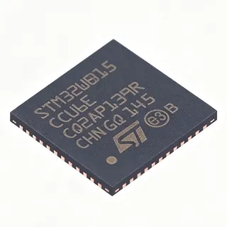
SI4123-D-GMR - Dual-Band RF Synthesizer | Skyworks (Tape & Reel)
MPN: SI4123-D-GMR ✗ کۆتایی ژیانSI4123-D-GMR گشتی
A frequency synthesizer generates a stable, programmable output signal by combining a phase-locked loop with a voltage-controlled oscillator. An RF synthesizer extends this function into the radio-frequency domain and is used to establish carrier or intermediate-frequency signals in wireless receivers, transmitters, and related communication equipment. The SI4123 family is positioned as a low-power, price-sensitive solution for personal wireless communications.
The SI4123-D-GMR integrates the VCO functions, which the Skyworks product description says reduces the external passive-component count and eliminates external VCOs and varactor diodes. This integration can simplify RF board layouts and reduce assembly requirements. Its dual-band capability allows one device family to address multiple wireless frequency plans, while programmable synthesis gives system designers flexibility in setting the generated frequency.
Typical wireless communication uses include RF front-end signal generation, intermediate-frequency synthesis, and dual-band transceiver support. The 2.7 V to 3.6 V supply range is suitable for low-voltage RF systems, while the listed 18 mA to 27 mA current range should be checked against the actual operating mode and frequency plan. The exposed-pad package also requires attention to PCB thermal dissipation and layout quality.
Designers should follow the manufacturer datasheet for the complete pinout, recommended loop-filter components, reference-clock requirements, RF output matching network, and decoupling layout. The available search results identify the device as obsolete or associated with an obsolete product status in comparison pages, so lifecycle confirmation should be completed before new production sourcing. This page consolidates verified distributor results, cross-reference findings, package information, application context, and engineering cautions.
جێگرەوەکانی جێگۆڕکێ بۆ SI4123-D-GMR — هەمان پاکەت، پین بە پین گونجاو. ئەو بەشانەی پاکەتی جیاوازیان هەیە و پێویستیان بە چاککردنەوەی PCB هەیە لابراون.
جۆرەکان لەم زنجیرەیەدا
مۆدێلەکانی هەمان زنجیرە کە بە شێوەی ڕاستەوخۆ گونجاون لەگەڵ SI4123-D-GMR (هەمان شێوە و پێکهاتەی شوێن) — جیاوازە لە Package, Mounting Type, Integrated VCOs, Manufacturer, Number of Circuits.
هیچ جێگرەوەی ڕاستەوخۆ بۆ ئەم بەرهەمە بەردەست نییە.
داوای جێگرەوەکان بکەSI4123-D-GMR تایبەتمەندییەکان
| Product Type | Dual-band RF frequency synthesizer |
| Integrated VCOs | Integrated VCOs |
| Frequency Range 1 | 900 MHz to 1800 MHz |
| Frequency Range 2 | 750 MHz to 1500 MHz |
| Supply Voltage Range | 2.7 V to 3.6 V |
| ئێستای دابینکردن | 18 mA to 27 mA |
| Output Power | -14 dBm to +1 dBm |
| Harmonic Rejection | -26 dBc to -20 dBc |
| پاکێج | 28-pin VFQFN with exposed pad |
| Number of Circuits | 13 circuits |
| Application Category | Clock generators, PLLs, and frequency synthesizers |
| RF Application | Wireless personal communications |
| جۆری دامەزراندن | Surface mount |
| Manufacturer | Skyworks Solutions Inc. |
| دۆخی چرخەی ژیان | Obsolete |
ڕێنمایی ڕێکخستنی پینی SI4123-D-GMR 28-pin vfqfn with exposed pad
ڕێکخستنی پین بۆ SI4123-D-GMR (پاکێجی 28-pin vfqfn with exposed pad). ژمارەدانی پین، فەنکشنەکان و نەخشەکانی پەیوەندی لە داتاشیتی بەرھەمھێنەردا پێناسە کراون. سەرنجی بدە بۆ شوێنپێی ورد و ڕێنمایییەکانی لەحیمکردن.

هیچ داتای وردی پینئاوت بەردەست نییە بۆ SI4123-D-GMR.
سەرنج بدە بە داتاشیت بۆ ڕێکخستنی تەواوی پینەکان.
بەکارهێنانە باوەکان
SI4123-D-GMR گونجاوە بۆ 6 بەکارھێنانs: Wireless Transmitter RF Signal Generation, Wireless Receiver Intermediate-Frequency Synthesis, Dual-Band Radio-Frequency Front End, Low-Voltage Wireless Communication Module, RF Test and Measurement Signal Source, Legacy Wireless Product Maintenance.
Wireless Transmitter RF Signal Generation
The SI4123-D-GMR fits wireless transmitter designs that need programmable RF synthesis across the listed 750 MHz to 1500 MHz and 900 MHz to 1800 MHz ranges. Its integrated VCOs can remove external VCO and varactor assemblies, reducing the number of discrete RF components that must be assembled and tuned. Place the device with a controlled reference clock, a datasheet-approved loop filter, and an RF output matching network, then verify output power and unwanted-signal performance with the actual antenna and PA load.
پێشنیارکراو
Wireless Receiver Intermediate-Frequency Synthesis
Use the SI4123-D-GMR when a wireless receiver requires a stable programmable intermediate-frequency source. The dual-band synthesis capability provides flexibility for frequency plans that use different RF and IF regions, while the listed 2.7 V to 3.6 V supply range supports low-voltage receiver architectures. The RF section must be isolated from sensitive receiver paths, and the loop-filter and reference-clock components should be selected only after confirming tuning and phase-noise requirements in the manufacturer documentation.
پێشنیارکراو
Dual-Band Radio-Frequency Front End
The SI4123-D-GMR is suited to dual-band RF front-end subsystems where the radio must synthesize signals for more than one supported frequency region. Integration of the VCOs can simplify the front end and reduce external RF passive count, which is valuable when board area and assembly cost are constrained. The implementation should separate high-level RF routing from sensitive reference and control paths, and should be validated for channel accuracy, spurious signals, output power, and behavior across both listed bands.
پێشنیارکراو
Low-Voltage Wireless Communication Module
The 2.7 V to 3.6 V operating range and listed 18 mA to 27 mA supply-current range make the SI4123-D-GMR relevant to low-voltage wireless communication modules. Integration may reduce the external component count compared with a discrete VCO implementation, helping designers target compact RF hardware. Because the product is reported obsolete, new module designs should first confirm lifecycle availability and consider a qualified active alternative rather than committing solely to a legacy part.
پێشنیارکراو
RF Test and Measurement Signal Source
The SI4123-D-GMR can be evaluated as a programmable RF source for bench and subsystem testing where the required frequency lies within its listed bands. Its dual-band synthesis and integrated VCOs make it useful for generating repeatable local oscillator or intermediate-frequency signals during receiver and transmitter characterization. Measurement setups should account for output power variation, reference-clock stability, loop-filter behavior, package parasitics, and the need to calibrate cable and fixture losses.
پێشنیارکراو
Legacy Wireless Product Maintenance
Because the SI4123-D-GMR is identified as obsolete in the supplied cross-reference data, it may still be relevant to maintenance and repair of deployed wireless equipment. An identical-orderable replacement must be confirmed through manufacturer or authorized-channel records rather than inferred from a generic cross-reference tool. Before substitution, compare the complete pinout, VFQFN dimensions and exposed-pad connection, supply current, frequency bands, control signaling, RF output level, and lifecycle documentation.
پێشنیارکراو
داتای سەرچاوەی ئەندازیاری بۆ SI4123-D-GMR — بەراوردکردن، ڕێنمایی دیزاین و زانیاری پابەندبوون.
ڕێنمایی هەڵبژاردن
بەراوردکردن لەگەڵ جێگرەوەکان
| پارامەتر | ئەم بەرهەمە | SI4123-D-GMRR |
|---|---|---|
| Package | 28-pin VFQFN with exposed pad | 28-pin VQFN with exposed pad |
| Brand | Skyworks Solutions Inc. | Silicon Laboratories |
جیاکەرەوە سەرەکییەکان
- Integrated VCO architecture (بەراورد بەSI4123-D-GMRR)
- Dual-band frequency coverage (بەراورد بەSI4123-D-GMRR)
- Low-voltage wireless positioning (بەراورد بەSI4123-D-GMRR)
تێبینییەکانی دیزاین
Follow the manufacturer reference layout for the 28-pin VFQFN exposed-pad package. Keep RF output routing short and controlled, connect the exposed pad using the recommended thermal-via pattern, and keep the reference-clock and loop-filter paths away from sensitive RF nodes. Because the supplied data identifies an exposed-pad package, inspect the package drawing and land pattern before fabrication rather than relying only on the generic QFN name.
Design the 2.7 V to 3.6 V supply rail with local high-frequency decoupling and adequate transient response for the listed 18 mA to 27 mA operating-current range. Place bypass capacitors close to the supply and ground pins, verify startup behavior, and avoid noisy digital or switching-regulator coupling into the synthesizer reference and RF sections. Confirm the actual current at the intended frequency and output setting rather than sizing only from the headline range.
Validate phase noise, reference spurious signals, tuning accuracy, and output matching across the intended frequency bands. The supplied data gives broad frequency and output-power ranges but does not provide phase-noise or spur plots, so those requirements must be measured or obtained from the manufacturer. Use controlled impedance, short RF paths, and a defined RF load during prototype measurements.
Do not substitute a similarly named SI4123 variant without checking the complete pinout, package dimensions, exposed-pad connection, frequency range, supply limits, control interface, and RF output specification. The supplied comparison page describes SI4123-D-GMRR as potentially similar, but it does not provide complete verified parameter values. Treat cross-reference pages as leads for engineering review, not as proof of drop-in replacement.
زانیاری پابەندبوون
The supplied search snippets do not provide authoritative compliance declarations for this part. RoHS, REACH, lead-free, halogen-free, and conflict-minerals status should be confirmed from the manufacturer or authorized distributor documentation.