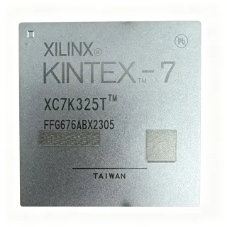
XC5VLX50-1FFV676C - Virtex-5 LX 50 FPGA with 440 I/O | AMD/Xilinx
MPN: XC5VLX50-1FFV676C ✗ کۆتایی ژیانXC5VLX50-1FFV676C گشتی
A field-programmable gate array is a semiconductor device whose logic functions are configured after fabrication. An FPGA integrates programmable lookup tables, flip-flops, programmable interconnect, block RAM, dedicated input/output resources, and other fixed-function blocks into one reconfigurable device. Within the product hierarchy, this component is an FPGA and CPLD-class programmable logic device, a digital semiconductor, and a configurable system-on-chip platform that can implement control logic, datapaths, protocol bridges, and signal-processing functions in one package.
The XC5VLX50 part is identified by the 50 device within the Virtex-5 LX family and is offered here in the XC5VLX50-1FFV676C ordering configuration. Its most prominent visible resource figures are 440 I/O, 1,769,472 logic cells, and 46,080 flip-flops. The -1 ordering suffix denotes the device speed designation, while FFV676C identifies the 676-ball FCBGA package and commercial temperature or qualification characteristics. The manufacturer and distributor listings identify the device as a Virtex-5 LX FPGA.
Compared with smaller programmable logic devices, the XC5VLX50 provides a large fabric for parallel datapaths and multi-module designs. Its 440 I/O count is particularly useful for systems requiring substantial external connectivity, such as parallel sensor aggregation, high-speed data capture, legacy peripheral interfaces, and test equipment. The 46,080 flip-flops support substantial sequential logic, while the 1,769,472 logic-cell figure provides capacity for wide combinational and parallel processing architectures.
Typical applications include telecommunications interface equipment, industrial control systems, high-speed data acquisition, instrumentation, networking equipment, embedded signal processing, and specialized accelerator logic. In a telecommunications design, the FPGA can combine multiple interface conversions and protocol functions in parallel. In industrial equipment, it can implement deterministic timing, acquisition control, and supervisory logic. In data-acquisition systems, its 440 I/O and programmable fabric can reduce the number of discrete interface devices required.
Design planning should begin with the exact 676-ball FCBGA footprint, power requirements, configuration method, supported I/O standards, and available board resources. Because this high-pin-count BGA package requires careful escape routing, power-plane design, thermal management, and assembly process control, use the manufacturer package drawings and device documentation for land patterns and ball assignments. The FFV package designation also requires careful review of thermal and supply-chain availability for the intended production program.
This page consolidates the exact resource and package figures, available same-package replacement information, practical implementation guidance, and a parameter-by-parameter engineering comparison. It helps designers identify where XC5VLX50-1FFV676C fits and where its high logic density, extensive I/O availability, or large package adds value over smaller FPGA options.
جێگرەوەکانی جێگۆڕکێ بۆ XC5VLX50-1FFV676C — هەمان پاکەت، پین بە پین گونجاو. ئەو بەشانەی پاکەتی جیاوازیان هەیە و پێویستیان بە چاککردنەوەی PCB هەیە لابراون.
جۆرەکان لەم زنجیرەیەدا
مۆدێلەکانی هەمان زنجیرە کە بە شێوەی ڕاستەوخۆ گونجاون لەگەڵ XC5VLX50-1FFV676C (هەمان شێوە و پێکهاتەی شوێن) — جیاوازە لە Package, Device Type, Logic Cells, Architecture, Lead-Free Status.
XC5VLX50-1FFG676C
✅ جێگرەوەی ڕاستەوخۆپەیوەندی بۆ نرخ
بینینی داتاشیت →XC5VLX50-1FFV676C زۆرترین ڕێژە و تایبەتمەندییە کارەباییەکان
| Device Type | Virtex-5 LX field-programmable gate array (FPGA) |
| Number of I/O | 440 I/O |
| Logic Cells | 1,769,472 logic cells |
| Flip-Flops | 46,080 flip-flops |
| پاکێج | 676-BBGA, FCBGA |
| Architecture | Second-generation ASMBL column-based architecture |
| FPGA Family | Virtex-5 LX |
| Product Series | Virtex-5 |
| Device Designator | XC5VLX50 |
| Speed Grade | -1 |
| Package Pin Count | 676 balls |
| جۆری دامەزراندن | Surface mount |
| دۆخی RoHS | RoHS non-compliant |
| Lead-Free Status | Contains lead |
ڕێنمایی ڕێکخستنی پینی XC5VLX50-1FFV676C 676 balls
ڕێکخستنی پین بۆ XC5VLX50-1FFV676C (پاکێجی 676 balls). ئەم IC ی دیجیتاڵە GPIO، ڕووکارەکانی پەیوەندی (UART، SPI، I2C) و پینی وزە لەخۆدەگرێت. سەرنج بدە بە داتاشیتی بەرھەمھێنەر بۆ فەنکشنەکانی پینی جێگرەوە و ھەڵبژاردنەکانی ڕێکخستن. پێویستە بۆ دیزاینی سیستەمی جێگیر و ڕێکخستنی PCB.

هیچ داتای وردی پینئاوت بەردەست نییە بۆ XC5VLX50-1FFV676C.
سەرنج بدە بە داتاشیت بۆ ڕێکخستنی تەواوی پینەکان.
بەکارهێنانە باوەکان
XC5VLX50-1FFV676C گونجاوە بۆ 6 بەکارھێنانs: Industrial Data Acquisition, Telecommunications Interface Equipment, High-Speed Signal Processing, Network Packet Processing, Test and Measurement Instrumentation, Embedded Control and System Interconnect.
Industrial Data Acquisition
The XC5VLX50-1FFV676C fits wide parallel data-acquisition systems where numerous sensors, counters, and memory interfaces must operate concurrently. Its 440 I/O provide substantial board-level connectivity, while 1,769,472 logic cells and 46,080 flip-flops support acquisition pipelines, trigger logic, calibration tables, and channel control without splitting the design across multiple devices. The 676-ball FCBGA supports dense routing of wide buses and high-speed memory interfaces. Designers should pair the FPGA with decoupling, clock distribution, controlled-impedance routing, and thermal vias under the exposed package area. The main consideration is assembly complexity: a 676-ball device requires a controlled BGA process and careful power and thermal planning.
پێشنیارکراو
Telecommunications Interface Equipment
The XC5VLX50-1FFV676C is suitable for telecommunications interface equipment that must combine multiple data paths and protocol functions in a single programmable device. Its 440 I/O can accommodate parallel payload, control, clock, and status connections, while the large logic fabric supports framing, multiplexing, buffering, and line-interface adaptation. The 1,769,472 logic cells allow independent channels to be implemented in parallel rather than time-multiplexed through a smaller device. For deployment, validate the required I/O standards, clock rates, power rails, and configuration method against the exact device documentation. Thermal analysis and multilayer PCB construction are especially important because both logic activity and high-speed I/O can concentrate heat around the large FCBGA.
پێشنیارکراو
High-Speed Signal Processing
The XC5VLX50-1FFV676C provides substantial parallel logic for filtering, correlation, FFT-style datapaths, and other fixed-point signal-processing pipelines. The 46,080 flip-flops support a large number of sequential processing stages, and the 1,769,472-cell fabric allows multiple lanes or channels to be implemented concurrently. Its 440 I/O also allows external converters, memory devices, and data-capture circuits to interface directly with the processing fabric. A practical design should use device-specific timing constraints, register pipelining, and dedicated clock resources to achieve repeatable throughput. Before layout, confirm the clocking architecture and I/O performance required by the target data rate because those detailed limits are not established by the basic resource listing.
پێشنیارکراو
Network Packet Processing
The XC5VLX50-1FFV676C can support network equipment requiring parallel packet classification, buffering, header parsing, and traffic-management functions. The large logic-cell and flip-flop counts allow multiple pipeline stages to coexist, while 440 I/O provide high connectivity to external memory, PHY devices, and backplane interfaces. Using the FPGA in this role avoids a strict processor-plus-discrete-logic split when the design can be expressed as deterministic parallel datapaths. Engineering attention should center on memory bandwidth, clock-domain boundaries, packet-buffer architecture, and I/O standards rather than logic-cell count alone. The 676-ball package offers routing flexibility for wide interfaces, although its power and assembly requirements are greater than those of smaller FPGA packages.
پێشنیارکراو
Test and Measurement Instrumentation
The XC5VLX50-1FFV676C fits instrumentation that requires extensive stimulus generation, response capture, timing control, and instrument-bus connectivity. Its 440 I/O can expose parallel measurement channels, while the 1,769,472 logic cells and 46,080 flip-flops support acquisition sequencing, pattern generation, correlation, and local processing. Consolidating these functions into one FPGA can simplify synchronization compared with a collection of separate programmable devices. The design must still account for analog isolation, calibration, signal integrity, and clock-jitter performance outside the FPGA. For the BGA implementation, use a stable reference clock, carefully filtered supplies, solid return paths, and thermal relief under the device. Exact pin functions and package geometry should be taken from the FFV package documentation.
پێشنیارکراو
Embedded Control and System Interconnect
The XC5VLX50-1FFV676C can act as a central programmable controller for industrial or embedded systems that need to bridge many peripherals while executing deterministic supervisory logic. Its 440 I/O supports combinations of serial links, parallel buses, discrete control signals, and memory interfaces, while the large fabric can absorb protocol adapters and real-time control functions. This consolidation can reduce inter-device communication latency and simplify board partitioning. Designers should define clock domains and reset strategy early, reserve I/O for the selected electrical standards, and avoid routing high-speed or noisy signals through general-purpose fabric. The 676-ball FCBGA requires a multilayer board with disciplined power distribution and thermal design, making this configuration most appropriate when its connectivity and logic capacity are genuinely required.
پێشنیارکراو
داتای سەرچاوەی ئەندازیاری بۆ XC5VLX50-1FFV676C — بەراوردکردن، ڕێنمایی دیزاین و زانیاری پابەندبوون.
ڕێنمایی هەڵبژاردن
بەراوردکردن لەگەڵ جێگرەوەکان
| پارامەتر | ئەم بەرهەمە | XC5VLX50-1FFG676C |
|---|---|---|
| Brand | AMD/Xilinx | AMD/Xilinx |
| Package | 676-BBGA, FCBGA | 676-BBGA, FCBGA |
| FPGA Family | Virtex-5 LX | Virtex-5 LX |
| Device Designator | XC5VLX50 | XC5VLX50 |
| Number of I/O | 440 I/O | 440 I/O |
| Logic Cells | 1,769,472 logic cells | 1,769,472 logic cells |
| Flip-Flops | 46,080 flip-flops | 46,080 flip-flops |
| Architecture | Second-generation ASMBL column-based architecture | Virtex-5 LX architecture; detailed comparative parameter not stated |
| Speed Grade | -1 | -1 |
| Pin Compatibility | 676-BBGA, FCBGA reference footprint | Pin-compatible with the same logic and package features |
جیاکەرەوە سەرەکییەکان
- Published core resource figures are unchanged in the documented replacement (بەراورد بەXC5VLX50-1FFG676C)
- Direct same-package procurement path (بەراورد بەXC5VLX50-1FFG676C)
- Large deterministic parallel-logic capacity (بەراورد بەXC5VLX50-1FFG676C)
تێبینییەکانی دیزاین
Treat the 676-ball FCBGA as a high-density routing and assembly constraint. Follow the manufacturer package drawing for ball locations, pad geometry, solder-mask design, and assembly process requirements. Route high-speed interfaces over continuous reference planes, minimize stubs, provide dense decoupling near the device, and confirm the board stack-up and impedance model against the selected I/O standards.
Provide a low-impedance power-delivery structure and thermal paths appropriate for the 676-ball package. Use multiple voltage planes or splitting where the device documentation calls for it, place decoupling capacitors close to supply and ground balls, and evaluate copper spreading around the package. Calculate worst-case dissipation from the actual design activity and verify junction-temperature limits before production release.
Preserve configuration access and implement a reliable startup path for this Virtex-5 LX device. Review the configuration pins, mode settings, clock, and reset requirements in the applicable device documentation before assigning PCB resources. Keep sensitive configuration or JTAG signals away from aggressive aggressors, provide the specified pull components, and test boundary-scan access after assembly.
زانیاری پابەندبوون
The XC5VLX50 family listing states RoHS non-compliant and contains lead. REACH, AEC-Q100, halogen-free, and conflict-minerals status are not established for the exact ordering code.