MC9S12C96CFUE vs MC9S12DJ128CPVE Comparison
Detailed side-by-side comparison of MC9S12C96CFUE by NXP Semiconductors and MC9S12DJ128CPVE by NXP Semiconductors. Compare key specifications, electrical parameters, packaging, lifecycle status, pricing, and availability to determine the best component for your design requirements.

NXP Semiconductors
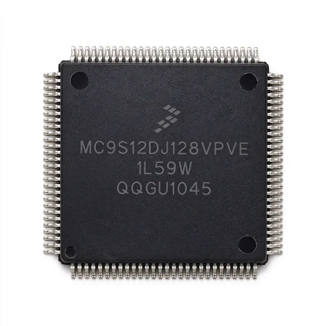
MC9S12DJ128CPVE - HCS12 16-bit MCU, 128KB Flash, 112-LQFP | NXP
MC9S12DJ128CPVE NrndSpecification Comparison
| Parameter | MC9S12C96CFUE | MC9S12DJ128CPVE |
|---|---|---|
| Brand | NXP Semiconductors | NXP Semiconductors |
| Category | Microcontrollers | Microcontrollers |
| Lifecycle Status | NRND | NRND |
| Stock Status | In Stock | In Stock |
| Unit Price (USD) | $0.00 | $19.75 |
| Product Type | 16-bit HCS12 microcontroller | — |
| CPU Core | HCS12 16-bit core | — |
| Data Bus Width | 16 bit | 16 bit |
| Maximum Clock Speed | 25 MHz | — |
| Flash Memory | 96 KB | — |
| Flash Organization | 96K x 8 bits | — |
| External Supply Range | 2.97 V to 5.5 V | — |
| Internal Regulator | On-chip bandgap-based Vreg | — |
| Clock Generation | Phase-lock loop (PLL) circuit | — |
| Package | 80-pin LQFP, 14 x 14 mm | 112-LQFP (20 x 20 mm) |
| Mounting Type | Surface mount | Surface Mount |
| Application Domains | Industrial and automotive network applications | — |
| Program Storage Type | Flash | — |
| Lifecycle Status | NRND | NRND (Not Recommended for New Designs) |
| I/O Port Count | [DATA_NEEDED: exact I/O port count] | — |
| RAM | [DATA_NEEDED: RAM capacity] | — |
| EEPROM | [DATA_NEEDED: EEPROM capacity] | — |
| Operating Temperature Range | [DATA_NEEDED: operating temperature range] | [DATA_NEEDED: -40C to +85C or -40C to +125C] |
| RoHS Status | [DATA_NEEDED: RoHS status] | [DATA_NEEDED: RoHS status] |
| REACH Status | [DATA_NEEDED: REACH status] | — |
| AEC-Q100 Qualification | [DATA_NEEDED: AEC-Q100 qualification] | — |
| Core | — | HCS12 |
| Maximum Clock Frequency | — | 25 MHz |
| Program Memory Size | — | 128 KB (128K x 8) Flash |
| RAM Size | — | [DATA_NEEDED: RAM size in bytes] |
| Supply Voltage Range | — | [DATA_NEEDED: VDD min/max] |
| SCI (UART) Interfaces | — | 2 |
| SPI Interfaces | — | 2 |
| I2C (Inter-IC Bus) Interfaces | — | 1 |
| ADC Channels | — | 2 x 8-channel, 10-bit |
| PWM Channels | — | 8 |
| Enhanced Capture Timer Channels | — | 8 (IC/OC) |
| Digital I/O Pins | — | 20 |