Produkte (32725)

VSP3200Y - 16-Bit 8MSPS CCD Signal Processor | TI
VSP3200Y

VSP3200Y - 16-Bit 8MSPS CCD Signal Processor | TI

The Texas Instruments VSP3200Y is a 16-bit, 8 MSPS, 3-channel analog front end (AFE) CCD signal processor with dual output mode, housed in a 48-pin LQFP (7x7 mm) package and operating from a single +5V supply. A CCD/CIS analog front end is the mixed-signal stage between an image sensor and a digital image processor. It samples tiny charge-derived pixel voltages, removes reset and kTC noise through correlated double sampling (CDS), amplifies the signal to match the ADC input range, and digitizes it. Within the signal chain hierarchy, the AFE sits between the sensor and the image-signal processor, and is a critical determinant of final image dynamic range and noise floor. Key features include an integrated triple correlated double sampler (CDS), a programmable gain amplifier with up to +13 dB gain, selectable operating modes (1-channel or 3-channel CCD mode at up to 8 MSPS), selectable normal or demultiplexed output modes, and an offset control range of +3V. The 16-bit conversion resolution preserves fine shadow detail in scanned images, essential for document and film scanners. Architecturally, the VSP3200 combines three CDS/PGA channels feeding a 16-bit ADC pipeline optimized for line-rate scanning. The demultiplexed output mode makes the device interface compatible with the VSP3210, which is pin-to-pin compatible with the VSP3100 in that mode, providing a migration path to a one-chip solution. Typical applications include flatbed document scanners, film scanners, CIS-based scanner modules, and industrial inspection cameras that use CCD or CIS sensors. Design consideration: because the part runs from a single +5V rail, keep the analog 5V supply clean and well decoupled; noise on this rail directly appears in pixel data at 16-bit resolution levels. This page synthesizes distributor pricing, drop-in alternatives, and practical design notes not found in the manufacturer datasheet.

USD $23,95 Auf Lager
VSP3200Y-2K - 16-Bit 8MSPS CCD Signal Processor | Texas Instruments
VSP3200Y-2K

VSP3200Y-2K - 16-Bit 8MSPS CCD Signal Processor | Texas Instruments

The Texas Instruments VSP3200Y-2K is a 16-bit, 8 MSPS, 3-channel analog front end (AFE) signal processor for CCD, CMOS, and CIS image sensors, housed in a 48-pin LQFP (7x7 mm) package and operating from a single +5V supply. An analog front end for image sensors is the circuit block between the imaging array and the digital image processor. It performs correlated double sampling (CDS) to remove reset noise and kTC noise from the CCD output, applies programmable gain to normalize signal amplitude across color channels, and digitizes the conditioned signal with a high-resolution ADC. Within the system hierarchy, the AFE sits inside the imaging signal chain: image sensor -> AFE (CDS + PGA + ADC) -> DSP/ASIC -> host interface. Key features of the VSP3200Y include three Correlated Double Samplers (CDSs) and three Programmable Gain Amplifiers (PGAs) that process CCD signals from 3-channel (RGB) scanners, a 16-bit conversion path running at up to 8 MSPS, dual output mode for flexible host interfacing, and single +5V operation that simplifies power tree design in desktop scanner platforms. Technically, the VSP3200Y integrates the complete analog processing chain for CCD signal conditioning: the CDS stages sample the pixel signal twice to cancel low-frequency drift and reset noise, the PGAs allow per-channel gain calibration, and the internal 16-bit ADC delivers 8 Msps throughput. Interface compatibility with the VSP3210 single-chip product, which is itself pin-to-pin compatible with the VSP3100 in demultiplexed output mode, provides a migration path for higher integration designs. Typical applications are flatbed and document scanners using CCD or CIS linear arrays, industrial inspection cameras, and desktop imaging peripherals that require 16-bit depth at moderate 8 MSPS speeds. A key design consideration is layout of the analog ground and the CCD output trace: keep the sensor-to-CDS input path short, guard it from digital output drivers, and provide a clean +5V rail with local decoupling, because residual reset noise not removed by the CDS directly limits the effective 16-bit resolution. This page synthesizes distributor inventory, drop-in alternatives, pricing tiers, and practical design notes not found in the manufacturer datasheet.

USD $8,40 Auf Lager
VSP3200Y-2KG4 - 16-Bit 8MSPS CCD Signal Processor | TI
VSP3200Y-2KG4

VSP3200Y-2KG4 - 16-Bit 8MSPS CCD Signal Processor | TI

The Texas Instruments VSP3200Y-2KG4 is a 16-bit, 8 MSPS 3-channel analog front end (AFE) signal processor for CCD, CMOS and CIS image sensors, housed in a 48-pin LQFP (7x7 mm) package and operating from a single +5 V supply over 0C to +85C. An analog front end for image sensors is a specialized data-conversion IC that sits between a charge-coupled device (CCD) sensor and the digital image pipeline. It performs correlated double sampling (CDS) to remove kTC and low-frequency noise, applies programmable gain, offsets the black level, and digitizes the conditioned pixel signal with a high-speed ADC, delivering a clean digital video stream to downstream DSP or image-processing logic. Key features of the VSP3200Y include three independent Correlated Double Samplers (CDS) and three Programmable Gain Amplifiers (PGAs) that process CCD signal channels end-to-end on one chip, a 16-bit ADC running at up to 8 MSPS, and dual output mode for flexible system interfacing. Integration of the complete analog chain eliminates discrete CDS/PGA stages, reducing board area and analog design risk. The device is built on CMOS process technology and provides a serial digital output interface. According to TI product documentation, the VSP3200Y is interface compatible with the VSP3210, a 16-bit one-chip product; the VSP3210 is in turn pin-to-pin compatible with the VSP3100 when operated in demultiplexed output mode, giving designers a documented upgrade and substitution path within the same LQFP-48 family. Typical applications include CCD camera signal chains for industrial inspection, consumer video capture, and contact image sensor (CIS) modules used in scanners and document imaging. The single 5 V supply suits legacy 5 V consumer and industrial boards. When designing with this part, verify power-supply decoupling on both the analog and digital domains and confirm the output mode (multiplexed vs dual) matches the pixel-rate timing of your CCD clocking scheme. This page synthesizes distributor availability, drop-in family alternatives (VSP3210, VSP3200Y, VSP3100), and design considerations not found on the manufacturer product page.

USD $13,40 Auf Lager
W24257AJ-20 - 32Kx8 20ns CMOS SRAM | Winbond DIP-28
W24257AJ20

W24257AJ-20 - 32Kx8 20ns CMOS SRAM | Winbond DIP-28

The Winbond W24257AJ-20 is a 32,768 x 8-bit high-speed CMOS Static RAM (SRAM) organized as 32K words by 8 bits, with a 20 ns maximum access time and housed in a 28-pin DIP (J-bend) through-hole package. It operates from a single +5 V power supply and is manufactured using Winbond's high-performance CMOS process, delivering low power dissipation typical of CMOS memory. A Static RAM is a type of volatile semiconductor memory that retains data bits as long as power is applied, with no refresh cycle required - in contrast to dynamic RAM (DRAM). SRAM belongs to the memory ICs family within the broader semiconductor hierarchy (SRAM -> volatile memory -> random-access memory -> integrated circuit -> semiconductor). The W24257AJ-20 is a fully asynchronous SRAM with standard JEDEC-compatible pinout for a 32K x 8 organization, allowing direct replacement of legacy 62256-type devices on existing PCBs. Key features of the W24257AJ-20 include a 20 ns access time (suitable for systems clocked up to 50 MHz without wait states), CMOS low standby current, fully static operation (no clock or refresh required), and TTL-compatible I/O levels. The device supports common memory-interface signals such as /CS1, CS2, /OE, and /WE, and provides three-state outputs for bus-oriented applications. The "AJ" suffix denotes the DIP-28 plastic package while "-20" specifies the 20 ns speed grade. Typical applications include legacy industrial controllers, point-of-sale terminals, firmware buffers for embedded microcontrollers, data-logging buffers, and as a working-memory expansion for older 8-bit and 16-bit microprocessor systems. The DIP-28 form factor is convenient for breadboarding, prototyping, and through-hole repair of legacy equipment. Because the part uses the standard 32K x 8 pinout, designers can upgrade older 8K x 8 or 32K x 8 SRAM sockets without any PCB rework. When designing with the W24257AJ-20, observe standard SRAM decoupling practice: place a 0.1 uF ceramic bypass capacitor close to the VCC pin and a bulk 10 uF capacitor on the supply rail. Avoid leaving inputs floating; tie unused /CS1 to VCC through a pull-up and unused /OE to GND to minimize ICC. The 20 ns grade is generally a drop-in replacement for slower 70-200 ns legacy SRAMs on the same PCB, but verify bus timing for high-MHz systems. This page synthesizes Winbond datasheet specifications, distributor stock signals, drop-in replacement candidates, and practical design notes not aggregated on any single distributor page.

USD $1,55 Auf Lager
W24512AKDV - 64Kx8 5V CMOS SRAM | Winbond
W24512AKDV

W24512AKDV - 64Kx8 5V CMOS SRAM | Winbond

The Winbond W24512AKDV is a 64K x 8 (512 Kbit) high-speed CMOS static RAM organized as 65,536 words of 8 bits, operating from a single 5V power supply. Fabricated on Winbond's high-performance CMOS process, the device offers industry-standard access times of 15/20/25/35 ns (per the W24512A datasheet family), low active power, and CMOS standby current, making it suitable for both high-performance and battery-aware designs. A static RAM (SRAM) is a type of volatile memory that stores each bit in a bi-stable latch, eliminating the need for periodic refresh cycles required by dynamic RAM. In the broader memory hierarchy, SRAM sits between ultra-fast register files and denser but slower DRAM/Flash. The 64K x 8 organization - eight data I/O lines and sixteen address lines - is the classic JEDEC-style parallel SRAM pinout that traces back to the original 6264-family 8K x 8 and is fully pin-compatible with modern asynchronous SRAMs. Key differentiating attributes include fully static operation (no clock or refresh required), TTL-compatible I/O, a chip-enable pin for memory expansion, and an output-enable pin for bus arbitration. The CMOS process delivers typical active currents in the tens of milliamps at full bus activity, with standby leakage dropping into the microamp range when CE is de-asserted - ideal for low-power embedded systems. Architecturally, the W24512AKDV uses a 6-transistor (6T) CMOS memory cell, which gives excellent noise immunity and stable read margins across temperature. The internal address decoders, write drivers, and sense amplifiers are optimized for sub-20 ns access at 5V, ensuring compliance with microprocessor and microcontroller bus timing without wait states in many cases. Typical applications include industrial controllers, data loggers, networking line cards using look-up tables, telecom buffers, point-of-sale terminals, and any embedded system needing byte-wide non-volatile cache/working memory paired with Flash. Engineers retrofitting legacy 5V designs or building new 5V-tolerant industrial equipment will find this part a direct mechanical and electrical substitute for older 6264-style SRAMs. When designing with this part, always place 0.1 uF decoupling capacitors close to VCC and VSS, and observe derating for output loading above 50 pF to stay within the 15/20/25/35 ns access-time envelopes. The CE pin must be pulled inactive for true standby current savings. This page synthesizes current distributor pricing, drop-in alternatives, and design notes not found in the manufacturer datasheet.

USD $3,92 Auf Lager
W25H02JVTBIM - 2Gb QSPI NOR Flash, 24-TFBGA | Winbond
W25H02JVTBIM

W25H02JVTBIM - 2Gb QSPI NOR Flash, 24-TFBGA | Winbond

The Winbond W25H02JVTBIM is a 2 Gigabit (256M x 8) serial NOR Flash memory in a 24-pin TFBGA (8x6 mm) package, supporting standard SPI, Dual SPI, Quad SPI, QPI, and DTR (Double Transfer Rate) modes. Operating from a single 2.7V to 3.6V supply, it delivers up to 133 MHz clock rate with an equivalent throughput of 416 MHz (50 MB/s) in Quad-SPI/DTR mode. The device uses a standard SPI command set for read, program, and erase, with sector sizes of 4 KB and block sizes of 32 KB and 64 KB for flexible memory management. Background: A NOR Flash memory is a non-volatile storage technology that retains data without power and supports random access (execute-in-place / XIP), making it ideal for code storage and boot media. The QSPI NOR category, to which the W25H family belongs, uses a 4-wire SPI interface that effectively quadruples throughput versus legacy SPI. Within the memory hierarchy, QSPI NOR sits between SRAM (volatile, fast) and NAND Flash (non-volatile, block-oriented, slower random access), serving as fast boot ROM and parameter storage in embedded systems. Key features of the W25H02JVTBIM include uniform 4 KB sector erase, JEDEC standard manufacturer (0xEF) and device ID, hardware and software write protection, individual block and chip erase capability, and a continuous program/erase endurance of 100,000 cycles per sector. The device includes a 256-byte Security Register with OTP lockable bits for unique device identification and parameter storage, and supports single 2.7V-3.6V operation for direct connection to 3.3V MCUs. Architecture: Built on Winbond's proprietary NOR cell technology, the W25H02JVTBIM pairs a 32-bit shift register with an integrated command controller to manage page program (up to 256 bytes per page), sector/block/chip erase, and status register polling. The DTR mode samples data on both clock edges, doubling effective throughput at the same SCK frequency. The package pinout exposes /CS, SCK, IO0-IO3, /WP, /HOLD, VCC, and GND, enabling direct connection to modern MCU QSPI controllers. Typical applications: the W25H02JVTBIM is well suited to network router firmware storage, IoT gateway boot and data logging, set-top box / smart TV boot media, industrial HMI panel image storage, and automotive infotainment reference code where execute-in-place is required. Its 2 Gb density supports full firmware images plus room for OTA staging and asset storage. Design consideration: For systems upgrading from legacy SPI flash, verify that the host MCU's QSPI controller supports DTR mode to realize the full 50 MB/s throughput; otherwise the part still works in single-bit SPI mode. Ensure decoupling caps are placed as close as possible to VCC and GND, and follow Winbond's recommended PCB pad pattern for the 24-ball TFBGA.

USD $2,38 Auf Lager
W25H02JVTBIMG - 2Gb QSPI NOR Flash, 133MHz DTR, 24-TFBGA | Winbond
W25H02JVTBIMG

W25H02JVTBIMG - 2Gb QSPI NOR Flash, 133MHz DTR, 24-TFBGA | Winbond

The Winbond W25H02JVTBIMG is a 2-Gbit (256M x 8) Serial NOR Flash memory device in the W25H family, housed in a 24-ball TFBGA (8x6 mm) package with industry-standard Quad-SPI and DTR (Double Transfer Rate) capability. It operates from a single 2.7V to 3.6V supply, supports clock rates up to 133 MHz in DTR mode, and delivers an equivalent throughput of 532 Mbit/s (66.5 MB/s) for execute-in-place (XIP) and high-speed code-storage applications. A Serial NOR Flash is a non-volatile memory that fetches code or data serially using a few signal wires instead of a wide parallel bus. Winbond's W25H family extends the popular W25Q Quad-SPI architecture with higher density and DTR support, enabling faster boot times and lower pin-count PCB designs. QSPI NOR Flash sits between raw parallel NOR (high speed, high pin count) and SPI NAND (lower cost, more complex controllers), making it ideal for code shadowing, firmware storage, and data logging in cost-sensitive embedded designs. Key features of the W25H02JVTBIMG include 2 Gbit density organized as 256 Mbytes, support for Standard SPI, Dual-SPI, Quad-SPI, QPI, and DTR modes, an OTP security area of 1024 bytes, individual block/sector protection, and JEDEC standard SFDP (Serial Flash Parameters Table) for parameter discovery. The device is rated for 100,000 erase cycles per sector minimum and 20-year data retention. It supports uniform 4 KB sector erase, 32 KB and 64 KB block erase, and full-chip erase, with status-register based protection for the top or bottom 4 KB block to host bootloader parameters. The W25H02JVTBIMG implements a low-power architecture with typical standby current under 10 µA and active read current around 25 mA at 104 MHz. Its DTR interface reads two bits per clock edge, effectively doubling throughput without raising the SPI clock frequency, which simplifies PCB signal-integrity design. The 'IMG' suffix (13th character 'G') indicates the part is manufactured using renewable energy per Winbond's published program; all specifications are identical to the W25H02JVTBIM variant. Typical applications include IoT edge devices, smart-home gateways, automotive infotainment and ADAS subsystems, industrial HMI panels, networking equipment boot ROM, and AI accelerator firmware storage. Compared with SPI NAND, NOR Flash provides faster random read latency (no ECC required) and byte-level XIP execution, at a higher cost-per-bit. When designing with this part, ensure that the host MCU's QSPI controller supports 3V flash and that the WP#/Hold# pins are properly terminated to avoid bus contention during in-system programming. Refer to the Winbond W25H02JV datasheet for SFDP parameters, AC timing, and recommended land-pattern geometry.

USD $2,65 Auf Lager
W25M02GWZEIG - 2G-bit Serial SLC NAND Flash, 1.8V SPI | Winbond
W25M02GWZEIG

W25M02GWZEIG - 2G-bit Serial SLC NAND Flash, 1.8V SPI | Winbond

The Winbond W25M02GWZEIG is a 2G-bit (2x1G-bit) Serial Multi-Chip Package (MCP) NAND flash memory built by stacking two W25N01GW SLC NAND die inside a standard 8-pin WSON 8x6 mm package. The device operates from a 1.8V supply and supports Standard SPI, Dual SPI, and Quad SPI interfaces with clock rates up to 104 MHz, including Continuous Read and Concurrent Read/Write operations. It exposes the standard JEDEC NAND command set with on-chip ECC and bad-block management, giving designers an SPI-friendly alternative to raw parallel NAND. As a member of the Winbond SpiFlash family, the part targets code-storage and data-logging footprints where byte-level random access and small-page SPI reads are preferable to a parallel NAND controller. A Serial NAND flash is a non-volatile memory that uses the SPI bus to expose the page-oriented programming and block-oriented erase operations of NAND, while adding an internal controller that hides the 2K-byte page and 128K-byte block geometry from the host MCU. The category hierarchy is: NAND flash -> non-volatile memory -> memory IC -> semiconductor. Compared with NOR flash, NAND offers higher density per die at lower cost-per-bit, but requires ECC and wear-leveling at the application layer; the W25M02GWZEIG adds internal ECC and configurable bad-block tables to reduce that host overhead. Key features of the W25M02GWZEIG include 2 Gbit total density (256 Mbytes), 2 Kbyte pages, 64 Kbyte spare/parameter blocks, dual-die addressing via die-select CS logic, 100K endurance cycles per block, and 10-year data retention. The 1.8V VCC range (1.7V to 1.95V) suits battery-powered IoT devices, and the wide operating temperature range of -40C to +85C covers industrial and consumer profiles. Quad SPI mode delivers up to 52 Mbyte/s read throughput, while continuous-read mode lets the host stream sequential pages without re-issuing the read command. Internal ECC is configurable up to 8-bit per 512-byte sector with hardware reporting through status registers. The W25M02GWZEIG is built on Winbond's 46 nm SLC NAND process, where each cell stores a single bit for high endurance and predictable retention, in contrast to MLC/TLC used in higher-density cards. The dual-die stack uses independent chip-enable logic so each die appears as a contiguous 1 Gbit logical array; this is transparent to standard SPI drivers that treat the device as a single 2 Gbit array. Compared to a discrete W25N01GW pair, the MCP reduces PCB area by ~50% and simplifies routing. Typical applications include IoT edge nodes storing firmware and telemetry, smart-home hubs, wearable health monitors, point-of-sale terminals, and industrial sensor loggers. The 1.8V supply also makes the part a natural fit for low-power MCUs such as the STM32L4 and Ambiq Apollo series. In designs that already use a small NOR for boot, the W25M02GWZEIG can sit beside it as the larger mass-storage bank without changing the host SPI bus topology. When designing with the W25M02GWZEIG, route the CS#, SCLK, IO0-IO3, and WP#/HOLD# signals as a 50-ohm impedance-controlled group and place a 100 nF decoupling capacitor within 3 mm of the VCC pad to suppress switching transients during Quad SPI reads. Confirm host SPI mode timing against the Winbond datasheet's tV and tSU figures and budget ECC bytes inside each 2K-byte page if your host driver reads raw pages. This page synthesizes distributor pricing, drop-in alternatives, and practical design notes that go beyond what is printed in the manufacturer datasheet, giving engineers a single reference for selecting, sourcing, and qualifying the W25M02GWZEIG.

USD $4,22 Auf Lager
W25M02GWZEIG-TR - 2G-bit Serial NAND Flash, 1.8V, SPI | Winbond
W25M02GWZEIG-TR

W25M02GWZEIG-TR - 2G-bit Serial NAND Flash, 1.8V, SPI | Winbond

The Winbond W25M02GWZEIG-TR is a 2G-bit (2 x 1G-bit) serial Multi-Chip Package (MCP) flash memory built by stacking two individual 1G-bit W25N01GW SLC NAND die in a standard 8-pin WSON-8 (ZE) package. It operates from 1.7V to 1.95V supply and exposes a Serial Peripheral Interface (SPI) with single, dual, and quad I/O modes for high-throughput read access up to 104 MHz. According to the Winbond datasheet, the device supports continuous read across both die and concurrent operations between the two internal die for simultaneous read/write. A Serial NAND flash memory is a non-volatile storage IC that uses the SPI bus instead of a parallel interface, replacing legacy parallel NAND with a much smaller pin count while preserving page-based erase and program operations. Within the broader memory hierarchy, NAND flash sits below DRAM and NOR flash in random-access latency but offers far higher density per mm² and a much lower cost-per-bit, making it ideal for data logging, firmware shadowing, and multimedia buffering in embedded systems. The SpiFlash family from Winbond specifically targets cost-sensitive designs that need >128Mb of code or data storage. Key features include 2G-bit (256MB) density, 104 MHz maximum SPI clock, dual/quad SPI modes, page size of 2048 bytes + 64B spare area, block size of 128KB, and 100K program/erase cycles per block with 10-year data retention. The 8-WSON-8 8x6 mm package provides a compact footprint suitable for space-constrained PCB designs. The W25M02GW utilizes Winbond's proven 1G-bit SLC NAND die in a stacked-die MCP configuration. Internal die selection is automatic through a die-select command, and the host MCU sees a contiguous logical address space through extended addressing. ECC handling and bad-block management are typically implemented in the host controller or boot ROM for reliability. Typical applications include IoT edge devices, wearable electronics, automotive infotainment, point-of-sale terminals, industrial sensor data loggers, and 4G/LTE module firmware storage. The 1.8V operation makes it ideal for direct connection to low-power SoCs and PMICs without level shifters. When designing with this device, ensure the host controller implements software ECC (the W25M02GW is raw NAND without internal ECC engine) and reserves adequate RAM for the 2KB page buffer. Quad SPI mode requires all four data lines routed with length matching on the PCB for reliable high-speed reads.

USD $1,42 Auf Lager
W25N01GVZEIR - 1Gbit SPI/Quad SLC NAND Flash | Winbond
W25N01GVZEIR

W25N01GVZEIR - 1Gbit SPI/Quad SLC NAND Flash | Winbond

The Winbond W25N01GVZEIR is a 1 Gbit (128 MByte) serial SLC NAND flash memory with SPI/Quad I/O interface, housed in an 8-WSON (8x6 mm) surface-mount package. Operating from 2.7 V to 3.6 V, it delivers a 104 MHz maximum clock rate with 7 ns access time, supporting standard SPI, Dual SPI, and Quad SPI modes for high-throughput code-shadowing and data-logging workloads. The device integrates a Continuous Read mode that streams sequential pages without command overhead, a 2 KB SRAM buffer for page read/program, on-die ECC, and a Bad Block Management Look-Up Table (BBM LUT) that transparently remaps failing blocks to reserved spares. A serial NAND flash such as the W25N01GVZEIR is a non-volatile memory IC that stores bits in NAND cell arrays but exposes them through a low-pin-count SPI bus rather than a parallel interface. SLC NAND stores one bit per cell, yielding 10x higher endurance and 10x lower bit error rate than MLC/TLC parts at the cost of density. The part belongs to the broader hierarchy NAND flash -> non-volatile memory -> memory IC -> semiconductor, sitting alongside SPI NOR flash and parallel NAND in modern embedded designs; SPI NAND typically wins where higher density per pin and lower cost-per-bit are required. Key features include industrial -40C to +85C operating range, 100k program/erase endurance cycles per block, 10-year data retention, hardware and software write protection, a 64-bit unique ID, and a JEDEC-standard SFDP (Serial Flash Discoverable Parameters) table that lets host controllers auto-configure the device. The 8-WSON package is halogen-free and RoHS compliant, with renewable-energy manufacturing indicated by the 'G' position-character. The W25N01GVZEIR uses a single 3 V supply and a 1-bit/2-bit/4-bit SPI bus to reduce host pin count versus parallel NAND. Its on-die ECC engine corrects up to 8-bit errors per 512-byte sector, freeing the host MCU from running software ECC and lowering CPU load during page reads. The integrated BBM LUT preserves the logical address space when bad blocks emerge during the device's lifetime, simplifying FTL design for raw-NAND Linux MTD and LittleFS deployments. Typical applications include IoT edge nodes requiring 1 Gbit of low-pin-count non-volatile storage, industrial sensor loggers, smart-home gateways, automotive infotainment boot + data partitions, consumer wearables storing firmware and telemetry, and embedded Linux systems booting from SPI NOR and using SPI NAND as a data partition. Compared with SPI NOR of equal density, SPI NAND delivers higher density per pin at a lower cost-per-bit while trading some random-access speed for sequential throughput. When designing, ensure the host controller supports the Winbond W25N-GV command set (0xEF manufacturer ID, 0xAA21 device ID) and that ECC is either disabled on the host or left to the on-die engine. Place a 1 uF decoupling capacitor within 5 mm of the VCC pin and route /CS through a dedicated GPIO so deep power-down (0xB9) can be asserted to drop standby current below 15 uA when the host sleeps. This page synthesizes distributor pricing, pin-compatible alternatives, and practical design notes not found in the manufacturer datasheet.

USD $2,85 Auf Lager
W25N01GVZEIR-TR - 1Gb QSPI SLC NAND Flash | Winbond
W25N01GVZEIR-TR

W25N01GVZEIR-TR - 1Gb QSPI SLC NAND Flash | Winbond

The Winbond W25N01GVZEIR-TR is a 1 Gbit (128 MB) Serial SLC NAND Flash memory organized as 128M x 8, operating on a single 2.7V to 3.6V supply and housed in an 8-pin WSON (8x6 mm) package. It exposes a 1 Gbit capacity over a standard SPI/Quad-SPI bus at up to 104 MHz, with continuous-read and buffer-read modes for high-throughput code-shadowing workloads. A NAND Flash is a non-volatile memory that stores bits in floating-gate NAND strings, achieving higher density per cell than NOR at the cost of sequential-only programming and mandatory bad-block management. Compared with NOR Flash, NAND Flash offers lower cost-per-bit and faster erase/write cycles but cannot execute-in-place (XIP) and requires an embedded ECC engine and a Bad Block Management (BBM) lookup table - both of which W25N01GVZEIR-TR integrates on-die. Key features include SPI modes 0 and 3 clocking, Quad-SPI (x4 I/O) at 104 MHz delivering up to ~416 Mb/s read throughput (with the internal 2-Kbyte buffer in continuous-read mode), a hardware/software reset pin, write-enable latch, 4-KB sector erase, internal ECC with ECC-status reporting, Bad Block Management LUT, OTP security region, hardware and software write protection, and a -40C to +85C industrial operating range. The 8-WSON package includes an exposed thermal pad that ties to GND for board-level thermal dissipation. Architecturally, the die provides a 2-Kbyte data-buffer between the serial SPI/QSPI host interface and the 1 Gbit NAND array; the host streams commands across SPI (standard or quad) and the buffer transfers block data to/from the array, allowing the controller to suspend/resume reads without re-issuing page reads. This buffered architecture, combined with on-die ECC correction, enables reliable random-access patterns that older raw-NAND parts cannot deliver. Typical applications include IoT firmware storage, Linux kernel/rootfs storage for industrial gateways, data-logger file systems, smart-meter data retention, point-of-sale (POS) terminals, and consumer electronics where low-cost, high-density, non-volatile code/data storage is required and XIP is unnecessary. When designing, ensure the host driver implements the Winbond SPI-NAND command set, allocates a 2-Kbyte transfer buffer, and respects the ECC-status bits before declaring a page valid; failure to implement BBM-LUT will shorten useful endurance on parts with even one factory-marked bad block. This page synthesises distributor pricing, drop-in alternatives across Winbond and Macronix/ISSI families, and practical design notes not found in the raw manufacturer datasheet, helping hardware engineers shorten qualification cycles.

USD $4,55 Auf Lager
W25Q128FWPIG - 128Mbit 1.8V Serial NOR Flash | Winbond
W25Q128FWPIG

W25Q128FWPIG - 128Mbit 1.8V Serial NOR Flash | Winbond

The Winbond W25Q128FWPIG is a 128 Mbit (16 Mbyte) 1.8 V Serial NOR Flash memory providing a compact storage solution for space-, pin-, and power-constrained systems. It supports standard SPI, Dual SPI, Quad SPI (QPI), and QPI modes, delivering up to 104 MHz clock rates for high-throughput code and data storage. The device is housed in an 8-pin WSON (6x5 mm) EP package with an exposed pad for thermal dissipation and ground integrity. A Serial NOR Flash is a non-volatile memory that connects to a host processor via a synchronous serial peripheral interface (SPI) rather than a wide parallel bus. Within the storage hierarchy, it sits above battery-backed SRAM and below high-density NAND flash: random-access latency is on the order of tens of nanoseconds, page-program time is measured in milliseconds, and the endurance is typically 100k erase cycles per sector. The 25Q series extends this with dual- and quad-I/O variants that multiply throughput by reusing existing pins. Key features include 128 Mbit density organised as 16 M x 8 bits, 4 KB uniform sectors combined into 32 KB and 64 KB blocks for flexible erase granularity, page-program of 256 bytes, and 100k erase/program endurance cycles with >20-year data retention. The device supports 1.7 V to 1.95 V single-supply operation, hardware and software write protection, a 64-bit unique ID, and three JEDEC-standard device identification bytes (9Fh) plus manufacturer/device IDs (Winbond EFh). Quad Enable (QE) bit enables continuous Quad SPI throughput. Internally, the W25Q128FW uses a NOR-array cell technology optimised for low-power read (typically <10 mA active, <1 uA standby), with on-chip SRAM buffers for page program and an integrated charge pump for program/erase. The state machine implements the full JEDEC 0x9F plus the Winbond-specific 0xAB (release power-down / read electronic ID) command set, and the standard 0x03 (read), 0x0B (fast read), 0x02 (page program), 0x20 (sector erase), 0xD8 (block erase), and 0xC7 (chip erase) commands. Typical applications include boot code and firmware storage in IoT edge nodes, asset-tracking and sensor data logging, wearable and portable consumer devices, OTA-updatable embedded firmware, automotive infotainment and instrument-cluster secondary bootloaders, point-of-sale terminals, and low-power wireless sensor modules. The 1.8 V supply matches directly to lithium-ion battery rails without an additional LDO. Design tip: when migrating between the W25Q128FW (1.8 V) and the 2.7-3.6 V W25Q128JV family, the JEDEC manufacturer ID (EFh) and the QE-bit location remain compatible, but the supply-voltage range does not - confirm the upstream regulator before substituting across voltage classes. This page synthesises real-time distributor pricing, pin-compatible drop-in alternatives, and design considerations not collected in a single place in the Winbond datasheet.

USD $0,92 Auf Lager
W25Q128JVFIQ - 128Mbit SPI/Quad SPI NOR Flash, 3V, 16-SOIC | Winbond
W25Q128JVFIQ

W25Q128JVFIQ - 128Mbit SPI/Quad SPI NOR Flash, 3V, 16-SOIC | Winbond

The Winbond W25Q128JVFIQ is a 128 Mbit (16 Mbyte) serial NOR Flash memory organized as 16,384 programmable pages of 256 bytes each, housed in a 16-pin SOIC (208 mil) package. It operates from a single 2.7 V to 3.6 V supply, supports standard SPI, Dual SPI, Quad SPI, and QPI modes, and clocks up to 133 MHz in single-I/O read, equivalent to 266 Mbit/s effective throughput when Quad I/O is engaged. The device replaces legacy EEPROM and parallel-NOR solutions with a low-pin-count 4-wire serial interface plus optional /WP and /HOLD pins. A serial NOR flash like the W25Q128JVFIQ is a non-volatile memory device that uses a synchronous serial peripheral interface (SPI) rather than a parallel address/data bus. It belongs to the broader category of NOR flash -> flash memory -> non-volatile memory IC, and serves as firmware storage in embedded systems. Uniform 4 KB sector erase, 32 KB and 64 KB block erase, and a 256-byte programmable page let designers optimize erase granularity versus endurance (typically 100K cycles per sector, 20-year data retention per Winbond). Key features of the W25Q128JVFIQ include dual/quad SPI with one 8-bit instruction clocked on a single I/O and 24/32-bit addressable space up to 128 Mb. The chip provides high read throughput (~6 ns access), continuous read mode with wrap-around, security registers (3 x 256-byte OTP), and individual block/sector locking via Status Register bits. A 64-bit Unique ID and JEDEC Manufacturer/Device ID (9Fh / EFh for Winbond 128 Mbit JV) simplify factory programming and traceability. Architecturally, the W25Q128JVFIQ uses Winbond's proprietary NOR cell array with an internal ECC engine on 8-byte boundaries (single-bit correction per ECC group), an SRAM page buffer for page program, and a charge-pump high-voltage generator for program/erase. The device also offers a QPI mode (quad peripheral interface) where all four I/O pins carry instruction/address/data, further boosting XIP throughput to ~532 Mbit/s peak. Typical applications include firmware/code shadowing for microcontrollers and SoCs, BIOS/storage for FPGA configuration bitstreams, IoT edge nodes storing OTA update images, automotive infotainment display back-up, and consumer electronics where small-footprint non-volatile code storage is required. Its 16-SOIC-300 footprint also routes easily to a wide range of MCU SPI masters. When designing with this device, ensure the host MCU SPI clock supports the configured 80 MHz to 133 MHz modes and that /CS, /WP (used as /IO2 in Quad), and /HOLD (used as /IO3 in Quad) are not left floating - unused Quad-I/O pins must be tied through a 10-100 kohm resistor to avoid noise-induced false commands. Also note that Quad-I/O fast-read commands (EBh, ECh) require the host to drive the mode-bit dummy cycle, which differs from single-I/O. This page synthesizes distributor pricing, JEDEC-compatible drop-in alternatives (including cross-brand second sources such as the GigaDevice GD25Q128), and design notes for both new designs and field-replacement scenarios that go beyond what the manufacturer datasheet alone provides.

USD $0,62 Auf Lager
W25Q128JVFIQ-TR - 128Mbit SPI/Quad NOR Flash, 16-SOIC | Winbond
W25Q128JVFIQ-TR

W25Q128JVFIQ-TR - 128Mbit SPI/Quad NOR Flash, 16-SOIC | Winbond

The Winbond W25Q128JVFIQ-TR is a 128M-bit (16MB) serial NOR flash memory in a 16-pin SOIC package, operating on a single 2.7V to 3.6V supply with active power consumption around 25 mA at 133 MHz quad-SPI clock. The -TR suffix denotes tape-and-reel packaging, and the device supports standard SPI, Dual SPI, Quad SPI, and QPI interfaces with a maximum clock rate of 133 MHz in quad-I/O mode for high-bandwidth code-storage and execute-in-place (XIP) workloads. A NOR flash memory is a non-volatile storage device that supports byte-level random read access and execute-in-place, meaning a microcontroller or SoC can fetch instructions directly from the flash array without copying them to RAM first. The W25Q family is built on Winbond's 3V SPI NOR process and offers a JEDEC-standard 25Q-series command set, making it interchangeable with other 25Q-compliant parts in firmware layers. It sits within the broader taxonomy of memory ICs -> non-volatile memory -> NOR flash -> SPI NOR flash, the most common code-storage medium for embedded MCUs, FPGAs, and boot ROMs. Key features of the W25Q128JVFIQ-TR include 128M-bit density organized as 16M bytes, uniform 4 KB sectors with 32 KB and 64 KB block erase options for flexible memory management, a 256-byte page programming buffer, and a Quad SPI mode that delivers up to 133 MHz clock with single-, dual-, and quad-I/O data transfer. The device also includes a 3-byte (default) and 4-byte address mode for >128Mbit addressing, security registers with One-Time-Programmable (OTP) lockable bits, and a configurable QE bit (Status Register bit 9) for enabling quad I/O at boot. The internal architecture combines a NOR memory array with a serial command decoder, an address counter, a 256-byte SRAM buffer, and the standard JEDEC 0x9F JEDEC-ID, manufacturer-ID, and device-ID registers. Continuous-read mode allows sequential read operations up to 133 MHz without command overhead, while the page-program and sector-/block-/chip-erase commands follow standard SFDP (Serial Flash Discoverable Parameters) discovery on JEDEC-compliant drivers. Typical applications include firmware storage for STM32, ESP32, NXP i.MX RT, and Renesas RA microcontrollers, BIOS/Boot ROM on FPGA configuration stages, data logging on IoT sensor nodes, and asset tracking on smart-metering endpoints. The 133 MHz quad-SPI throughput also makes it suitable for display frame buffering on small TFT panels where boot-time code fetch matters. When designing with the W25Q128JVFIQ-TR, ensure the SPI bus length is short (under 50 mm on standard FR-4) and that a 100 nF decoupling capacitor is placed within 5 mm of the VCC pin to limit switching noise. Note that quad-SPI XIP boot requires QE bit setup before the first quad command; firmware must program Status Register bit 9 once per reset to enable quad mode reliably.

USD $0,95 Auf Lager
W25Q40BVSNIG - 4Mb Serial NOR Flash SPI/Quad-SPI | Winbond
W25Q40BVSNIG

W25Q40BVSNIG - 4Mb Serial NOR Flash SPI/Quad-SPI | Winbond

The Winbond W25Q40BVSNIG is a 4M-bit (512K x 8) serial NOR flash memory with Dual SPI and Quad SPI support, housed in an 8-pin SOIC-150 package. It operates from 2.7V to 3.6V supply, delivers up to 104 MHz clock rate in standard SPI mode (50 MHz for Quad SPI reads), and provides 4 Mbit (512 KB) of non-volatile storage organized as 65,536 pages of 256 bytes each or 2,048 sectors of 4 KB. A NOR flash memory is a non-volatile storage technology that retains data without power and supports byte-level random access and execute-in-place (XIP) operation. Within the memory hierarchy, NOR flash sits between SRAM (volatile, fast, expensive) and NAND flash (non-volatile, large block, slower random access), offering fast read access and reliable long-term data retention. NOR flash is commonly used for code storage, firmware boot, configuration parameters, and data logging in embedded systems. Key features include 100,000 erase/program cycles per sector endurance, 20-year data retention, low power consumption with 1 mA active read current at 50 MHz and 1 uA power-down current, and a uniform 4 KB sector erase granularity. The device supports JEDEC-standard 3-byte addressing with an option for 4-byte address mode, and offers hardware and software write protection via status register bits and a dedicated WP pin. The W25Q40BVSNIG uses a standard SPI interface with optional Dual-SPI (DIO/DOUT) and Quad-SPI (QIO/QOUT) modes that multiply throughput up to 4x compared to standard SPI. The integrated 256-byte page buffer and 4 KB sector erase make it suitable for both code shadowing to RAM and direct parameter storage. Security features include a 64-bit unique ID, three 256-byte security registers for OTP storage, and individual block locking. Typical applications include IoT device firmware storage, consumer electronics boot code, industrial sensor data logging, smart home devices, networking equipment configuration memory, and battery-powered portable electronics requiring small-footprint non-volatile storage. The 8-pin SOIC package allows easy hand-soldering and standard PCB reflow profiles. When designing with this device, ensure the SPI master supports the maximum 104 MHz clock in single I/O mode and observe the timing parameters in the Winbond datasheet. Use of Quad SPI mode requires firmware to issue the correct enable command (0x38) before reading, and the WP and HOLD pins must be properly biased to avoid spurious mode entry. This page synthesizes distributor pricing, drop-in alternatives (including the newer W25Q40EWSNIG revision), and practical design notes not consolidated in the manufacturer datasheet.

USD $0,34 Auf Lager
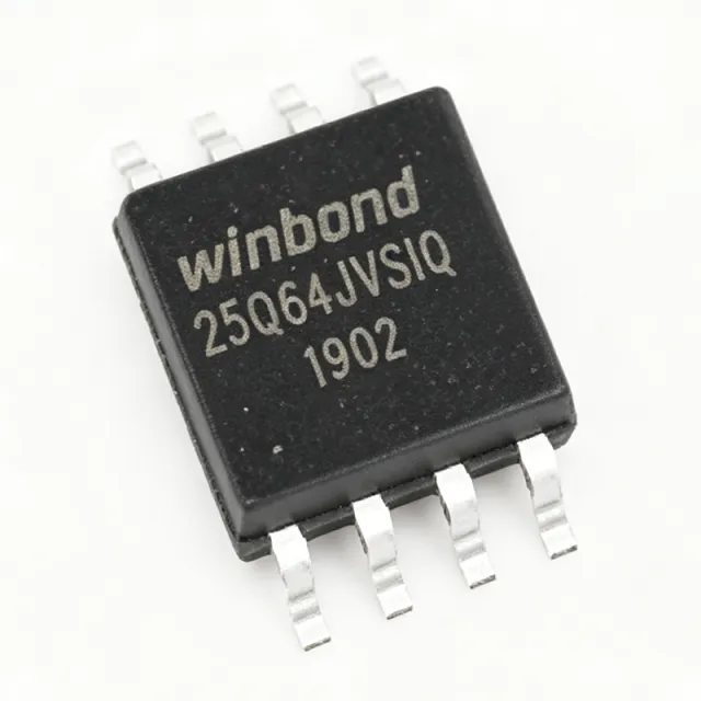
W25Q64JVSSIG - 64Mb SPI Flash 133MHz Industrial | Winbond
W25Q64JVSSIG

W25Q64JVSSIG - 64Mb SPI Flash 133MHz Industrial | Winbond

The Winbond W25Q64JVSSIG is a 64M-bit (8MB) serial NOR flash memory with Dual/Quad SPI and QPI support, operating at 3V to 3.6V and clock speeds up to 133 MHz, housed in an 8-pin SOP (208-mil, SS / SOIC-8) package. The IG suffix denotes the industrial temperature range of -40C to +85C. A serial NOR flash memory is a non-volatile storage IC that stores data in a NOR cell array and communicates over a serial peripheral interface (SPI). Unlike NAND flash, NOR flash offers random access to any address, making it the standard choice for code storage (XIP - execute in place) in embedded systems. It sits within the memory hierarchy: SPI NOR flash -> NOR flash -> flash memory -> semiconductor memory. Key features include Quad SPI with up to 133 MHz clock (equivalent to 532 Mbps transfer), QPI (Quad Peripheral Interface) mode for faster command handling, DTR (Double Transfer Rate) support on JV variants, a 256-byte page program buffer, 4KB sectors, 32KB/64KB blocks, and hardware/software write protection. Advanced security features include individual block lock-down and a 64-bit unique ID, with the G suffix indicating Winbond's industrial-grade flow. The device uses Winbond's proven serial flash architecture with fast erase times and low power consumption, featuring a deep power-down mode that reduces standby current to microamp levels - critical for battery-powered designs. JEDEC SFDP support simplifies second-sourcing against compatible parts. Typical applications include embedded code storage for microcontrollers and DSPs, Wi-Fi/Bluetooth module firmware, BIOS/UEFI storage on industrial PCs, LCD/OLED display drivers, and IoT sensor nodes. Design tip: enable the QE (Quad Enable) bit in the status register for quad operation, and verify JEDEC SFDP compatibility when second-sourcing against GigaDevice GD25Q64 parts. This page synthesizes distributor pricing, drop-in alternatives, and practical design notes not found in the manufacturer datasheet. Pricing references are as of 2026-09-06.

USD $0,22 Auf Lager
W25X40CLZPIG - 4Mbit SPI NOR Flash, 104MHz, 8-WSON | Winbond
W25X40CLZPIG

W25X40CLZPIG - 4Mbit SPI NOR Flash, 104MHz, 8-WSON | Winbond

The Winbond W25X40CLZPIG is a 4 Mbit SPI NOR flash memory IC operating at up to 104 MHz clock frequency in an 8-pin WSON (6x5 mm) package with exposed pad. It provides 512K x 8 organization with uniform 4 KB sectors and supports standard SPI, Dual SPI, and Quad SPI instruction sets. The device operates from 2.5V to 3.3V supply, delivering low-power, high-throughput non-volatile storage for embedded systems. A NOR flash memory is a type of non-volatile storage that retains data without power and supports execute-in-place (XIP) operation, where the CPU can read instructions directly from the flash instead of copying them to RAM first. Within the broader semiconductor taxonomy, NOR flash belongs to the non-volatile memory family (alongside NAND flash and EEPROM) and is widely used for code storage and firmware in microcontrollers, IoT devices, and consumer electronics where random read latency matters more than write density. Key features include 104 MHz maximum clock rate, 4 KB uniform sector granularity, page program up to 256 bytes per command, sector erase time of 40 ms typical, and JEDEC-standard manufacturer/device ID reading. The W25X40CLZPIG also offers hardware and software write protection via the /WP pin and STATUS register, plus an internal 3-byte unique ID for security. The architecture uses a single-transistor NOR cell array with hot-electron-injection programming and Fowler-Nordheim tunneling erase, controlled by an embedded state machine. Winbond's proprietary SpiFlash command set allows bit-shifted SPI mode enabling Dual I/O (DIO) for doubled throughput or Quad I/O (QIO) for quadrupled throughput without changing pin count. Typical applications include firmware storage for IoT sensors, boot code in industrial controllers, configuration storage in smart-home devices, data logging in metering equipment, and parameter storage in wearable devices. Compared with NAND flash, NOR flash offers faster random reads at the cost of lower density per dollar. When designing with this part, place a 0.1 uF decoupling capacitor close to the VCC pin and provide a clean GND return path to the exposed pad, which also acts as the chip's main thermal path. Avoid long SPI traces - keep traces under 50 mm or use a series resistor to dampen ringing on the SCK line. This page synthesizes distributor pricing, drop-in alternatives, and practical design notes not found in the manufacturer datasheet.

USD $0,58 Auf Lager
W25X40CLZPIG-TR - 4Mbit SPI NOR Flash 104MHz 8-WSON | Winbond
W25X40CLZPIG-TR

W25X40CLZPIG-TR - 4Mbit SPI NOR Flash 104MHz 8-WSON | Winbond

The Winbond W25X40CLZPIG-TR is a 4 Mbit (512 Kbit x 8) serial NOR Flash memory device with SPI and Dual-SPI bus interface, operating at up to 104 MHz clock frequency in an 8-pin WSON (6x5 mm) package with exposed pad. It supports 2.5V/3.3V operating voltage and offers 4 KB uniform sector architecture with hardware and software write protection. A serial NOR flash is a non-volatile memory that stores data persistently and communicates over a low pin-count SPI bus. The W25X40 belongs to the spiFlash family, a category of small-footprint flash memories widely used for boot code, firmware, and configuration storage in embedded systems. Compared to parallel NOR flash, spiFlash devices trade raw bandwidth for fewer pins (4-8 vs. 32+), enabling compact PCB layouts in cost-sensitive designs. Key features of the W25X40CLZPIG-TR include 104 MHz maximum SPI clock, 8 ns access time, page program (up to 256 bytes per command), 4 KB sector erase granularity, 32 KB and 64 KB block erase options, hardware write-protect pin, software write-protection via status register, JEDEC standard manufacturer and device ID read, and an operating temperature range of -40C to +85C. The 8-WSON package with exposed pad provides a small footprint (6 mm x 5 mm) and good thermal dissipation. The W25X40CLZPIG-TR uses a single 2.5V to 3.3V supply and is fully static, requiring no external clock. Internally the device implements a state-machine-based command interpreter that decodes instruction opcodes (Read, Page Program, Sector/Block Erase, Read Status, etc.) issued over the SPI bus. Dual-SPI mode doubles throughput by using two data lines for read operations, useful for XIP (execute-in-place) boot from flash. Typical applications include router and home gateway firmware storage, set-top box boot loaders, IoT device firmware, industrial sensor data logging, and Bluetooth/Wi-Fi module configuration storage. It is frequently paired with low-cost MCUs that lack internal flash of sufficient capacity. When designing with this part, place a 0.1 uF decoupling capacitor as close as possible to the VCC pin and connect the exposed pad to a solid ground plane for thermal relief. The /WP and /HOLD pins should be tied to VCC via pull-ups if unused, to prevent accidental write protection or bus stalls during firmware updates. This page consolidates distributor pricing, same-brand and cross-brand drop-in alternatives, and practical design notes beyond what the Winbond datasheet alone provides, helping engineers select and source the right SPI flash for cost-sensitive embedded designs.

USD $0,49 Auf Lager
W29EE011P-90 - 1Mb 5V Parallel Flash, 90ns, 32-PLCC | Winbond
W29EE011P-90

W29EE011P-90 - 1Mb 5V Parallel Flash, 90ns, 32-PLCC | Winbond

The Winbond W29EE011P-90 is a 1-megabit (128K x 8) CMOS parallel flash memory with 90 ns access time, organized as 128K bytes and packaged in a 32-pin PLCC. It operates from a single 5V supply and supports in-system program and erase operations without requiring a 12V VPP. A flash memory is a non-volatile storage technology that retains data when power is removed and supports electrical erase and program cycles in circuit. The W29EE011P-90 sits within the memory IC hierarchy as a parallel NOR flash, distinct from serial SPI flash (fewer pins, lower pin count) and NAND flash (higher density, page/block oriented). Parallel NOR flash is the legacy choice for code storage in 8-bit and 16-bit microcontrollers, EPROM replacement, and firmware boot ROMs where byte-level random access and simple bus interface are required. The W29EE011P-90 features 90 ns maximum access time, sector/chip erase capability, and CMOS low-power operation. It is designed as a drop-in replacement for legacy 5V EPROMs and standard 1-Mbit flash devices. The 32-PLCC package provides a JEDEC-standard pinout compatible with the industry 1-Mbit parallel flash footprint, simplifying board-level migration from older AMD/Atmel/ST 28F001 or 29EE011 sockets. Typical applications include embedded firmware storage for industrial controllers, legacy 8051/68HC11/MCS-96 system boot memory, BIOS and firmware update banks, point-of-sale terminals, and industrial PLC code storage. The 90 ns access time supports microcontrollers running at up to approximately 8 MHz without wait states. When designing with this part, note that the 32-PLCC package requires a PLCC socket or careful reflow profile for surface-mount assembly. Verify the device's command set (byte programming, sector erase, chip erase) against your firmware's flash algorithm before substitution. The part is suitable for 5V-only systems; it does not support 3.3V operation.

USD $0,38 Auf Lager
W29N01HVBINF - 1Gbit 3V SLC NAND Flash 63-VFBGA | Winbond
W29N01HVBINF

W29N01HVBINF - 1Gbit 3V SLC NAND Flash 63-VFBGA | Winbond

The Winbond W29N01HVBINF is a 1 Gbit (128 M x 8) Single-Level Cell (SLC) NAND Flash memory organized as 1024 blocks of 64 KB each, supplied in a compact 63-ball VFBGA (9 mm x 11 mm) package. It operates from a single 3.0 V power supply (2.7 V to 3.6 V) and provides asynchronous x8 parallel I/O with typical page-read access of 25 ns, making it well suited for embedded code and data storage where reliability and endurance matter more than raw throughput. NAND Flash is a non-volatile memory technology that stores bits as charge on a floating-gate MOSFET cell. SLC NAND stores one bit per cell, which delivers 10x the endurance and 10x the data retention of MLC or TLC NAND at the cost of lower density per die. Within the storage taxonomy, NAND Flash sits below NOR Flash for code execution and below DRAM for volatile working memory, but above raw EEPROM in density-per-area. The 1 Gbit SLC class targets boot-loaders, firmware images, and transaction logs in set-top boot boxes, industrial HMIs, and IoT gateways where predictable write performance and 100 K P/E cycles are non-negotiable. Key features of the W29N01HVBINF include ONFI 1.0 compatibility, an internal 4-bit ECC engine that corrects up to 4 bit errors per 528-byte sector, a 2112-byte page size (2048 data + 64 spare), a block erase time of 2 ms typical, and a page program time of 250 us typical. The chip supports two ground pins for noise isolation, a hardware write protect pin, and a HOLD# pin that allows the host to pause operations mid-bus cycle without de-asserting chip enable. Architecturally the W29N01HVBINF uses a charge-trap-compatible floating-gate cell array with on-chip charge pumps generating the high voltages required for program and erase operations, so the host only supplies 3.3 V. The integrated ECC reduces host CPU load and corrects soft errors that occur naturally during the operational lifetime of the NAND array, which is critical because raw NAND bit error rate (RBER) climbs as the part approaches its end-of-life P/E count. Typical applications include set-top box firmware storage, industrial IoT gateways, eMMC boot, point-of-sale terminals, and automotive infotainment reference data. Designers choose this Winbond SLC when they need ONFI-compliant timing for an existing host controller, or when they need a second-source drop-in part for a Samsung or Toshiba SLC die. A key design consideration is that the W29N01HVBINF requires 4-bit ECC for every read of 528 bytes; disabling ECC on the host side will reduce endurance and reliability significantly, and is not recommended by the manufacturer. Always sequence WP#, HOLD#, and CE# transitions per the AC timing diagram in section 4 of the manufacturer datasheet. This page synthesizes distributor pricing, ONFI-compatible drop-in equivalents, and practical hardware-design notes not found in the manufacturer datasheet alone.

USD $1,21 Auf Lager
W29N01HVBINF-TR - 1Gb 3V SLC NAND Flash, 63-VFBGA | Winbond
W29N01HVBINF-TR

W29N01HVBINF-TR - 1Gb 3V SLC NAND Flash, 63-VFBGA | Winbond

The Winbond W29N01HVBINF-TR is a 1 Gbit (128 MB) Single-Level Cell (SLC) NAND Flash memory organized as an 8-bit multiplexed I/O bus and housed in a 63-ball VFBGA (9x11 mm) package. It operates from a 2.7V to 3.6V single supply with a typical 20 ns random-access time and ONFI 1.0 compliance. The device uses a 2048 + 64 byte page architecture and supports the standard NAND command set including program, read, erase, and copy-back operations. A NAND Flash memory is a non-volatile storage technology that retains data without power by storing charge on floating-gate transistors. SLC NAND stores one bit per cell, delivering the highest endurance (typically 100k P/E cycles), fastest write speeds, and longest data retention among NAND types - making it the preferred choice for code storage, boot media, and industrial data logging where MLC/TLC reliability would be inadequate. The W29N-HV family sits in the ONFI 1.0 standard ecosystem (NAND Flash -> non-volatile memory -> memory IC -> semiconductor), allowing seamless software reuse across vendors. Key features include a 1 Gbit density in the smallest standard NAND footprint, hardware WP# (Write Protect) and R/B# (Ready/Busy) status pins, 4-bit ECC requirement per 528 bytes, and an extended operating temperature range suitable for industrial applications. The device uses a 3V VCC for both the core and I/O, simplifying power-tree design by removing the 1.8V requirement common to higher-density parts. Typical applications include embedded Linux/Android boot storage on routers, set-top boxes, and IoT gateways; firmware and asset-log retention in industrial control and metering equipment; data logging in automotive infotainment and telematics modules; and code shadowing from NOR/ROM to faster NAND in consumer electronics. The 63-VFBGA package is footprint-compatible with the wider Winbond W29N family, enabling PCB reuse across 1 Gb to higher densities. When designing with this part, ensure the host controller or SoC implements the ONFI 1.0 software driver and a BCH or Hamming ECC engine capable of 4-bit correction per 528-byte sector. For long-term reliability, apply wear-leveling at the file-system (e.g., UBI/YAFFS/JFFS2) or FTL layer, because raw NAND blocks wear out at the rated P/E cycle count. This page synthesizes Winbond datasheet specifications, current distributor pricing, drop-in alternatives, and practical design notes not consolidated on any single manufacturer or distributor page. The W29N01HVBINF-TR is halogen-free and RoHS compliant per the Winbond product page. The 'TR' suffix denotes Tape and Reel packaging suitable for high-volume SMT assembly.

USD $1,62 Auf Lager
W5100 - 10/100 Ethernet Controller with TCP/IP | WIZnet
W5100

W5100 - 10/100 Ethernet Controller with TCP/IP | WIZnet

WIZnet W5100 is a single-chip Internet-enabled 10/100 Ethernet controller for embedded systems, integrating TCP/IP, MAC, and PHY functions in an 80-LQFP 10 x 10 mm package. The controller supports 10/100 Base-T/TX Ethernet connectivity through an SPI interface, reducing the need for a host processor to manage low-level network stacks. An Ethernet controller is an interface IC that connects an embedded processor to a physical network. In the W5100, the MAC, TCP/IP hardware, and 10/100 PHY are integrated into one device, allowing the host MCU or CPU to communicate through SPI while the controller handles Ethernet framing and protocol processing. The verified distributor listing identifies W5100 as a 10/100 Base-T/TX Ethernet controller with an SPI interface and an 80-LQFP package. The manufacturer datasheet describes the device as a full-featured, single-chip Internet-enabled controller designed for embedded applications where integration stability, performance, area, and system cost control are important. W5100 is suited to industrial embedded equipment, control systems, instrumentation, building automation, and other Ethernet-connected products. Its integrated architecture can simplify hardware design by combining the Ethernet MAC and PHY with hardware-assisted TCP/IP functions, while the SPI host interface keeps the external processor interface compact. The 10/100 Ethernet capability makes W5100 appropriate for legacy and cost-sensitive networks operating at 10 or 100 Mbit/s. The exact PHY, electrical, timing, temperature, memory, and SPI operating details should be confirmed directly in the manufacturer datasheet before final schematic, layout, and qualification decisions. The W5100 is not a power semiconductor, so a safe operating area is not applicable. Proper implementation requires attention to Ethernet magnetics, RJ45 integration, PCB signal integrity, power sequencing, decoupling, and the exact pin assignments shown in the official documentation. This page consolidates the verified product description, distributor package information, datasheet links, and engineering-oriented application guidance.

Angebot Auf Lager
W5500 - Hardwired TCP/IP Ethernet Controller SPI | WIZnet
W5500

W5500 - Hardwired TCP/IP Ethernet Controller SPI | WIZnet

The WIZnet W5500 is a hardwired TCP/IP embedded Ethernet controller that integrates the TCP/IP stack, 10/100 Ethernet MAC, and PHY in a single chip, communicating to a host MCU over an SPI bus at up to 80 MHz. It provides 8 simultaneous sockets with 32 KB of internal TX/RX buffer memory and is housed in a 48-pin LQFP (7x7 mm) package. An Ethernet controller (also called a network controller or NIC controller) is a semiconductor device that offloads the low-level networking functions - framing, MAC addressing, PHY transceiver signaling, and protocol handling - from the host microcontroller. Hardwired TCP/IP controllers go further by implementing the TCP, UDP, IPv4, ICMP, PPPoE, ARP, and IGMP protocols in dedicated silicon rather than firmware. Within the broader taxonomy, the W5500 sits at: Ethernet controller -> network controller -> communication IC -> semiconductor. Compared to a microcontroller running an LWIP software stack, a hardwired controller delivers deterministic latency, low MCU overhead, and a smaller code footprint, but lacks the flexibility of full-protocol software stacks. Key features include 10/100 Base-TX auto-negotiation, full/half-duplex operation, 8 independent socket buffers, a wake-on-LAN (WoL) pin for remote wake scenarios, and integrated 802.3az energy-efficient Ethernet support. The SPI interface runs from 0 to 80 MHz in variable-length mode and supports Mode 0 / Mode 3, allowing direct connection to most ARM Cortex-M, ESP32, AVR, and PIC hosts without glue logic. The W5500's architecture is built around a hardwired protocol engine and dedicated socket memory blocks. Each of the 8 sockets has a Tx buffer and Rx buffer routed through an internal DMA-like engine, so the host MCU does not have to manage TCP state machines. The embedded PHY supports HP Auto-MDIX, eliminating the need for crossover cables. Compared to the legacy W5100 (80-pin), the W5500 reduces pin count to 48 and adds SPI efficiency improvements, while W5100S retains the 80-pin footprint for drop-in W5100 upgrades. Typical applications include IoT sensor nodes, industrial Ethernet PLCs, smart-home gateways, IP-camera control planes, and Arduino/MCU Ethernet shields. The 32 KB buffer is sufficient for most MQTT/CoAP/HTTP payloads without external memory, and the SPI bus allows the part to be wired directly to microcontrollers that lack integrated Ethernet MAC/PHY. Design consideration: because the W5500 integrates the PHY, the board must route the MDI differential signals as a 100-ohm differential pair and provide a 1:1 center-tap magnetics module. Decouple both 3.3 V analog and digital rails at the chip pins with 0.1 uF and 10 uF ceramics; share ground with the host MCU through a single stitch. This page synthesizes distributor pricing, same-family drop-in alternatives, and practical hardware-design notes not consolidated in the manufacturer datasheet.

USD $1,78 Auf Lager
W55RP20 - RP2040+W5500 Ethernet SiP MCU | WIZnet
W55RP20

W55RP20 - RP2040+W5500 Ethernet SiP MCU | WIZnet

The WIZnet W55RP20 is a System-in-Package (SiP) ioMCU that integrates the Raspberry Pi RP2040 dual-core Arm Cortex-M0+ microcontroller running at 133 MHz with the W5500 hardware TCP/IP Ethernet controller, in a 68-pin VFQFN exposed-pad package. It combines 2 MByte of on-chip flash memory and 264 kB of on-chip SRAM organized in six independent banks with a full hardwired TCP/IP stack and a 12-channel DMA controller. A System-in-Package device stacks or side-by-side mounts two dies within a single molded package, so the W55RP20 functions electrically as one microcontroller with built-in Ethernet, eliminating the two-chip RP2040-plus-W5500 solution that previously required separate routing, crystals, and power domains. In the product hierarchy it sits as: ioMCU -> communications controller microcontroller -> Ethernet microcontroller -> IoT connectivity IC. Key features include the dual Cortex-M0+ cores at 133 MHz, 2 MB flash for code storage, 264 kB SRAM in six independent banks, and the W5500 subsystem with a hardwired TCP/IP stack supporting 8 hardware sockets, which offloads protocol processing entirely from the CPU. A 12-channel DMA controller supports memory-to-peripheral, peripheral-to-memory, and memory-to-memory transfers, each channel with its own control and status registers, letting the processor switch to other tasks or low-power states during large data transfers. The W5500 die provides a hardware TCP/IP stack implementing MAC and PHY functionality for 10/100 Mbps Ethernet, so networking is deterministic and does not consume MCU cycles for protocol handling. This architecture suits applications where wire-speed throughput and low jitter matter more than a large software network stack. Typical applications include industrial IoT gateways, networked sensor nodes, smart-building controllers, and Ethernet-enabled embedded systems where developers want Raspberry Pi Pico-class processing plus native wired networking in one chip. Design consideration: as a SiP, thermal dissipation is combined from both dies; verify total power budget and provide adequate ground-plane copper under the exposed pad for heat spreading and signal return. This page synthesizes distributor pricing, availability, evaluation-board references, and practical design notes not consolidated in the manufacturer datasheet.

USD $2,45 Auf Lager