CI de interfaz
Subcategorías
Productos (1019)

1734-4IOL - POINT I/O 4-Channel IO-Link Master Module
The Allen-Bradley 1734-4IOL is a POINT I/O 4-channel IO-Link master module designed to bridge intelligent IO-Link sensors and actuators to an EtherNet/IP-based Logix control system. As a Series B POINT I/O module, the 1734-4IOL installs on a standard 1734 terminal base and connects upstream through a 1734-AENT or 1734-AENTR Ethernet adapter, exposing four independent IO-Link ports that conform to the IO-Link v1.0/1.1 specification. Each channel supports standard digital input, standard digital output, IO-Link, Fallback, or Disabled modes, allowing a mix of conventional discrete I/O and full bidirectional IO-Link communication on the same module. An IO-Link master is a fieldbus gateway that provides a point-to-point digital communication channel between a controller and a single IO-Link device (sensor or actuator), serving as the IO-Link backbone in the industrial sensor-to-cloud hierarchy (IO-Link device -> IO-Link master -> fieldbus/industrial Ethernet -> PLC/DCS). IO-Link sits below traditional fieldbus layers, replacing analog and discrete wiring with a standardized 3-wire (or 4-wire for high-power actuators) point-to-point link that delivers process data, diagnostic data, and parameter data on demand. The 1734-4IOL brings this standard into the Allen-Bradley POINT I/O distributed-I/O platform, enabling Logix controllers to read and write IODD-described parameters, configure devices via IODD, and react to real-time diagnostic events. Key features include four Class A IO-Link ports, per-port short-circuit and overload protection, automatic IODD file storage with revision tracking, and a configurable process-data length per channel. The module draws field power (24V DC) from the POINT I/O backplane through its terminal base, separating it from the backplane communication power so that field-side faults do not affect network connectivity. Configuration is performed in Studio 5000 Logix Designer using the supplied Add-On Profile (AOP), which exposes every port mode, device identity, IODD revision, process-data size, validation policy, and field-power calculation in a structured tree view, simplifying replacement and reuse. Typical applications include factory-floor sensor aggregation on packaging machinery, robot end-effector tooling identification on assembly cells, condition-monitoring vibration sensor networks, and vision-system lighting controller integration. The compact 12.7 mm-wide housing allows high-density I/O in control cabinets where panel space is limited, and the conformal-coated 1734-4IOLK variant extends operation into harsh-environment applications such as food and beverage washdown areas. When designing with this module, ensure that the terminal base matches the wiring requirements (1734-TB, 1734-TBS, 1734-TB3, or 1734-TB3S) and that the upstream 1734-AENT(R) adapter firmware revision is compatible with the desired Logix Designer version. Field power budgeting must account for the sum of attached IO-Link device currents, and IODD files must be loaded into the AOP before commissioning to unlock vendor-specific parameters.

74LV4053D,118 - Triple SPDT Analog Switch, 2:1 MUX, SO-16 | Nexperia
The Nexperia 74LV4053D,118 is a triple single-pole double-throw (SPDT) analog switch implemented in low-voltage CMOS logic, housed in a 16-pin small-outline (SO-16 / SOT109) surface-mount package. The IC operates from a single 1.0 V to 6.0 V supply rail, supports 2:1 multiplexing/demultiplexing of analog or digital signals, and provides a typical on-resistance of 105 ohm (225 ohm maximum) per channel. Each switch section features an independent digital select input (Sn), two bidirectional I/O pins (nY0, nY1), and a common bidirectional I/O pin (nZ), with all channels sharing a single enable input. An analog switch IC (also called a CMOS transmission gate or bilateral switch) is a solid-state device that uses MOSFET pairs to route analog or digital signals between multiple nodes without mechanical contacts. Analog switches sit at the boundary between the analog signal chain and the digital control logic, performing the same role that mechanical relays performed historically, but with far higher speed, lower power, no contact bounce, and essentially infinite mechanical life. The 74LV4053 belongs to the broader category of multiplexer/demultiplexer (MUX/DEMUX) ICs, which themselves fall under the interface ICs hierarchy within the integrated-circuit taxonomy. Key differentiating features include very low quiescent current (a few microamps at 25 °C), fast switching with typical turn-on (tON) of 190 ns and turn-off (tOFF) of 125 ns at 3 V, 5 ohm on-resistance matching between channels (Delta-RON), and 50 dB off-isolation (VISO) at typical audio frequencies. The device is pin- and function-compatible with the higher-voltage 74HC4053 and 74HCT4053 families, allowing direct substitution in existing footprints when a lower-voltage rail is acceptable. Integrated logic-level translation also makes it suitable for interfacing 5 V controllers with 1.8 V or 3.3 V peripherals. Architecturally, the 74LV4053D uses N-channel and P-channel MOSFET pairs in a transmission-gate topology for each of the three switches; the CMOS process delivers bidirectional signal handling from rail to rail, low charge injection, and high input impedance for both analog and digital signals. Because all switches share a common substrate, designers should observe standard ESD handling precautions and avoid signal voltages that exceed VDD7. Typical applications include audio signal routing in portable consumer devices, multiplexing sensor outputs to a microcontroller ADC, video or composite signal switching, communication line routing, and general-purpose signal-path selection in industrial and automotive subsystems. The wide 1.0 V to 6.0 V supply range makes the part equally comfortable in coin-cell powered IoT nodes and 5 V legacy systems. When designing with this device, ensure that the analog signal swing remains within the VDD and GND rails to prevent latch-up of the internal transmission-gate MOSFETs. Add 100 nF ceramic bypass capacitors adjacent to VDD and GND, and route digital select lines away from sensitive analog traces to preserve the 50 dB off-isolation figure. This page consolidates distributor pricing, verified drop-in alternatives, and practical design notes that are not assembled in the manufacturer short datasheet, providing engineers with a single source for procurement and design decisions.

74LVC1G3157GW - 10Ω SPDT Analog Switch | Nexperia 6-TSSOP
The Nexperia 74LVC1G3157GW is a single-pole double-throw (SPDT) analog switch housed in a 6-pin TSSOP (SOT363) package, featuring 10Ω typical ON resistance and a 1.65V to 5.5V supply range. This device provides a 2:1 analog multiplexer/demultiplexer function with break-before-make switching and 32 mA switch current capability. According to the Nexperia datasheet, the part operates from 1.65V to 5.5V VCC with control inputs tolerant of 3.3V and 5V drive levels, enabling mixed-voltage signal routing in modern low-voltage systems. An analog switch (also called a bilateral switch or pass gate) is a semiconductor device that uses MOSFET transistors to route analog or digital signals between multiple paths under digital control. The 74LVC1G3157 sits in the broader hierarchy of: analog switch → multiplexer/demultiplexer → interface IC → integrated circuit → semiconductor. Single-pole double-throw switches like this are the simplest multiplexers and form the foundation of signal routing in mixed-signal systems, providing isolation between channels, level shifting between voltage domains, and dynamic signal path selection. Key features include very low ON resistance of 7.5Ω typical at VCC=2.7V, 6.5Ω typical at VCC=3.3V, and 6Ω typical at VCC=5V, with ESD protection exceeding 2000V HBM per JESD22-A114F. The device offers high noise immunity CMOS construction, TTL interface compatibility at 3.3V, and CMOS low power consumption. Latch-up performance meets JESD 78 Class I requirements, ensuring robust operation in demanding environments. The 74LVC1G3157 employs a parallel MOSFET topology where the select input (S) drives complementary gate signals to connect the common terminal (Z) to either Y0 or Y1. This architecture delivers excellent signal fidelity across the full analog input range (0V to VCC) with minimal distortion. The break-before-make switching eliminates momentary shorts between Y0 and Y1 during transitions, protecting source and downstream circuitry. Typical applications include signal routing in portable consumer devices, audio source switching in headsets, USB signal multiplexing, GPIO expansion in microcontrollers, and voltage domain translation between 1.8V, 3.3V, and 5V systems. The wide supply range and TTL-compatible inputs make this part ideal for bridging legacy 5V peripherals with modern 1.8V processors. When designing with this device, ensure VCC is well-decoupled with a 100nF ceramic capacitor placed close to the supply pin. The analog signal range is rail-to-rail (0V to VCC), but exceeding VCC on any signal pin will forward-bias the ESD protection diodes. For hot-plug applications, add series resistance to limit inrush current.
88SE9235 - 4-Port SATA 6Gbps PCIe 2.0 x2 Controller | Marvell
The Marvell 88SE9235 is a four-port SATA 6 Gbps host bus adapter controller with a two-lane PCIe 2.0 host interface, housed in a 76-terminal HVQCCN (QFN) package and fabricated on a 55 nm CMOS process. A SATA host controller (also called an HBA controller or SATA I/O controller) is a storage interface IC that connects SATA devices such as HDDs, SSDs, and optical drives to a host system over the PCI Express bus. Within the system hierarchy, it sits between the PCIe root complex and the physical SATA ports, handling the Serial ATA protocol stack, command processing, and PHY-layer serialization. The 88SE9235 belongs to Marvell's 88SE92xx family of PCIe-to-SATA controllers. Key features include four independent SATA ports supporting both 3 Gbps (SATA II) and 6 Gbps (SATA III) link speeds, compliance with the Serial ATA Revision 3.1 specification from the Serial ATA International Organization, and a PCIe 2.0 interface with up to two lanes delivering up to 2 GB/s of aggregate bandwidth toward the host. This makes the device well suited for designs that must connect more SATA ports than a chipset natively provides. Technically, the integrated PHY, link, and transport layers reduce external component count, while the 55 nm CMOS process keeps power consumption appropriate for embedded and consumer platforms. Marvell positions the 88SE9235 both for embedded platform applications and for HBA vendors who develop their own RAID software or rely on in-box OS drivers, simplifying driver bring-up across Windows and Linux environments. Typical applications include home NAS and media servers, DVR/NVR video-recording platforms, set-top boxes, and add-in SATA host bus adapter cards requiring four 6 Gbps ports on a single PCIe x2 slot. When designing with this device, verify that the PCIe 2.0 x2 link bandwidth (up to 2 GB/s raw) is not oversubscribed when all four SATA ports operate at 6 Gbps concurrently; host bandwidth planning is essential for multi-drive RAID workloads. This page synthesizes distributor pricing channels, family drop-in alternatives, and practical design notes not found in the manufacturer datasheet alone.

89H24NT24G2ZCHLGI - 24-Lane/24-Port PCIe Gen2 Switch | Renesas
The Renesas 89H24NT24G2ZCHLGI is a 24-lane, 24-port PCI Express Gen2 system interconnect switch housed in a 324-pin FCBGA (19x19 mm) package, originally developed by Integrated Device Technology (IDT, now part of Renesas). It delivers full line-rate, non-blocking throughput on all 24 ports simultaneously, providing deterministic switching across multiple traffic flows regardless of load. The device is part of the 89HPES24NT24G2 family and targets high-performance server, storage, and embedded switching fabrics. A PCIe Gen2 system interconnect switch is a semiconductor device that expands the number of PCIe endpoints a root complex can service by routing Transaction Layer Packets (TLPs) between upstream ports and multiple downstream ports. Switches sit hierarchically below root complexes and endpoints in the PCIe topology and are essential for fan-out in dense compute and storage systems. Each Gen2 lane runs at 5 GT/s, doubling the bandwidth of Gen1 (2.5 GT/s) and enabling higher per-port throughput while preserving backward compatibility with Gen1 endpoints. Key features of the 89H24NT24G2ZCHLGI include support for PCI Express Gen2 (5.0 GT/s) on all 24 lanes, 24 configurable ports, non-blocking cut-through architecture, and integrated clocking with spread-spectrum support. The device supports maximum payload sizes up to 4096 bytes (MPS), Extended Configuration Space access, and provides per-port flow control. Power management is implemented through PCI-PM 1.2 compliant link states and proprietary low-power modes that gate unused ports, reducing idle consumption in dense designs. The switch fabric uses a multi-stage shared-memory architecture that preserves packet ordering and supports peer-to-peer routing between any two downstream ports without host intervention. This enables direct memory transfers in heterogeneous compute topologies (e.g., GPU-to-storage, NVMe-to-CPU) and minimizes root-port bottlenecking. The on-chip SerDes supports Gen2 electrical signaling with adaptive equalization and de-emphasis for compliance with PCI-SIG CEM specifications across standard channel reaches up to approximately 12 inches of FR4. Typical applications include NVMe storage fabrics in hyperscale servers, multi-host disaggregated storage platforms, GPU expansion chassis, embedded industrial backplanes, and PCIe-over-cable fan-out systems. The 324-FCBGA package supports high-density PCB designs with controlled-impedance routing for the 24 SerDes lanes. End-of-life (Obsolete) status affects long-term availability but the part remains supported by Renesas for embedded and legacy server customers. Design considerations: maintain 85-ohm differential impedance on all 24 SerDes lanes, provide matched-length routing within 5 mils to preserve Gen2 eye margins, and ensure robust reference clock distribution with the on-chip PLL bypass option. The device requires multiple voltage rails (core, SerDes, I/O); refer to the manufacturer datasheet for decoupling topology. This page synthesizes distributor pricing, drop-in alternatives, and engineering design notes beyond the manufacturer datasheet.

AD1938YSTZ - 4ADC/8DAC 192kHz 24-Bit Audio CODEC LQFP-48 | ADI
The Analog Devices AD1938YSTZ is a high-performance single-chip audio codec that integrates 4 analog-to-digital converters (ADCs) with differential inputs and 8 digital-to-analog converters (DACs) with single-ended outputs, housed in a 48-lead LQFP (7x7 mm) package. The device supports sample rates from 8 kHz to 192 kHz at 24-bit resolution, operates from a single 3.3 V supply (with 5 V tolerant logic inputs), and is controlled via an SPI port. An audio CODEC (coder-decoder) is a mixed-signal IC that converts analog audio signals to digital and digital audio signals back to analog, sitting at the intersection of the signal chain between analog transducers (microphones, amplifiers, speakers) and the digital signal processor (DSP) or microcontroller. The AD1938 belongs to the broader category of audio interface ICs, specifically the multi-channel CODEC family, and sits within Analog Devices' precision signal-chain portfolio for professional and prosumer audio. Key features of the AD1938 include 107 dB DAC dynamic range and SNR, 107 dB ADC dynamic range, -94 dB THD+N, a low-EMI design with on-chip PLL for flexible clock generation, software-controllable clickless mute, a logarithmic volume control with autoramp function, and master/slave modes supporting up to 16 devices on a single TDM bus. The codec also integrates TDM, I2S, left-justified, and right-justified serial audio interface modes. The AD1938 employs Analog Devices' patented multibit sigma-delta (Σ-Δ) modulator architecture with a switched-capacitor DAC topology. The integrated PLL allows direct MCLK input up to 27 MHz or generation of internal clocks from a 256 x Fs reference, simplifying board-level clock trees in multi-codec systems. The differential ADC input paths maximize common-mode rejection for balanced microphone or line-level capture. Typical applications include automotive head units and infotainment systems, AV receivers, multichannel mixing consoles, musical instrument amplifiers, effects processors, and broadcast audio equipment. The single 3.3 V supply and 5 V tolerant digital inputs simplify integration into mixed-voltage systems alongside host DSPs or microcontrollers. When designing with the AD1938, ensure adequate decoupling on both AVDD and DVDD rails (typically 10 uF bulk plus 0.1 uF ceramic per pin) and place the master-clock reference within 50 ppm tolerance to avoid PLL jitter. For TDM cascading above 8 channels, the AD1938 can serve as a master driving up to 15 additional slave codecs on a shared data line. This page synthesizes distributor pricing, drop-in same-package alternatives, SPI register notes, and PCB-layout guidance not found in the manufacturer datasheet, providing a 360-degree engineering reference for sourcing the AD1938YSTZ.

AD5142WBCPZ10-RL7 - 10kΩ Dual 256-Tap SPI NVM DigiPot | ADI
The Analog Devices AD5142WBCPZ10-RL7 is a dual-channel, 256-position, nonvolatile (NVM) digital potentiometer with a nominal end-to-end resistance of 10 kΩ, SPI digital interface, and ±8% guaranteed resistor tolerance, housed in a 16-lead LFCSP (3 mm × 3 mm) package with an exposed pad. A digital potentiometer (DigiPot) is a solid-state variable resistor whose wiper position is set by a digital command rather than by mechanical movement. In the system hierarchy, DigiPots sit between mechanical potentiometers/trimmers and analog signal-conditioning chains (gain, offset, bias), functioning as programmable resistors used for calibration, trim, and adaptive control. Because the AD5142 stores the wiper position in onboard EEPROM, the part retains its setting through power cycles, eliminating the need for software re-initialization after every reset and enabling true plug-and-play calibration in factory-trimmed modules. Key features include a 10 kΩ nominal resistance, 256 tap points per channel (resolution ≈ 39 Ω per LSB), SPI-compatible serial interface up to 50 MHz, ±8% end-to-end resistance tolerance, ±6 mA current handling on the A, B, and W terminals, and AEC-Q100 Grade 1 automotive qualification (suffix "W"). The integrated nonvolatile memory supports up to 50,000 write cycles per EEPROM cell, suiting production-line calibration and field-reconfigurable systems. Internally, the AD5142 uses a chain of 256 polysilicon resistors with CMOS transmission-gate switches steered by an EEPROM-backed shift register. The SPI interface exposes a 16-bit command word (3 address + 8 data + control bits), allowing readback of both the volatile RDAC register and the nonvolatile EEPROM image. The "WB" prefix denotes the wide-temperature automotive grade operating from -40 °C to +125 °C. Typical applications include automotive infotainment volume/tone control, programmable gain amplifiers, sensor calibration in ECU modules, programmable voltage references, and instrumentation gain trim. Because the part offers matched dual channels in a tiny 3×3 mm LFCSP, designers can replace two mechanical trimmers with a single I²C-less SPI device, saving board area and enabling fully automated end-of-line calibration. When designing with this device, decouple VDD/VSS with a 0.1 µF ceramic capacitor placed within 2 mm of the supply pin and use a 4-layer PCB with a continuous ground plane tied to the exposed pad to keep thermal resistance low. Account for wiper resistance (~50–100 Ω typical) when computing total end-to-end resistance at low tap counts, and verify that downstream load impedances stay above 1 kΩ to prevent distortion. This page synthesizes current distributor pricing (DigiKey, Mouser, Octopart), pin-compatible ADI drop-in alternatives, and practical PCB/thermal design notes not collected in the manufacturer datasheet alone.

AD5270BCPZ-100-RL7 - 100kΩ 1024-Tap SPI Digital Rheostat | ADI
The Analog Devices AD5270BCPZ-100-RL7 is a single-channel, 1024-position digital rheostat (digitally controlled variable resistor) with 100 kΩ nominal end-to-end resistance, housed in a 10-pin LFCSP-WD (3x3 mm) exposed-pad package. It features SPI serial interface control, ±1% end-to-end resistor tolerance error, 50-TP nonvolatile memory (NVM) for wiper position retention, and operates from a 2.7 V to 5.5 V single supply. What is a digital potentiometer/rheostat? A digital potentiometer (also called a digital rheostat or digipot) is a solid-state, electronically adjustable resistor implemented as a string of series-connected resistive elements with CMOS switches that tap off at programmable nodes. Compared to mechanical trimmers, digipots offer remote, microcontroller-controlled adjustment, no moving parts, higher reliability, and - in nonvolatile variants like the AD5270 - retention of the wiper position across power cycles without a microcontroller continuously writing the setting. Digital potentiometers occupy a position in the signal-chain taxonomy between passive components (resistors) and active analog ICs (variable-gain amplifiers). Key differentiating features of the AD5270BCPZ-100-RL7 include industry-leading 1% end-to-end resistor tolerance error (vs. the 20-30% typical of competing rheostats), 50-times-programmable (50-TP) NVM that allows wiper settings to be permanently written during calibration, and a low-temperature-coefficient architecture that maintains setting accuracy over -40°C to +125°C operation. The 1024-tap resolution provides ~0.1% per-step adjustment granularity, making fine calibration of analog signal chains possible in firmware. The AD5270 is built around a string of precision thin-film resistors with CMOS wiper switches, achieving low wiper resistance and excellent temperature stability. The 50-TP NVM uses fuse-link elements for permanent setting retention, after which subsequent writes are blocked - this prevents accidental overwrites in production. The exposed-pad package provides a low thermal-resistance path that keeps wiper-resistance drift minimal even under sustained write operations. Typical applications include precision programmable-gain instrumentation amplifiers, LCD display contrast/brightness control, laser-driver bias calibration, mechanical potentiometer and trimmer replacement, programmable voltage references, and audio attenuators. The 50-TP NVM is especially valuable in factory-trimmed industrial systems where calibration data must survive power-down. Design consideration: when replacing a mechanical trimmer with the AD5270, account for the limited wiper current (typically a few mA maximum) - the AD5270 cannot source/sink large currents or be used as a true power rheostat; it is intended for signal-level adjustment where it presents a high impedance to the surrounding circuit. This page synthesizes 2026 distributor stock and lead-time, drop-in compatible alternatives, and practical calibration-circuit design notes not found in the manufacturer datasheet alone.
AD5270BCPZ-20 - 20kΩ 1024-Tap SPI Digital Rheostat | ADI
The Analog Devices AD5270BCPZ-20 is a single-channel, 1024-position digital rheostat with 20 kΩ nominal end-to-end resistance, less than 1% resistor tolerance error, and 50-TP (fifty-time programmable) nonvolatile memory, housed in a 10-lead LFCSP-WD (3 mm × 3 mm) package with an exposed pad. It is interface-compatible via SPI and offers 5 V single-supply operation with a rheostat-mode wiper resistance of approximately 35 Ω to 70 Ω, making it suitable for precision analog adjustment in compact systems. A digital rheostat (also called a digital potentiometer or RDAC) is a solid-state variable resistor whose wiper position is set by a digital command instead of a mechanical knob. Internally it is implemented as a string of resistor segments plus MOS switches that connect the wiper to one of the taps; with 1024 taps, the AD5270 achieves roughly 10-bit resolution and supports fine trimming that would otherwise require a manual trim pot. Unlike mechanical trimmers, the wiper position survives power-down thanks to integrated 50-TP EEPROM, allowing the part to be used in factory-calibrated, set-and-forget designs. Key features include 1024-position resolution, 20 kΩ nominal resistance (with -10 and -100 variants also offered), less than 1% end-to-end resistor tolerance error, 50-TP nonvolatile memory for wiper position retention, a standard SPI serial interface, and single 5 V supply operation. The compact 3 mm × 3 mm LFCSP-10 footprint is drop-in compatible with the AD5271 family member, simplifying PCB reuse across resolutions. The exposed pad provides a low-thermal-resistance path, supporting continuous operation across the -40 °C to +125 °C extended industrial temperature range. The architecture combines a precision thin-film resistor string with CMOS switches and on-chip 50-TP EEPROM. The thin-film process delivers the low temperature coefficient and tight absolute tolerance, while the nonvolatile memory allows the part to remember its wiper position through power cycles without requiring continuous software updates. SPI command words are interpreted on-chip to select one of 1024 wiper positions, with readback capability for verifying the stored setting. Typical applications include programmable gain amplification, precision reference adjustment, laser-diode bias trimming, audio volume control, sensor calibration, and instrumentation scaling. Because the part retains its setting in nonvolatile memory, it is well suited to factory-trimmed designs that must boot up with a calibrated state. When designing with this part, observe the absolute maximum wiper current of ±6 mA, decouple VDD with a 1 μF bypass capacitor close to the pin, and ensure the exposed pad is soldered to a sufficient copper pour for thermal dissipation. The 50-TP memory limit should be considered - designs requiring more than 50 writes over the product lifetime must avoid exceeding this threshold. This page synthesizes distributor pricing, drop-in AD5270/AD5271 family variants, and practical design notes that are not aggregated in the manufacturer datasheet.

AD5292BRUZ-100-RL7 - 1024-Tap 100kΩ SPI Digital Potentiometer | Analog Devices
The Analog Devices AD5292BRUZ-100-RL7 is a single-channel, 1024-position digital potentiometer with 100 kΩ end-to-end resistance, nonvolatile memory (20-TP), and an SPI serial interface, housed in a 14-pin TSSOP package rated for -40°C to +105°C operation. The device features ±1% nominal resistor tolerance in R-Perf mode, ±35 ppm/°C resistance temperature coefficient, and 50 ppm typical resistor differential nonlinearity, making it one of the most precise digital pots in its class. A digital potentiometer (or digipot) is a solid-state variable resistor whose wiper position is set by a digital code rather than mechanical action. In the signal chain hierarchy it sits between passive mechanical potentiometers and active digital-to-analog converters (DACs), offering software-controlled resistance adjustment, nonvolatile state retention, and PCB-mountable miniaturization. Digipots are commonly used to replace mechanical trimmers in volume controls, gain stages, and calibration circuits. Key features of the AD5292 include 1% resistor tolerance in R-Perf mode, an SPI-compatible serial interface operating up to 50 MHz, and 20-times programmable nonvolatile memory that retains wiper position through power cycles. The 50 ppm/°C temperature coefficient and 50 ppm resistor differential nonlinearity (DNL) ensure stable, monotonic resistance steps across the operating range, which is critical for instrumentation applications. The AD5292 uses an array of 1024 thin-film resistors with CMOS switches and a wiper decoder. The thin-film process provides low noise, low temperature coefficient, and excellent long-term stability compared to polysilicon alternatives. The internal charge-pump generates the gate voltage required for the analog switches, allowing the device to operate from a single 9 V to 33 V analog supply while the digital interface is referenced to a separate 2.7 V to 5.5 V logic supply, simplifying interface to low-voltage microcontrollers. Typical applications include programmable gain amplifiers, instrumentation gain trimming, LCD contrast control, audio volume attenuation, and programmable voltage references. The wide supply range and high voltage tolerance make it well-suited for industrial 24 V bus systems and precision measurement equipment where mechanical trimmers are not acceptable. When designing with the AD5292, place 0.1 µF bypass capacitors close to the AVDD and DGND pins. The SDO pin contains an open-drain N-channel FET and requires an external pull-up resistor if used. The wiper resistance (typically 60 Ω) should be included in gain-error calculations for high-precision circuits. This page synthesizes AD5292BRUZ-100-RL7 distributor pricing, SPI-compatible drop-in alternatives, and practical design notes not found in the manufacturer datasheet.

AD5700-1ACPZ - HART FSK Modem IC | Analog Devices
The AD5700-1ACPZ is a single-chip HART FSK half-duplex modem from Analog Devices, designed to comply with the HART physical layer requirements. It integrates all necessary filtering, signal detection, modulation, demodulation, and signal generation functions, requiring few external components. The device operates over a supply voltage range of 2.7V to 5.5V and is available in a 24-lead LFCSP-WQ (4x4 mm) package. It features a maximum supply current of 115 µA, making it ideal for loop-powered applications. The AD5700-1 variant includes an integrated 0.5% precision oscillator, saving board space and external component count. A HART modem is a specialized integrated circuit that enables digital communication over analog 4-20 mA current loops, commonly used in industrial process automation. It modulates and demodulates Frequency Shift Keying (FSK) signals at 1200 Hz and 2200 Hz, allowing digital data to be superimposed on the analog signal without interference. The HART protocol is a hybrid analog/digital standard widely adopted in smart transmitters, actuators, and control systems. The AD5700-1ACPZ belongs to the category of communication ICs, specifically modems, and is a key component in industrial communication systems. Key features include a 0.5% precision oscillator, low power consumption of 115 µA, and compliance with HART physical layer specifications. The device supports both master and slave configurations, making it versatile for various applications. It also includes an internal voltage reference and a carrier detect output, simplifying system design. The operating temperature range is -40°C to +125°C, suitable for harsh industrial environments. Technically, the AD5700-1 uses a digital signal processing architecture to achieve reliable FSK modulation and demodulation. The integrated oscillator eliminates the need for an external crystal, reducing component count and board space. The device also features a UART interface for easy connection to microcontrollers. The LFCSP package provides excellent thermal performance and a compact footprint, ideal for space-constrained designs. Typical applications include smart transmitters, process control systems, field instruments, and HART-based communication interfaces. The low power consumption and integrated oscillator make it particularly suitable for loop-powered devices where power is limited. The device is also used in HART master systems, such as handheld communicators and control room equipment. When designing with the AD5700-1ACPZ, ensure proper decoupling of the power supply and careful layout of the analog front-end to minimize noise. The device requires a few external components, including a coupling capacitor and a protection circuit for the HART signal path. Refer to the datasheet for recommended application circuits and layout guidelines.
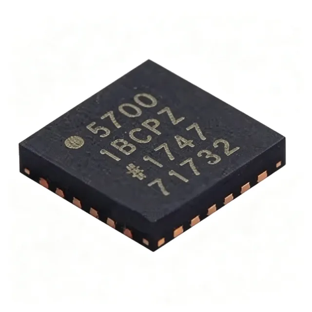
AD5700-1BCPZ - HART FSK Modem IC | Analog Devices
The AD5700-1BCPZ is a single-chip HART FSK half-duplex modem from Analog Devices, designed to comply with the HART physical layer requirements. It integrates all necessary filtering, signal detection, modulation, demodulation, and signal generation functions, requiring few external components. The device operates from a 2.7V to 5.5V supply and features an internal oscillator, eliminating the need for an external crystal. It is available in a compact 24-lead LFCSP-WQ (4x4 mm) package, making it ideal for space-constrained industrial applications. A HART modem is a specialized integrated circuit that enables communication over legacy 4-20 mA analog loops by superimposing a digital frequency-shift keying (FSK) signal. The HART protocol uses two frequencies: 1200 Hz for logic '1' and 2200 Hz for logic '0', allowing simultaneous analog and digital communication. The AD5700-1BCPZ is part of the HART modem product family, which falls under the broader category of industrial communication ICs, specifically interface ICs for process automation. Key features of the AD5700-1BCPZ include a low power consumption of 1 mA typical, an integrated receive band-pass filter that can be bypassed, and an internally buffered HART output with high drive capability. The device also includes an internal 2.5V reference and supports a wide operating temperature range of -40°C to +125°C. The LFCSP package provides excellent thermal performance and a small footprint, suitable for high-density designs. Technically, the AD5700-1BCPZ uses a digital signal processing (DSP) architecture to implement the HART modem functions, ensuring accurate and reliable communication. The integrated filter eliminates the need for external components, simplifying the design and reducing bill of materials cost. The device is fully compliant with the HART physical layer specification, ensuring interoperability with other HART-compliant devices. Typical applications include industrial process control, smart transmitters, valve positioners, and other field instruments that require HART communication. The low power consumption and small package make it suitable for loop-powered devices where power budget is critical. The internal oscillator further reduces component count, making it an excellent choice for compact designs. When designing with the AD5700-1BCPZ, ensure proper decoupling of the power supply and careful layout of the analog and digital sections to minimize noise. The device requires a few external components, including a coupling capacitor and a protection circuit for the HART signal path. Refer to the datasheet for detailed application circuits and recommended component values.
AD5700-1BCPZ-RL - HART Modem IC with Oscillator | Analog Devices
The AD5700-1BCPZ-RL is a single-chip HART FSK half-duplex modem from Analog Devices, designed to comply with the HART physical layer requirements. It integrates all necessary filtering, signal detection, modulation, demodulation, and signal generation functions, requiring few external components. The device operates from a 2.7V to 5.5V supply and features an integrated oscillator, eliminating the need for an external crystal. It is available in a compact 24-lead LFCSP-WQ (4x4 mm) package, suitable for space-constrained industrial applications. A HART modem is a specialized integrated circuit that enables communication over legacy 4-20 mA analog loops by superimposing a frequency-shift keying (FSK) digital signal. The AD5700-1 is part of the HART modem product family, which falls under the broader category of industrial communication ICs. These devices are essential in process automation, allowing digital configuration and diagnostics without disrupting analog measurement signals. Key features include a low-power design with a typical supply current of 86 µA in listen-only mode, an integrated receive band-pass filter that can be bypassed, and an internally buffered HART output for high drive capability. The device also includes an internal reference, a RESET pin for power-down mode, and a REF_EN pin to control the internal reference. The integrated oscillator provides a precise 1.2 MHz clock, simplifying the design and reducing component count. The AD5700-1 uses a digital signal processing (DSP) architecture to implement the HART protocol, ensuring reliable communication over long cable runs. The device supports data rates of 1200 bps, the standard HART speed, and is fully compliant with the HART physical layer specification. The LFCSP package offers excellent thermal performance and a small footprint, making it ideal for loop-powered transmitters and other compact field instruments. Typical applications include industrial process control, smart transmitters, valve positioners, and other field instruments that require HART communication. The device interfaces easily with Analog Devices' industrial converters, such as the AD5421 loop-powered current-output DAC, enabling complete smart transmitter solutions. When designing with the AD5700-1, ensure proper decoupling on the supply pins and follow the recommended layout in the datasheet to minimize noise. The RESET pin can be used to place the device in power-down mode, reducing current consumption to 1 µA, which is critical for loop-powered applications.
AD5700-1BCPZ-RL7 - Low Power HART Modem | Analog Devices
The AD5700-1BCPZ-RL7 is a single-chip HART FSK half-duplex modem from Analog Devices, designed to meet HART physical layer requirements for industrial field instrumentation. Housed in a 24-LFCSP-WQ (4x4) package, this low-power modem operates from a 1.71 V to 5.5 V supply and draws a maximum of 115 µA in receive mode, making it suitable for loop-powered and intrinsically safe applications. The AD5700-1 variant integrates a precision internal oscillator, eliminating the need for an external crystal and reducing component count and board area. A HART modem is a communication IC that superimposes digital Frequency Shift Keying (FSK) signals onto a 4-20 mA analog current loop, using 1200 Hz and 2200 Hz sinusoidal tones to represent logic '1' and logic '0'. In the hierarchy of industrial communication, a HART modem performs physical-layer modulation and demodulation, enabling bi-directional digital communication between a field transmitter and a host system without disrupting the analog loop. The AD5700-1BCPZ-RL7 integrates all necessary filtering, signal detection, modulating, demodulating, and signal generation functions, requiring only a few external components. Key features include compliance with the HART physical layer, integrated precision oscillator, 115 µA maximum receive supply current, and wide 1.71 V to 5.5 V operating range. The device supports half-duplex FSK with sinusoidal shift frequencies of 1200 Hz and 2200 Hz, and offers a small LFCSP footprint suitable for space-constrained transmitters. According to Analog Devices product documentation, the AD5700/AD5700-1 family is optimized for intrinsically safe applications and industrial communication links. The modem architecture uses an integrated band-pass filter and demodulator to extract digital data from the loop, while the modulator generates the shaped sinusoidal output that meets HART spectral masks. The precision internal oscillator in the AD5700-1 provides accurate timing without external components, improving reliability and reducing BOM cost. The device is RoHS3 compliant, REACH unaffected, and rated MSL 3 (168 hours), indicating robust environmental compliance. Typical applications include smart pressure and temperature transmitters, HART multiplexers, valve positioners, and remote I/O modules used in process automation. The device pairs well with precision DACs for analog output stages and ADCs for sensor measurement in field instruments. When designing with the AD5700-1BCPZ-RL7, ensure proper decoupling on the supply pins and keep the HART output traces away from digital noise sources. Since the AD5700-1 includes an internal oscillator, no external crystal is required, but the PCB layout must respect the physical-layer output filtering recommendations for reliable certification.
AD725ARZ-R7 - RGB to NTSC/PAL Video Encoder | Analog Devices
The Analog Devices AD725ARZ-R7 is a very low cost general purpose RGB to NTSC/PAL video encoder IC housed in a 16-pin SOIC (0.295 in / 7.50 mm width) surface-mount package, supplied in tape-and-reel packaging (the -R7 suffix). It converts red, green, and blue color component signals into their corresponding luminance (baseband amplitude) and chrominance (subcarrier amplitude and phase) signals in accordance with either NTSC or PAL standards. A video encoder is an interface IC that sits at the boundary between a digital or analog graphics source and a standard-definition composite video display. In the signal-chain hierarchy, it belongs to the video encoder -> video interface -> mixed-signal IC category, translating RGB component video into the composite waveforms that analog TVs, monitors, and recording equipment expect. Key features include simultaneous composite video output and separate chrominance and luminance (S-Video) outputs, a luma trap port that eliminates cross-color artifacts, TTL-compatible logic levels for direct interfacing with standard digital circuitry, and an integrated chroma delay line. These functions normally require several external components in discrete implementations; the AD725 integrates them on chip, which is the basis of its very low system cost. Technically, the AD725 performs analog matrixing of the RGB inputs into the Y (luminance) and quadrature-modulated C (chrominance) components, with a subcarrier locked to an external color burst crystal reference. The luma trap port allows the designer to notch the chroma subcarrier from the luma path, preventing cross-color artifacts on high-saturation images. NTSC or PAL operation is selected by pin strapping, and the integrated delay ensures the luma and chroma signals re-align at the output, preserving horizontal picture resolution. Typical applications include embedded graphics systems that must drive legacy composite monitors, industrial HMI and test-equipment video outputs, set-top and retro-computing video interfaces, and automotive or kiosk displays that accept only NTSC/PAL composite or S-Video input. A key design consideration is crystal accuracy: the NTSC (3.579545 MHz) or PAL (4.433619 MHz) subcarrier crystal must be within specification to keep color hue and saturation stable, and analog ground and power routing should keep RGB input noise below the encoder's signal swing to preserve picture quality. This page synthesizes distributor availability data, verified datasheet features, drop-in alternatives, and practical design guidance not consolidated in the manufacturer datasheet alone.
AD725ARZ-RL - RGB to NTSC/PAL Video Encoder | Analog Devices
The Analog Devices AD725ARZ-RL is a low-cost RGB to NTSC/PAL video encoder IC that converts red, green, and blue color component signals into their corresponding luminance and chrominance signals in accordance with either NTSC or PAL standards, housed in a 16-pin SOIC (7.50 mm width) surface-mount package delivered in tape-and-reel packaging. A video encoder is a mixed-signal device in the data conversion and video interface hierarchy that transforms parallel or analog component video (RGB or YUV) into a single composite baseband video signal, or into separate luminance (Y) and chrominance (C) signals for S-Video. Encoders sit between a graphics processor or video source and a TV monitor, VCR, or video capture input, performing the color-space conversion, subcarrier modulation, and sync generation required by broadcast television standards. Key features of the AD725 include both NTSC and PAL composite video outputs and separate chrominance and luminance (S-Video) outputs from the same device, a luminance trap (YTRAP) port that reduces cross-color artifacts generated by subcarrier-frequency components present in the luminance signal, fully TTL-compatible logic levels that support 3 V CMOS logic requirements, and an integrated luminance delay line. This combination allows a single, very low cost device to serve as the complete analog video output stage for embedded systems. Technically, the AD725 performs RGB-to-YUV matrix conversion, quadrature modulation of the color difference signals onto a subcarrier, and sync insertion, producing standard-amplitude baseband video. For portable or other power-sensitive applications, the device can be powered down to less than 1 uA of current consumption, which is exceptionally low for a video-grade mixed-signal encoder. Typical applications include embedded graphics boards, set-top box video outputs, industrial display interfaces, legacy TV-out ports on microprocessor systems, and video test equipment where NTSC or PAL composite output is required from an RGB source. A key design consideration is proper use of the YTRAP pin: connecting the correct external LC trap circuit suppresses subcarrier leakage into the luminance path and materially reduces cross-color shimmer on fine luma detail. Supply decoupling and standard-accuracy crystal reference for the color subcarrier are also important for color accuracy. This page synthesizes distributor pricing, drop-in alternatives, practical design notes, and application guidance not found in the manufacturer datasheet alone.

ADG1204YCPZ-500RL7 - ±15V/+12V 4:1 iCMOS Multiplexer, 12-LFCSP
The Analog Devices ADG1204YCPZ-500RL7 is a monolithic CMOS analog multiplexer comprising four single channels in a 4:1 (SP4T) configuration, built on Analog Devices' iCMOS (industrial CMOS) modular process that combines high-voltage CMOS with bipolar technologies. The device operates from a single analog supply of ±15 V or +12 V dual analog rails, with rail-to-rail signal handling and 3 V logic-compatible digital inputs, eliminating the need for a separate VL supply rail. Housed in a 12-lead LFCSP (3x3 mm) package with an exposed pad, it delivers an on-resistance of 190 Ω typical and ultra-low 1.5 pF off source capacitance. An analog multiplexer (mux) is a precision solid-state switch that routes one of multiple analog input channels to a common output under digital control. Within the broader signal-chain hierarchy, an analog mux sits between the analog front end (sensors, instrumentation amplifiers) and the data converter (ADC), occupying the same functional niche as a relay matrix but with orders-of-magnitude faster switching and no mechanical wear. Multiplexers like the ADG1204 trade raw RF bandwidth for very high DC accuracy and charge-injection performance, which is why they dominate precision data-acquisition and sample-and-hold front ends. Key features include <1 pC charge injection when switching channels (critical for glitch-free sample-and-hold), 33 V maximum supply range, fully specified rail-to-rail operation, fully specified ±15 V/+12 V performance, and 3 V logic-compatible inputs that interface directly to modern FPGAs and microcontrollers without level shifters. iCMOS construction ensures ultralow power dissipation in a footprint compatible with portable instrumentation. The exposed pad of the LFCSP-12 package provides a low-thermal-resistance path to PCB copper, supporting reliable operation across the -40 °C to +125 °C automotive/industrial temperature range. Architecturally, the ADG1204 uses four independent NMOS transmission gates with break-before-make switching and TTL/CMOS-compatible address logic. The sub-1 pC charge injection is achieved through a proprietary switch-driver topology that cancels the gate-drain overlap charge, making the device suitable for sample-and-hold applications where channel-to-channel switching transients would otherwise corrupt the held voltage. Typical applications include precision data acquisition front ends, sample-and-hold amplifiers, automated test equipment (ATE) channel selection, audio/video signal routing, and battery-powered instrumentation where the iCMOS low-power advantage matters most. The 3x3 mm LFCSP footprint also makes it a strong fit for space-constrained multi-channel designs. When designing with the ADG1204, observe that the on-resistance of 190 Ω is not constant across the signal range - it varies with VDS and is highest near the rails. For low-distortion audio applications, keep signal amplitudes within ±5 V of mid-supply where RON flatness is best. The exposed pad must be soldered to a sufficient ground plane to keep junction temperature within spec; thermal vias to internal ground layers are strongly recommended. This page synthesizes distributor pricing, drop-in alternatives, and practical design notes not found in the manufacturer datasheet alone.
ADG1204YCPZ-REEL7 - ±15V 4:1 iCMOS Mux, 190Ω, 12-LFCSP | ADI
The Analog Devices ADG1204YCPZ-REEL7 is a low-capacitance, low-charge-injection, monolithic CMOS analog multiplexer configured as a 4:1 single-pole four-throw (SP4T) switch, with an on-resistance of 190 Ω and packaged in a 12-lead LFCSP (3 mm × 3 mm). It operates from dual ±15 V supplies or a single +12 V supply, making it suitable for industrial analog signal chains where bipolar headroom is required. An analog multiplexer (MUX) is a semiconductor switch that routes one of multiple analog input signals to a common output line under digital logic control, and it sits within the broader category tree of analog switch -> multiplexer/demultiplexer -> interface IC -> integrated circuit. The ADG1204 uses ADI's iCMOS (industrial CMOS) process, which combines high-voltage CMOS and bipolar transistors on a single die to deliver ±15 V signal swings with the low power dissipation typical of CMOS logic. Key features include ultralow charge injection (typically < 1 pC), low on-capacitance for minimal signal distortion at high frequency, fast switching speed with a bandwidth suitable for video signals, and a break-before-make action that eliminates momentary shorting between adjacent channels. The digital interface accepts standard TTL/CMOS logic levels at the A0 and A1 address pins plus an active-low EN to put the device into a high-impedance state when disabled. Architecturally, the ADG1204 integrates four independent n-channel MOSFET pass gates whose sources connect to the common D pin and whose drains terminate at the four S1–S4 pins, with logic translation circuitry ensuring that 3 V microcontroller GPIO can reliably drive the part from ±15 V analog rails. The iCMOS process also enables latch-up immunity under over-voltage transients. Typical applications include data-acquisition front ends, sample-and-hold circuits, video signal routing, ATE (automatic test equipment) pin switching, and precision instrumentation multiplexers. The wide supply tolerance allows direct interfacing to ±12 V or ±15 V op-amp outputs in industrial control loops. When designing with this device, ensure logic levels at the address pins remain within 0 V to VDD regardless of analog signal swing, and place 0.1 µF decoupling capacitors as close as possible to each supply pin. The exposed pad on the LFCSP package must be soldered to the PCB ground plane to achieve the rated power dissipation and to maintain the specified on-resistance stability. This page synthesizes distributor pricing, drop-in pin-compatible alternatives, and practical PCB design notes not found in the standalone ADI datasheet.

ADG1206YCPZ-REEL7 - 16:1 iCMOS Mux, Low Cap, ±15V/12V | ADI
The Analog Devices ADG1206YCPZ-REEL7 is a monolithic iCMOS analog multiplexer that switches one of sixteen inputs to a common output, controlled by 4-bit binary address lines A0, A1, A2, and A3, and is housed in a 32-lead LFCSP-WQ (5 mm × 5 mm) package with on-resistance of 200 Ω maximum. It is built on Analog Devices' iCMOS process technology, which combines high-voltage CMOS, bipolar, and DMOS elements to deliver ±15 V / +12 V dual supply operation with ultralow power dissipation and ESD protection. The part is supplied on a 7-inch reel (-REEL7) and is specified over the -40 °C to +125 °C extended industrial temperature range. A multiplexer (MUX) is a switching component that selects one of multiple analog input signals and forwards the chosen channel to a single output line, controlled by a digital address. MUX devices sit within the broader signal-chain hierarchy: analog switch → multiplexer → data-acquisition front-end → mixed-signal subsystem. The 16:1 configuration implemented in the ADG1206 is the single-ended counterpart to the differential 8:1 ADG1207, both built on the same iCMOS die family. Key specifications include 200 Ω on-resistance (max), 13 pF typical on-capacitance, 490 MHz -3 dB bandwidth, 75 ns tON / 85 ns tOFF transition times, and ±15 V or +12 V single-supply operation. Ultralow charge injection (typically <1 pC) and low parasitic capacitance make it well-suited for data-acquisition front-ends, sample-and-hold circuits, and precision instrumentation where minimal signal-glitch and fast settling are required. The LFCSP-WQ-32 package includes an exposed thermal pad that must be soldered to the PCB ground plane for proper thermal and electrical performance. The iCMOS architecture allows ±15 V analog signal swings while running from a low-voltage logic interface, eliminating the need for external level shifters. The latch-up-immune construction and ESD robustness exceed 4 kV HBM on the analog inputs, making the part tolerant of harsh industrial environments. Designers should note that the ADG1206YCPZ-REEL7 and the ADG1206YCPZ (tray) are the same die in different packaging media; the only difference is the carrier format (reel vs. tray) for high-volume assembly. Typical applications include automated test equipment (ATE) and switching matrices, data-acquisition systems, sample-and-hold amplifiers, medical imaging front-ends, communication system routing, and avionics signal multiplexing. The wide analog signal range and low distortion also suit audio routing and video switching designs. For battery-powered or precision portable instruments, the ultralow power dissipation (typically <0.5 µW quiescent) extends operating life. A key design consideration is the analog ground (AGND) and digital ground (DGND) pin arrangement: the LFCSP-WQ-32 package provides separate analog and digital ground pins that should be tied to a low-impedance ground plane to minimize crosstalk between the digital address lines and the analog signal path. Designers must also observe the absolute maximum analog input voltage of ±25 V with respect to AGND, even when the supplies are off, to avoid latch-up. This page synthesizes manufacturer datasheet parameters, distributor pricing as of 2026-10-06, drop-in cross-references, and practical design notes not consolidated in any single vendor listing, providing unique value beyond Digi-Key or Mouser product pages.
ADG1207YCPZ - Low Cap 8-Ch ±15V iCMOS Mux | Analog Devices
The Analog Devices ADG1207YCPZ is a monolithic iCMOS analog multiplexer integrating eight differential channels in a 32-lead LFCSP-WQ (5x5 mm) package with 200 ohm on-resistance and ultra-low 1.5 pF off capacitance. It switches one of eight differential inputs to a common differential output, addressed by a 3-bit binary code on A0, A1, and A2, and operates from dual ±5 V to ±15 V supplies or a single 12 V supply with up to 33 V total range. An analog multiplexer (mux) is a semiconductor switch that routes one of multiple analog input signals to a single output line under digital control, forming the front-end of a data acquisition system. In the hierarchy of signal-chain components, the mux sits between sensors or transducers and downstream amplifiers or converters, and as a member of the analog switch IC family it is valued for low on-resistance, low capacitance, and fast settling. The ADG1207 belongs specifically to the iCMOS process family, which combines high-voltage CMOS with sub-micron logic to achieve low power and small footprint simultaneously. Key differentiating features include less than 1 pC charge injection over the entire signal range, rail-to-rail signal handling, break-before-make switching action that prevents momentary shorting between channels, and TTL/CMOS-compatible 3 V logic inputs that interface directly to modern microcontrollers and FPGAs. The wide 33 V supply range supports industrial ±15 V systems as well as single-supply 12 V designs, and the 200 ohm on-resistance remains flat across the signal range, minimizing distortion in precision paths. The device uses iCMOS construction, an Analog Devices process technology that places a high-voltage analog transistor layer on top of a sub-micron CMOS logic layer. This allows the analog switches to handle ±15 V signals while the address decoders operate at sub-5 V CMOS levels, achieving ultralow power dissipation and latch-up immunity in a compact surface-mount package. Typical applications include data acquisition front-ends, sample-and-hold circuits, automatic test equipment (ATE) signal routing, audio and video signal switching, battery-powered instrumentation, and avionics multiplexing. The differential 8:1 architecture is particularly suited for balanced signal chains such as professional audio, instrumentation amplifiers, and isolated ADC front-ends where common-mode rejection matters. When designing with the ADG1207YCPZ, ensure the address lines are stable before VDD ramps to avoid parasitic channel selection during power-up, and place 100 nF decoupling capacitors close to each supply pin. For highest DC accuracy in low-impedance loads, select the ADG1407 family instead, since the ADG1207's 200 ohm on-resistance dominates error in sub-kohm paths. This page synthesizes distributor pricing, verified drop-in alternatives, and practical design notes not found in the standalone datasheet, giving engineers a single source for selection, sourcing, and layout guidance.

ADG1208YRUZ-REEL7 - 8:1 iCMOS MUX, 16-TSSOP | Analog Devices
The Analog Devices ADG1208YRUZ-REEL7 is a monolithic, single 8-to-1 analog multiplexer built on Analog Devices' iCMOS (industrial CMOS) process, packaged in a 16-pin TSSOP (YRU) with a 200 ohm on-resistance. It switches one of eight analog inputs to a common output as determined by 3-bit binary address lines A0, A1, and A2, operating from dual +/-5 V to +/-15 V supplies or a single +12 V supply across a 33 V supply range. An analog multiplexer is a semiconductor switch that routes one of multiple analog input signals to a single output line under digital control. MUXes belong to the broader category of analog switches and multiplexers, which sit under interface ICs and are essential building blocks in data acquisition (DAQ), instrumentation, audio routing, and automatic test equipment (ATE). The ADG1208's iCMOS process combines high-voltage CMOS with submicron CMOS, providing low power consumption, low on-resistance, and high switching speed in a small footprint. Key features include 200 ohm on-resistance (160 ohm per third-party sources), 5 ohm on-resistance flatness, +/-15 V dual supply operation, 1 pC charge injection, 2 pF off capacitance, 75 dB off-isolation, and 60 ns transition time. The device also offers break-before-make switching, rail-to-rail operation, 3 V logic-compatible digital inputs, and fully specified performance with +/-5 V, +5 V, +/-12 V, or +12 V supplies. The ADG1208 employs parallel CMOS switches with parasitic-junction-isolated bodies, enabling low charge injection and low capacitance. The wide supply range supports industrial signal levels up to +/-15 V while the 3 V logic interface allows direct connection to modern microcontrollers, FPGAs, and ADCs without level shifters. Typical applications include data acquisition front-ends, sample-and-hold systems, PLC analog input modules, ATE signal routing, audio/video signal switching, and battery-powered instrumentation. The TSSOP-16 footprint suits space-constrained PCB designs. When designing with the ADG1208, add 0.1 uF bypass capacitors near each supply pin and ensure unused digital address lines are tied to GND or VDD to avoid floating-state channel selection. The break-before-make architecture prevents momentary shorting between channels during switching transitions. This page synthesizes verified distributor pricing, pin-compatible drop-in alternatives, and application-specific design guidance not consolidated in the manufacturer datasheet, providing an engineering decision aid for sourcing and design-in.
ADG1213YRUZ - Quad SPST iCMOS Switch, 120Ω, ±15V | Analog Devices
The Analog Devices ADG1213YRUZ is a monolithic iCMOS (industrial CMOS) quad SPST (Single-Pole Single-Throw) analog switch housed in a 16-pin TSSOP (YRU) package, featuring 1 pF off capacitance, 2.6 pF on capacitance, <1 pC charge injection, and 120 Ω on resistance. It operates from ±4.5 V to ±16.5 V dual supplies or up to +12 V single supply with rail-to-rail signal handling and 33 V maximum supply range. An iCMOS switch is a monolithic CMOS device that combines high-voltage CMOS and bipolar process steps, enabling analog switches that tolerate ±15 V supplies while still allowing 3 V logic-compatible control inputs without requiring a separate V_L rail. The ADG1211/ADG1212/ADG1213 family sits in the broader hierarchy of analog switches → multiplexers → signal-chain interface ICs → mixed-signal semiconductors, and serves as a precision, low-charge-injection building block between sensitive analog front ends and higher-voltage analog signal paths. Key differentiating features include four independently selectable normally-open SPST channels (the ADG1211 is normally-open, ADG1212 normally-closed, ADG1213 contains two of each - check device grade), sub-1 pC charge injection that minimizes transient switching disturbance on sample-and-hold capacitors, and typical power consumption below 0.03 µW, making it well suited for power-sensitive multi-channel instrumentation. The 120 Ω on resistance is fully specified at ±15 V and +12 V with a flat, low-distortion characteristic across the audio band. Architecturally, the ADG1213 leverages the iCMOS process to integrate high-voltage DMOS transistors alongside low-voltage CMOS logic on a single die, eliminating the need for a logic-level shifter supply and simplifying board-level power-tree design. Each switch is independently controlled by a TTL/CMOS-compatible digital input, and all four channels exhibit matched on-resistance and ton/toff timing for synchronized multi-channel sampling. Typical applications include precision data-acquisition front ends, audio and video signal routing, automated test equipment (ATE) multiplexers, medical instrumentation, communication systems, and battery-powered multi-channel sensor switching where charge injection and input capacitance directly affect measurement integrity. When designing with this device, place 0.1 µF or larger decoupling capacitors as close as possible to the VDD and VSS pins, and keep digital control traces isolated from analog signal paths to preserve the low charge-injection and low distortion performance. The TSSOP-16 footprint is compatible with ADG1211YRUZ and ADG1212YRUZ variants for design reuse across NC/NO options. This page synthesizes distributor pricing, drop-in alternatives, and practical design notes not found in the manufacturer datasheet, providing a single-source engineering reference for the ADG1213YRUZ.

ADG1219BRJZ-REEL7 - ±15V/12V iCMOS SPDT Switch SOT-23-8 | Analog Devices
The Analog Devices ADG1219BRJZ-REEL7 is a monolithic iCMOS SPDT (single-pole double-throw) analog switch housed in an 8-pin SOT-23 package, featuring an active-low EN input that simultaneously disables both channels. The device is fully specified at +12 V single supply and ±15 V dual supply rails, exhibits a low 200 ohm on resistance, less than 0.5 pC charge injection over the full signal range, and 2.5 pF off capacitance, making it well-suited for precision signal-chain switching in industrial and instrumentation systems. A SPDT (single-pole double-throw) analog switch is a fundamental building block of the analog switch and multiplexer family. It routes one input signal to one of two outputs, or vice versa, using MOSFET pass transistors controlled by a logic-level input. SPDT switches sit within the broader taxonomy of analog switches -> multiplexers -> interface ICs -> signal conditioning, where they are valued for their bidirectional signal paths, near-zero quiescent current, and ability to handle rail-to-rail analog signals. The iCMOS (industrial CMOS) process used in the ADG1219 allows high-voltage bipolar swings (±15 V / 12 V) on a monolithic CMOS die, combining low power consumption with the wide dynamic range traditionally reserved for junction-isolation processes. Key features that differentiate this part include break-before-make switching action that prevents momentary shorting between channels during transitions, a low 0.6 nA maximum off leakage current at 85 °C, and 3 V to 16.5 V single-supply operation without requiring a logic-level VL supply. The 2.5 pF off capacitance and sub-1 pC charge injection make the ADG1219 well matched to data-acquisition front ends where injected charge would otherwise corrupt sample-and-hold settling. Typical application circuits include audio signal routing, ATE (automatic test equipment) channel selection, video switching, precision data-acquisition multiplexers, and battery-powered instrumentation. The enable pin simplifies power-down sequencing in multi-channel systems, allowing designers to put unused switches into a high-impedance state with a single control line. When designing with this part, place 0.1 µF decoupling capacitors close to VDD and VSS pins to suppress logic-induced transients. Because the switch is bidirectional, source and drain terminals are interchangeable, simplifying PCB layout. For applications that exceed ±15 V signals, review the absolute maximum ratings in the manufacturer datasheet. This page synthesizes distributor pricing, drop-in alternatives, and practical design notes not found in the manufacturer datasheet alone.
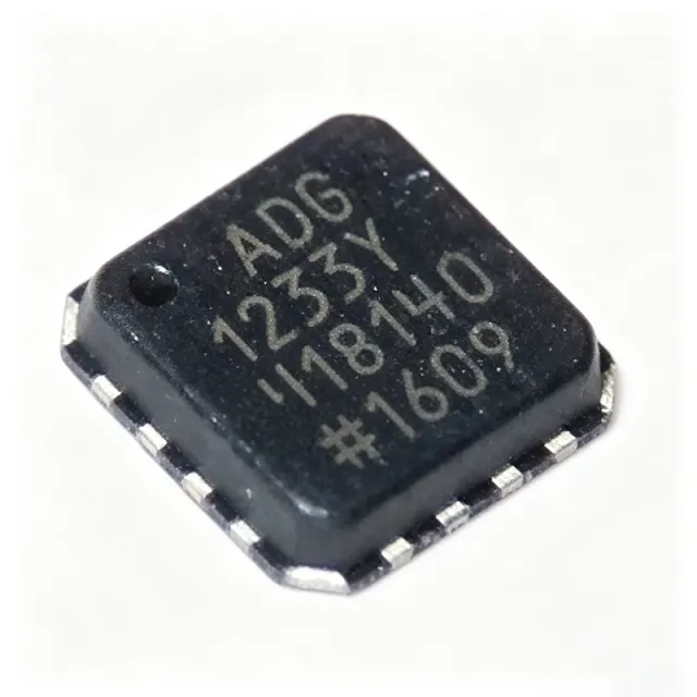
ADG1233YCPZ-REEL7 - Triple SPDT Analog Switch | Analog Devices
The ADG1233YCPZ-REEL7 is a monolithic iCMOS® analog switch from Analog Devices, integrating three independently selectable single-pole, double-throw (SPDT) switches in a compact 16-lead LFCSP-VQ (4x4 mm) package. It operates over a wide supply range of ±15 V or +12 V, with a low on-resistance of 120 Ω (typical) and ultra-low capacitance of 1.5 pF off capacitance, making it ideal for high-performance signal routing in precision instrumentation, audio, and data acquisition systems. An analog switch is a semiconductor device that selectively connects or disconnects an analog signal path under digital control. It is a fundamental building block in signal routing, multiplexing, and sample-and-hold circuits. The ADG1233 belongs to the family of analog switches and multiplexers, which are part of the broader category of interface ICs and signal conditioning components. Its iCMOS® (industrial CMOS) process technology ensures low power consumption and high voltage handling, bridging the gap between traditional CMOS and higher-voltage bipolar processes. Key features include break-before-make switching action, which prevents momentary shorting when switching channels, and an EN input that enables or disables the entire device. The switch is fully specified with 3 V logic-compatible inputs, allowing direct interface with low-voltage digital controllers. Rail-to-rail operation ensures minimal signal distortion across the full supply range. The 1.5 pF off capacitance and 0.5 pC charge injection minimize signal degradation in high-frequency and precision applications. The ADG1233 utilizes a proprietary iCMOS® process that combines the advantages of high-voltage CMOS with low power dissipation. This architecture enables the device to handle ±15 V supplies while maintaining low leakage currents and fast switching speeds. The break-before-make action is implemented through internal timing circuitry, ensuring reliable channel isolation during transitions. The device is available in a 16-lead LFCSP-VQ package, which offers excellent thermal performance and a small footprint for space-constrained designs. Typical applications include audio signal routing, precision data acquisition systems, automatic test equipment (ATE), and medical instrumentation. The low capacitance and charge injection make it particularly suitable for high-speed analog signals, while the wide supply range accommodates both bipolar and single-supply designs. The EN pin provides a convenient means of power-down or signal isolation in multi-channel systems. When designing with the ADG1233, ensure that the digital control signals are within the specified logic thresholds and that the supply voltages are properly decoupled with 0.1 µF capacitors close to the VDD and VSS pins. The break-before-make feature eliminates the need for external timing circuits, but the user should verify that the switching time meets system requirements.