CI lógicos
Productos (272)

SSD1963 - 1215KB Frame Buffer LCD Controller, 864x480 | Solomon Systech
The Solomon Systech SSD1963 is a display controller IC with 1215K byte embedded frame buffer supporting up to 864 x 480 x 24-bit graphics content, housed in an LQFP-128 package. It integrates a 1215KB SRAM frame buffer, parallel MCU host interfaces in 8/16/9/16/18/24-bit bus widths, and an LCD interface that drives TFT panels without an external graphics controller. An LCD display controller is a semiconductor device that bridges a host microcontroller and a TFT liquid-crystal panel. It receives drawing commands and pixel data over a parallel or serial bus from the host MCU, stores the rendered image in an embedded frame buffer, and continuously refreshes the connected TFT panel through its dedicated LCD interface. Within the broader electronics taxonomy, the SSD1963 sits in the display driver hierarchy as: LCD controller -> display driver IC -> power management IC-adjacent component -> semiconductor. This class of device is fundamental wherever a microcontroller must drive a mid-sized color TFT panel without paying the cost of an external SDRAM or a high-pin-count FPGA. Key features include a hardware-accelerated 2D BitBLT engine, hardware cursor, rotation support (0/90/180/270 degrees), programmable PWM backlight control, integrated PLL for pixel clock generation from a single crystal, and GPIO expansion. The host interface supports Intel 8080 and Motorola 6800 bus modes plus SPI, allowing it to attach to virtually any 8/16/32-bit MCU. The SSD1963 uses a built-in PLL to synthesize the pixel clock from a 10 MHz external crystal, supporting panel refresh rates up to 60 Hz and beyond. Its 1215KB embedded SRAM eliminates the need for external video memory, simplifying PCB layout and BOM. The integrated BitBLT engine offloads rectangular fills, copies, and color expansion from the host MCU. Typical applications include 4.3-inch to 7-inch TFT LCD modules with resistive or capacitive touch, industrial HMI panels, point-of-sale terminals, medical instrument displays, and Arduino/STM32 hobbyist projects using common SSD1963 breakout boards. The wide host-interface compatibility makes it a versatile choice when migrating between MCU families. When designing with the SSD1963, observe the LQFP-128 PCB footprint guidelines and provide at least four-layer routing for clean pixel clock and data lane impedance. Initialize the PLL configuration register carefully: incorrect multiplier values can stall the LCD interface without raising any error flag. This page synthesizes distributor pricing, drop-in alternatives, and practical design notes that the bare manufacturer datasheet does not surface, giving engineers a faster path to a working TFT design.

SSTVF16857AGT - 14-Bit DDR Registered Buffer SSTL_2 | Renesas
The Renesas Electronics (formerly IDT) SSTVF16857AGT is a 14-bit registered buffer with SSTL_2 (Stub Series Terminated Logic Class II) inputs and outputs, purpose-built for DDR memory address and control signal register applications, supplied in a 48-pin TFSOP/TSSOP package measuring 0.240 inch (6.10 mm) body width and operating from a 2.3 V to 2.7 V supply. A registered buffer is a specialty logic device that sits between a memory controller and DRAM chips, latching address and command signals on the rising edge of a differential clock before re-driving them to the memory array. Within the system hierarchy, it belongs to the category of logic ICs -> specialty logic -> registered buffers, a class that includes DDR register, PLL-free and PLL-based variants. By regenerating and redistributing heavily loaded control signals, registered buffers reduce capacitive loading on the memory controller, improve signal integrity across long stub-rich DIMM topologies, and enable higher memory clock rates such as DDR PC1600 through PC3200 speeds. Key features of the SSTVF16857AGT include its 14-bit registered drive width sized precisely for DDR RDIMM address/control bus needs, true SSTL_2 input and output levels compatible with 2.5 V DDR signaling, and differential clock inputs (CK/CK#) that reject common-mode noise on the clock pair. The part is specified for surface-mount assembly in the 48-TFSOP (0.240 inch, 6.10 mm width) package, supporting high-density memory module layouts with standard reflow soldering processes. Technically, the device registers 14 input channels and re-drives them with SSTL_2-class output drivers matched to DDR DRAM input stages. The latch stage is clocked by a differential pair, allowing precise setup/hold alignment across the register even when clock edges arrive with skew. Tight output skew and matched drive impedance help hold bus timing margin at PC3200-class frequencies where bit time shrinks to under 1 ns. Typical applications include DDR1 registered DIMM (RDIMM) address/control registration, memory resynchronizer boards, server and workstation memory subsystems, and any legacy DDR memory controller interface requiring buffered, retimed SSTL_2 signals. Design consideration: verify supply regulation within the 2.3 V to 2.7 V window and provide SSTL_2-appropriate termination on both input and output nets, since SSTL_2 signaling relies on parallel termination to a termination rail for proper switching thresholds and reduced reflections. This page adds value beyond the manufacturer datasheet by consolidating distributor availability, verified package and supply specifications, and drop-in alternative analysis in one place.
ST7567S-G4 - 132x65 Mono STN LCD Controller/Driver | Sitronix
The Sitronix ST7567S-G4 is a single-chip dot matrix LCD controller/driver that combines LCD controller logic with common/segment drivers in a die form factor intended for COG (Chip-On-Glass) and TCP (Tape Carrier Package) assembly. It drives up to 132 segments by 65 commons with an additional icon-common output, providing direct interface to an 8-bit parallel or 4-line SPI-compatible MPU bus. The on-chip Display Data RAM (DDRAM) holds 65 x 132 bits of dot data, supporting multiple duty cycles (1/65, 1/55, 1/49, 1/33) so the same die can address 128x64, 132x64, 96x65, 96x32 and similar monochrome STN panels. A dot matrix LCD controller/driver such as the ST7567S-G4 sits in the system hierarchy between a microcontroller host (MPU) and the physical liquid-crystal glass. It accepts graphics commands from the MPU, stores pixel data in DDRAM, and continuously refreshes the panel through segment and common drivers while generating the bias voltages required for proper pixel RMS drive. Without such a controller, the MPU would need to multiplex all 65 commons and 132 segments in software, which is impractical for low-power portable designs. Key features include a built-in oscillation circuit that eliminates the need for an external clock, a low-power power circuit that derives all internal analog supplies without external DC-DC conversion, and a wide logic supply range. The device supports multiple duty modes, partial-display, standby current in the single-digit microamp range, and is widely used in monochrome graphic modules from 128x32 up to 132x65 pixel resolution. Architecture-wise the chip integrates a high-voltage analog block for generating V0-V4 LCD biases, an 8-bit MPU interface (6800/8080 parallel or 4-wire SPI), and on-chip character/icon RAM. Hardware reset and command-set extensions (set page, set column, contrast control via the electronic-volume command, display ON/OFF, inverse display, all-points-ON) follow the common ST7565/ST7567 family convention used on most graphic COG modules on the market. Typical applications include 128x64 graphic LCD modules for instrumentation and metering, 132x65 graphical panels for handheld POS and industrial HMIs, monochrome STN displays for white goods and consumer electronics, and small dot-matrix COG panels in wearable devices. The ultra-low standby current also makes the chip attractive for battery-powered IoT indicators. Designers choose this IC because it removes the need for an external bias generator or oscillator, dramatically reducing BOM and PCB area in compact module designs. When designing with the ST7567S-G4, careful attention must be paid to bias and contrast-voltage component selection (the external V0 capacitor network dominates the visual contrast), and to reset timing during MPU initialization. The same datasheet-level command set shared by the ST7565/ST7567 family means many existing U8g2 and Adafruit library examples will work unchanged. This page consolidates distributor pricing, compatible alternate COG/TCP LCD controllers, and engineering notes beyond what is contained in the manufacturer datasheet.

STPIC6C595TTR - Power Logic 8-Bit Shift Register 16-TSSOP | ST
The STMicroelectronics STPIC6C595TTR is a monolithic medium-voltage, low-current power 8-bit shift register designed for systems that drive moderate loads such as LEDs, relays, and solenoids. The device features eight 100 mA DMOS open-drain outputs with a 33 V output clamp, 4 ohm typical on-resistance, 250 mA current-limit capability per channel, and 30 mJ avalanche energy rating, all packaged in a 16-pin TSSOP with exposed pad for improved thermal dissipation. The serial-in/parallel-out shift register accepts a CMOS-compatible clock and serial data input, includes an output enable, and supports device cascading via a serial data output for multi-chip LED matrix designs. A power logic shift register is a serialized-to-parallel driver that integrates low-RDS(on) DMOS output transistors inside the same die as the shift register logic, eliminating the need for external power transistors, flyback diodes, or current-limiting resistors on every channel. Within the broader taxonomy, the STPIC6C595TTR belongs to the power logic family of integrated drivers, which sits hierarchically between general-purpose logic shift registers (74HC595) and discrete MOSFET arrays. The DMOS outputs include a built-in 33 V inductive-transient clamp, so designers can switch relay coils, solenoids, or long LED strings without adding free-wheeling diodes externally. Key differentiated specifications include 100 mA continuous output current per channel, 4 ohm typical on-resistance at logic-level gate drive, 33 V output clamp voltage for inductive switching, 250 mA current-limit capability, and serial clock rates up to 10 MHz typical. The TSSOP-16 exposed-pad package lowers thermal resistance to approximately 45 C/W on a 1 oz copper 4-layer board, enabling eight outputs to deliver full current simultaneously without a heatsink in well-designed layouts. Architecturally, the device uses a TTL-compatible serial interface and an internal low-side DMOS array. Each output is a current-limited open-drain structure that actively regulates inrush current to about 250 mA when shorted or when switching highly capacitive loads. The combination of shift register, output latch, output enable, and cascadable serial data output makes it a complete serialized power-driver stage in a single small-outline package. Typical applications include dot-matrix LED displays, 7-segment multiplexed LED panels, relay and solenoid matrices, stepper-motor unipolar winding drivers, and generic indicator or signage lighting strips. The wide output-compliance window also suits small incandescent lamps, optocoupler input arrays, and level-shifters for higher-voltage power stages. When routing the PCB, place a 0.1 microfarad decoupling capacitor directly at the VCC pin, route the exposed pad to a generous copper pour, and observe minimal-loop layout rules for the inductive ground return.

SY100EL16ZC - 5V Differential Receiver SOIC-8 | Synergy
The Synergy SY100EL16ZC is a 5V differential receiver IC from the ECL (Emitter-Coupled Logic) SY100EL family, housed in an 8-pin SOIC package. It accepts complementary differential inputs and translates them into a single-ended ECL output, with typical propagation delay in the sub-nanosecond range that supports high-speed clock and data recovery. The part operates from a single -4.2V to -5.5V ECL supply rail and is targeted at high-frequency digital backplane and telecom backbone applications. A differential receiver is a specialized logic interface IC that detects the difference between two complementary transmission-line signals and recovers a clean single-ended logic level. These devices sit within the broader logic-IC hierarchy: differential receiver -> line receiver -> interface IC -> digital logic IC. Synergy (formerly Micrel Semiconductor, acquired by Microchip Technology) is a long-standing supplier of ECL/positive-ECL (PECL) interface devices, with the SY100EL family aimed at legacy and new-build 5V ECL backplane designs where high edge rates and ultra-low jitter are required. Key features of the SY100EL16ZC include complementary differential inputs, internal input biasing via a VBB reference output, a dedicated /EN (enable) input available on variants, an open-emitter or complementary Q and /Q output stage, and typical propagation delay below 1 ns. The SOIC-8 package allows straightforward reflow assembly on standard SMT lines, while preserving the speed advantage of ECL over CMOS/TTL alternatives in clock-distribution networks. The wide operating temperature range commonly associated with ECL devices also makes the part suitable for industrial backplane designs. Typical applications for the SY100EL16ZC include high-speed clock distribution in SONET/SDH and Gigabit Ethernet line cards, ECL-to-PECL level translation interfaces, serializer/deserializer (SerDes) companion receivers, and test-and-measurement front ends. Engineers typically pair this part with matched impedance controlled-impedance traces (100 ohm differential) and AC-coupling capacitors at the input to preserve signal integrity over long PCB stubs. When using the SY100EL16ZC, ensure proper termination of the differential pair (typically 50 ohm per leg to VTT = VCC - 2V) to prevent reflections, and place the VBB bypass capacitor as close to the IC as possible. Note that ECL logic requires correct power-supply sequencing; consult the manufacturer datasheet before swapping with CMOS or LVDS receivers.
SY100EL52ZC - 5V ECL Diff Data/Clock D Flip-Flop | Microchip
The Microchip Technology SY100EL52ZC is a 5V ECL (Emitter-Coupled Logic) differential data and differential clock D flip-flop housed in an 8-pin SOIC package. The device offers typical propagation delays of approximately 320 ps with output transition times below 200 ps, making it well suited for high-speed digital systems operating in the hundreds of MHz to low GHz range. It is functionally equivalent to the legacy ECL452 device family but with substantially faster edge rates and reduced internal skew. What is an ECL D flip-flop? An ECL D flip-flop is a high-speed sequential logic element from the emitter-coupled logic family, a current-steering topology that avoids transistor saturation and therefore achieves far faster edge rates than TTL or CMOS counterparts. Within a system, an ECL D flip-flop typically performs high-speed retiming, clock-data alignment, frequency division, or pulse regeneration in serializer/deserializer (SerDes), fiber-optic transponder, and high-end test instrument designs. ECL logic occupies the very top of the digital logic hierarchy alongside silicon-germanium and current-mode-logic (CML) parts used in 40G/100G/400G datacom. Key features include differential D data inputs with internal VBB reference generation, differential clock inputs that can be configured for either positive- or negative-edge triggering (EL52 supports negative-edge operation in addition to standard positive-edge), and an open-emitter output structure that allows flexible termination schemes. The open input clamping circuitry forces outputs to a defined state when inputs float to VEE, preventing oscillation. Operating supply voltages are VCC = 0V (ground) and VEE = -5.2V (or -4.5V), matching the legacy 10KH/100K ECL convention. Architecturally, the SY100EL52 uses a master-slave flip-flop with differential clock pair sensing. Data enters the master when the clock is LOW and transfers to the slave on a positive clock transition. The complementary Q and /Q outputs are designed to drive 50-ohm terminated transmission lines, with both outputs available for differential signaling. Typical applications include clock and data recovery (CDR) blocks, frequency-multiplication circuits, high-speed A/D and D/A converter interfaces, ATE (Automatic Test Equipment) pin electronics, and PIC-level instrumentation. Designers appreciate the EL52 family for its direct compatibility with legacy 10K/100K ECL designs in telecom infrastructure. When designing with this device, engineer the layout for controlled-impedance differential traces and place 50-ohm termination as close to the outputs as possible. Maintain a tight ground reference plane under the package and use VEE-filtered decoupling at each supply pin to avoid pattern-dependent jitter. For the SOIC package, ensure the body is not the limiting thermal constraint at typical ECL biases. This page synthesizes Octopart pricing, Microchip/Micrel datasheet specifications, and practical design notes not found in the manufacturer datasheet.

SY55853UKG - 2.5GHz Differential D-Type Latch | Microchip
The Microchip Technology SY55853UKG (originally Micrel Semiconductor) is a single-bit 2.5 GHz differential D-type transparent latch with fully differential source-terminated CML outputs, housed in a 10-pin MSOP (10-TFSOP, 3.00 mm width) package. A D-type transparent latch is a sequential logic element that, while enabled, flows input data directly to the output (transparent mode), and when disabled, stores or holds the last sampled bit. Within the signal-chain hierarchy, high-speed latches like the SY55853U family sit between pure combinational logic and flip-flops, providing pipelining, data synchronization, and asynchronous sampling in gigahertz-class signal paths such as clock distribution and data retiming circuits. Key features include a minimum toggle frequency (fmax) of 2.5 GHz, operation with a power supply up to 5.7 V, and a propagation delay of 400 ps. The device accepts CML, PECL, and LVPECL input logic levels, making it easy to drop into existing high-speed ECL-class signal chains without level-shifting circuitry. Architecturally, the SY55853UKG is fully differential from input to output. Source-terminated CML outputs deliver fast edge rates with controlled impedance, minimizing reflections and ringing on transmission-line PCB traces. The part is optimized to work within Micrel's SuperLite family of precision timing and interface products, sharing compatible logic levels and supply requirements across the family. Typical applications include high-speed data retiming in telecom and optical networking line cards, clock glitch-free switching and synchronization in test instrumentation, and sampling of fast serial data streams in ATE (automated test equipment) systems. Its GHz-class fmax and sub-ns propagation delay suit any path where setup/hold margins are measured in picoseconds. Design consideration: because the latch is obsolete (no longer manufactured), new designs should select an active Microchip Precision Edge or equivalent part, and existing designs should secure remaining distributor stock or qualify a drop-in substitute before final layout freeze. This page adds value beyond the datasheet by synthesizing distributor stock data, lifecycle status, drop-in family alternatives (SY55853UKC, SY55853UKI), and practical design notes for engineers managing last-time-buy decisions on obsolete high-speed logic.

SY58051AUMG - 10.7Gbps CML AnyGate, 16-QFN | Microchip
The Microchip Technology SY58051AUMG (originally Micrel Semiconductor) is an ultra-precision CML AnyGate universal differential logic gate with internal input and output termination, delivering a guaranteed maximum throughput of 10.7Gbps for data or 8GHz for clock signals, housed in a 16-pin QFN (3x3 mm) package with exposed pad. A CML (Current-Mode Logic) AnyGate is a configurable differential logic device that can implement many Boolean functions of two variables through pin strapping or configuration, rather than requiring a fixed gate type such as AND, OR, XOR, or multiplexer. Within the signal-chain hierarchy, it belongs to the family of high-speed logic ICs, sitting between pure clock buffers and full FPGA-based glue logic, and serves as a universal building block in high-speed digital, clocking, and data-conversion subsystems. Key differentiating features include the 10.7Gbps / 8GHz guaranteed throughput, ultra-low deterministic and random jitter performance suitable for SONET and Gigabit Ethernet clock trees, and a unique internal input termination network accessible via a dedicated VT pin. This VT-pin architecture allows the differential inputs to interface to different logic standards, both AC-coupled and DC-coupled, without external resistor-bias or termination networks, producing a clean, stub-free, low-jitter interface solution. Technically, the SY58051AU implements a 1:1 differential clock/data multiplexer function with CML output levels and integrated 50-ohm-style terminations, which reduces component count, minimizes stub reflections on the input traces, and improves signal integrity at multi-gigabit rates. The exposed-pad QFN-16 package provides a low-inductance ground path essential for jitter performance at these speeds. Typical applications include clock distribution and fanout trees for high-speed ADCs and FPGAs, SONET/SDH and 10G Ethernet line-card timing, retiming and multiplexing of redundant clock sources, and serial data path glue logic in optical modules and test instrumentation. Design consideration: the VT pin flexibility means the input termination should be configured deliberately for the source logic standard; AC-coupled sources require proper VT biasing to keep the input common-mode within the datasheet range. Keep the differential traces impedance-controlled at 50 ohms single-ended. This page synthesizes distributor pricing (LCSC from $20.10 as of 2026-10-10), family-based drop-in alternatives, and practical design notes not found in the manufacturer datasheet.
SY58051AUMG-TR - 10.7Gbps CML AnyGate Logic | Microchip
The Microchip Technology SY58051AUMG-TR is an ultra-fast, low-jitter universal CML logic gate (AnyGate) with a guaranteed maximum data throughput of 10.7 Gbps or clock throughput of 8 GHz, housed in a 16-pin QFN (3x3 mm) package with exposed pad. It operates from a 2.3 V to 3.465 V supply (2.5 V and 3.3 V nominal) across -40C to +85C. A universal logic gate is a differential high-speed gate that can be configured to realize many Boolean functions of two variables, such as AND, OR, NAND, NOR, XOR, and XNOR, by strapping or biasing its inputs. Within the signal-chain hierarchy it sits in the logic IC family alongside gates and inverters, but unlike standard CMOS logic it is built on a precision CML (current-mode logic) architecture optimized for multi-gigabit serial links rather than for static power savings. Key features include differential CML inputs and outputs with internal input and output termination, eliminating external resistor-bias and termination networks; a VT pin that exposes the input termination network for easy AC- or DC-coupled interfacing to multiple logic standards (LVPECL, LVDS, CML); and picosecond-class jitter performance suitable for SONET, Fibre Channel, and 10 Gigabit Ethernet timing budgets. The internal termination design produces a clean, stub-free interface, reducing reflections and jitter contributions at the package boundary. Because termination is integrated, board designers save the discrete resistor networks typically required at 10 Gbps, improving signal integrity and layout density. The exposed-pad QFN-16 provides a low-inductance ground return essential for CML switching at multi-gigahertz edge rates. Typical applications include 10G Ethernet and Fibre Channel retiming paths, clock distribution and gating in high-speed test equipment, logic gating in optical module signal chains, and protocol translation between CML, LVDS, and LVPECL domains. A key design consideration: the VT pin must be biased correctly for the chosen logic standard and coupling mode; AC-coupled CML and DC-coupled LVDS each require different VT configurations per the manufacturer datasheet. This page synthesizes distributor pricing, drop-in alternatives, pinout guidance, and practical design notes not found in the manufacturer datasheet.

TCA39306DDFR - Dual I2C/I3C Bidirectional Level Translator | TI
The Texas Instruments TCA39306DDFR is a 2-bit dual bidirectional voltage-level translator compatible with I2C, SMBus, and I3C (up to 12.5 MHz), operating from a 0.9 V to 3.3 V VREF1 rail and a 1.8 V to 5.5 V VREF2 rail, housed in an 8-pin TSOT-23-8 (DDF) surface-mount package. A voltage-level translator (also called a logic level shifter or voltage translator) is an integrated circuit that allows digital signals referenced to one supply domain to drive inputs in a different supply domain. Within the system hierarchy, level translators sit in the logic and interface IC family, bridging mismatched voltage domains between microcontrollers, sensors, and peripherals. Bidirectional translators such as the TCA39306 are essential for open-drain buses like I2C, where the same two wires (SDA and SCL) carry traffic in both directions. Key features include automatic bidirectional translation without a direction pin, support for Standard-mode (100 kbps), Fast-mode (400 kbps), and Fast-mode Plus (1 Mbps) I2C, plus I3C compatibility at 12.5 MHz, and an enable (EN) input for bus isolation. The low ON-state resistance (RON) of the internal pass-gate switches minimizes signal degradation and bus loading. Technically, the TCA39306 implements the reference-voltage biased switch architecture: VREF1 biases one side of the pass gate and VREF2 the other, so the open-drain pull-up levels define the translated logic levels. This pass-switch topology draws negligible static current and preserves I3C push-pull signaling on the SDA line, which open-drain-only solutions cannot support. Typical applications include mixed-voltage I2C bus segments (for example, a 1.8 V sensor side talking to a 3.3 V or 5 V controller side), SMBus systems in servers and power supplies, and emerging I3C peripherals in mobile and IoT designs. The tiny TSOT-23-8 footprint suits space-constrained board layouts. Design consideration: choose pull-up resistors on both sides appropriately - lower-value pull-ups (for example 1 kOhm to 4.7 kOhm) are needed for Fast-mode Plus and I3C rise-time compliance, while the EN pin can be driven to isolate the bus during reset sequences. This page synthesizes distributor pricing, drop-in alternative analysis, and practical design notes not found in the manufacturer datasheet.
TCA39306DTMR - Dual I2C/SMBus/I3C Bidirectional Level Translator | TI
The Texas Instruments TCA39306DTMR is a dual (2-bit) bidirectional voltage-level translator for SDA and SCL lines in mixed-voltage I2C, SMBus, and I3C applications, supporting VREF1 from 0.9V to 3.3V, VREF2 from 1.8V to 5.5V, and translations between 0.85V and 5V, housed in an 8-pin X2SON (1.35mm x 0.8mm) package with tape-and-reel delivery. A voltage-level translator is a logic-family interface IC that bridges digital signals between circuits operating at different supply rails, a member of the broader voltage-translation and logic-translation hierarchy within standard logic ICs. For open-drain buses such as I2C and SMBus, a bidirectional translator is required because data flows both ways on the same line without a direction-control pin; the TCA39306 solves this by using pass-gate switches with integrated pull-up references tied to each side's reference voltage. Key features include standard-mode (100 kbps), fast-mode (400 kbps), and fast-mode-plus (1 Mbps) I2C compatibility, I3C compatibility up to 12.5 MHz, an enable (EN) input for power sequencing and bus isolation, and very low ON-state resistance (RON) of the internal switches, which minimizes signal attenuation and allows external pull-up resistors to remain small. Because there is no direction pin, both channels (SDA and SCL) translate automatically as the bus arbitrates. Technically, the device uses two NMOS pass transistors per channel: when B-side is high, the switch conducts and the A-side tracks it; when A-side is pulled low, the switch passes the low level through. The EN pin must be driven to VREF1 for normal operation and can be grounded to place the bus in high-impedance, useful for hot-swapping and multi-master isolation. Typical applications include mixed-voltage MCU-to-sensor I2C links, server and industrial automation bus translation, and consumer electronics peripheral interfaces where a 1.8V controller must talk to a 3.3V or 5V peripheral. Design consideration: choose pull-up resistors for both rails carefully; smaller pull-ups speed rising edges but increase sink current through the internal switch, so follow the TI TCA39306 EVM User's Guide (SCPU045) guidance on load capacitance and pull-up selection. This page synthesizes distributor pricing context, drop-in alternative analysis, and practical design notes that go beyond the manufacturer datasheet.

TCA9406DCTR - 2-Bit Bidirectional I2C/SMBus Level Translator | TI
The Texas Instruments TCA9406DCTR is a 2-bit bidirectional I2C bus and SMBus voltage-level translator with an output enable (OE) input, operational from 1.65 V to 3.6 V on the A-side (VCCA) and 2.3 V to 5.5 V on the B-side (VCCB), housed in an 8-pin SM8/SSOP surface-mount package with 8 kV HBM ESD protection. A voltage-level translator is an interface IC that bridges digital signal domains operating at different supply rails, allowing a microcontroller running at 1.8 V or 3.3 V to safely communicate with peripheral devices on a 5 V bus. Within the signal-chain hierarchy, level translators sit between logic ICs and physical bus lines and are essential members of the I2C/SMBus interface family, where open-drain bidirectional lines cannot be shifted with simple resistor dividers. Key differentiating specifications include true bidirectional operation without a direction pin, support for the 1-MHz Fast-mode Plus I2C class of operation with data rates up to 24 Mbps in general-purpose push-pull use, and 8 kV human-body-model ESD robustness on the bus pins. The dedicated OE input lets the system place both channels in the high-impedance state during power sequencing or bus reconfiguration, preventing bus contention and back-powering through partial-rail conditions. Architecturally, the TCA9406 integrates an internal boost/reference generator on the B side so that only two supply pins (VCCA and VCCB) and a minimal external component count are required - no external pull-up resistors to a reference rail are needed, unlike pass-gate translators such as the TI PCA9306. This integrated drive makes rise and fall times far less dependent on bus loading, which matters when the bus runs at 400 kHz or 1 MHz with cable or connector capacitance. Typical applications include I2C sensor interfacing in battery-powered products, SMBus communication between 3.3 V management controllers and 5 V power-supply modules, and level shifting between low-voltage MCUs and 5 V EEPROMs or RTCs. It fits anywhere a 1.8 V, 2.5 V, or 3.3 V host must drive a 5 V peripheral bus reliably. A key design consideration: the OE pin should be driven by a supply-rail supervisor or held low until both VCCA and VCCB are stable, since enabling the translator before the higher rail is up can momentarily clamp the bus. This page synthesizes distributor pricing and stock, drop-in alternative analysis against the NXP PCA9306, pinout data, and practical design notes not found in the manufacturer datasheet.
TLV3801 - 225ps LVDS High-Speed Comparator | Texas Instruments
The Texas Instruments TLV3801 is a 225-ps high-speed comparator with complementary LVDS outputs, operating from a single 2.7 V to 5.25 V supply or a split supply of ±1.35 V to ±2.625 V, with a toggle frequency up to 3 GHz. It is packaged in an 8-pin WSON (DSG) 2x2 mm package for space-constrained designs. A comparator is an electronic circuit that compares two input voltages and outputs a digital signal indicating which is larger. The TLV3801 belongs to the high-speed comparator subclass, optimized for minimal propagation delay and high toggle rates. It sits within the analog-to-digital interface hierarchy, bridging analog signals to LVDS digital logic levels for downstream FPGAs and CPUs. Key features include a 225-ps propagation delay, complementary LVDS outputs that reduce EMI and suppress common-mode noise, and low power consumption of about 6.5 mW at 3.3 V. An enable pin supports power management and rail sequencing. The LVDS output stages drive standard LVDS inputs directly at up to 3 GHz toggle frequency. The device is built on a bipolar process with a differential input stage and LVDS output drivers, delivering deterministic, low-jitter switching. It is specified over the industrial temperature range of -40C to +125C, and an automotive-grade TLV3801-Q1 variant is available for AEC-Q100 applications. Typical applications include LIDAR pulse detection, where every nanosecond of propagation delay affects range resolution, high-speed differential line receivers for data transmission, and optical sensor modules. Clock recovery and fast data acquisition systems also benefit from the high toggle rate. Design tip: terminate the LVDS outputs with 100 ohm differential impedance and decouple each supply pin with 0.1 uF capacitors placed as close to the device as possible to preserve signal integrity.

TMUX8108PWR - 100V Flat RON 8:1 Analog MUX | Texas Instruments
The Texas Instruments TMUX8108PWR is a 100-V rated, flat on-resistance, single 8:1 (single-ended) analog multiplexer housed in a 16-pin TSSOP (PWR) package. It delivers a consistent on-resistance of approximately 50 ohm across the full analog signal range and supply conditions, supports single, dual, or asymmetric supplies up to 100 V total, and features latch-up immunity plus 1.8-V-compatible logic inputs. An analog multiplexer is a switching IC that routes one of several analog signal inputs to a single common output under digital control, forming part of the broader family of analog switches within signal-chain and power-management integrated circuits. Multiplexers are essential wherever many sensors, test points, or signal sources share a single downstream amplifier, ADC, or measurement instrument, saving board area, cost, and channel count on data converters. Key differentiating features of the TMUX8108 include its 100-V maximum supply rating, far above the 36 V ceiling of conventional CMOS multiplexers, its flat RON characteristic that minimizes signal-dependent gain error across the signal range, and latch-up immunity that protects the device in harsh industrial and medical environments where voltage transients are common. Control logic accepts 1.8 V, 3.3 V, and 5 V levels and, according to TI product documentation, logic inputs can be driven as high as 48 V, giving designers exceptional flexibility in interfacing with mixed-voltage systems. The device supports bidirectional analog and digital signals on the source (Sx) and drain (D) pins and provides break-before-make switching to prevent momentary channel shorting. Consistent analog parametric performance is maintained across the entire supply voltage range, simplifying design reuse from low-voltage to high-voltage systems. Typical applications include industrial programmable logic controller analog input modules, battery test and formation equipment, medical diagnostic instrumentation front ends, and automated test equipment (ATE) signal routing, all of which benefit from the high supply ceiling and rugged latch-up immunity. Designers should observe the total supply constraint of 100 V across VDD and VSS and verify signal swing stays within the supply rails; the flat RON makes channel-to-channel matching predictable even at high common-mode voltages. This page synthesizes verified distributor data, drop-in alternatives, and practical design guidance not found in the manufacturer datasheet, with pricing referenced as of 2026-09-03.

TMUX8108RUMR - 100V 8:1 Analog Mux, 48Ohm | Texas Instruments
The Texas Instruments TMUX8108RUMR is a 100 V, flat RON, single 8:1 analog multiplexer with latch-up immunity and 1.8 V logic compatibility, housed in a 16-pin WQFN (4x4 mm, RUM) package with a typical on-resistance of 48 ohm. An analog multiplexer is a switching IC that routes one of several analog input signals to a single output channel under digital control. Within the signal-chain hierarchy, it sits between sensors or signal sources and amplifiers, ADCs, or measurement front ends, acting as a electronically controlled switch matrix. Multiplexer ICs belong to the broader family of analog switches, which themselves are part of the interface and signal-routing layer of power and data acquisition systems. Key features of the TMUX8108 include support for dual, single, or asymmetric supplies up to a maximum supply voltage of 100 V, low and flat on-capacitance behavior across the signal range, low OFF leakage current, and robust latch-up immunity that protects the device in harsh industrial environments. The 1.8 V-compatible logic inputs allow direct interfacing with modern low-voltage microcontrollers and FPGAs without level shifting. Technically, the TMUX810x family provides consistent analog parametric performance across the entire supply voltage range, meaning RON, leakage, and switching behavior remain stable whether the part runs from plus/minus supplies or a single high-voltage rail. This flat RON characteristic minimizes signal-dependent gain error in precision measurement paths, a common weakness of older high-voltage mux architectures. Typical applications include industrial programmable logic controller (PLC) analog input modules, automated test equipment (ATE) signal routing, battery test and formation systems operating at high cell voltages, and high-voltage data acquisition front ends. The 8:1 configuration suits multi-channel monitoring where several sense points share one precision ADC. A key design consideration is supply configuration: because the device accepts up to 100 V total supply, designers should verify signal swing stays within the supply rails and account for on-resistance times channel-current voltage drops in error budgets. This page synthesizes distributor pricing, drop-in alternative analysis, and practical design notes not found in the manufacturer datasheet, giving engineers a complete selection resource in one place.

TMUXHS4446RETR - USB-C 10Gbps Alt Mode Crossbar Mux | Texas Instruments
The Texas Instruments TMUXHS4446RETR is a high-speed bidirectional passive crosspoint switch (crossbar/Xbar) that switches USB 3.2 Gen2 SuperSpeed and DisplayPort 1.4/2.1 signals up to 10Gbps UHBR10 over a USB Type-C interface, housed in a 40-pin WQFN (6x3 mm) package with a typical on-resistance of 7 ohm. A crosspoint switch, also called a crossbar mux, is a type of analog signal switch that can route any of its input lanes to any of its output lanes in a non-blocking matrix fashion. Within the signal-routing hierarchy, it sits above simple SPDT analog switches and USB 2:1 muxes, offering full lane-level flexibility for multi-protocol interfaces. Crossbar muxes are key building blocks of USB-C Alternate Mode systems, where a single reversible connector must carry either USB SuperSpeed data or DisplayPort video depending on negotiation. Key features include support for 10Gbps data rates compliant with USB 3.2 Gen2 and DisplayPort UHBR10, a passive switch architecture that adds no signal retiming or protocol awareness, integrated switching for the low-speed SBU (Sideband Use) lines used by the DisplayPort auxiliary channel, and a 7-ohm typical on-resistance that minimizes insertion loss. The 4-circuit, 4:4 configuration maps directly onto the four SuperSpeed differential lane pairs of a USB-C connector. The passive, bidirectional architecture means the device does not distinguish between source and sink: signals pass equally well in either direction, simplifying orientation and role handling in USB-C designs. Wide, flat differential lanes are laid out inside the WQFN-40 to maintain controlled impedance and low crosstalk at multi-gigabit speeds. Typical applications include USB-C docking stations, laptop and tablet USB-C Alternate Mode ports, USB-C monitors and display adapters, and multi-function hubs that multiplex USB 3.2 Gen2 and DisplayPort 1.4/2.1 over the same connector. Design consideration: at 10Gbps, keep the passive high-speed lanes short, impedance-controlled, and decoupled from the switching-control logic; insertion loss and via stubs matter more than with low-speed muxes. This page synthesizes distributor pricing, package data, application guidance, and design notes not found in a single manufacturer datasheet.

TS3A5018QPWRQ1 - 10-Ohm Quad SPDT Analog Switch | Texas Instruments
The Texas Instruments TS3A5018QPWRQ1 is an automotive-qualified (AEC-Q100) quad single-pole double-throw (SPDT) analog switch designed to operate from a 1.8V to 3.6V supply. Packaged in a 16-pin TSSOP (PW), it provides four independent SPDT switches with a low 10-ohm on-resistance, handling both digital and analog signals up to V+ in either direction. An analog switch (also called an analog multiplexer/demultiplexer or bidirectional switch IC) is a semiconductor device that routes analog or digital signals through a MOSFET transmission gate controlled by a digital select input. Analog switches sit within the broader signal-routing hierarchy: analog switch IC -> signal multiplexer -> interface and switching IC -> analog signal chain. They are fundamental building blocks wherever a processor must dynamically reconfigure signal paths without degrading signal integrity. Key features of the TS3A5018QPWRQ1 include the low 10-ohm typical on-resistance, wide 1.8V to 3.6V single-supply operation suited to battery-powered and low-voltage systems, full rail-to-rail signal handling, and break-before-make switching that prevents momentary shorting of signal sources. The Q1 suffix denotes AEC-Q100 qualification for automotive environments, with an extended operating temperature range supporting under-hood and body electronics applications. The device uses CMOS transmission-gate architecture, which keeps on-resistance relatively flat across the signal range and minimizes signal distortion for audio and data-routing tasks. Because signals up to V+ can pass in either direction, the switches work equally well for multiplexing and demultiplexing, such as sharing a codec between microphone and headset paths or switching antenna and test signals. Typical applications include automotive infotainment audio routing, battery-management cell-monitoring multiplexing, portable instrument signal switching, and general-purpose I/O expansion in industrial control boards. Design tip: minimize RON signal loss by keeping source impedance low, and always provide a solid V+ decoupling capacitor (0.1uF close to the pin). Remember that the analog signal range is limited to the 0V-to-V+ supply window; signals outside this range must be blocked or level-shifted.
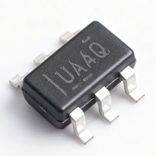
TS5A3159QDBVRQ1 - 1Ω SPDT Analog Switch AEC-Q100 | TI
The Texas Instruments TS5A3159QDBVRQ1 is an automotive-qualified (AEC-Q100) single-pole double-throw (SPDT) 2:1 analog switch with 1Ω typical ON-state resistance (1.3Ω max), operating from a 1.65V to 5.5V supply in a 6-pin SOT-23 (DBV) package. An analog switch is a semiconductor device that routes or gates analog and digital signals under the control of a logic-level input. Within the signal-chain hierarchy, the SPDT analog switch sits in the analog switches and multiplexers family, below large multiplexer arrays and alongside transmission-gate logic. An SPDT device connects one common (COM) terminal to either of two throw terminals (NO or NC), making it the fundamental building block of signal routing and redundancy switching. Key features include break-before-make switching, which prevents momentary channel shorting during transition and eliminates signal distortion when a signal source moves between paths; an excellent total harmonic distortion (THD) specification that preserves audio and precision-signal integrity; and low ON-resistance matching and flatness, which minimize signal error across the input range. The device operates from a single 1.65V to 5.5V supply, compatible with 1.8V, 2.5V, 3.3V, and 5V logic systems. The switch core uses a low-charge-injection MOS transmission-gate architecture with approximately 8pF typical ON capacitance (per TI family data), limiting high-frequency insertion loss in data and RF routing paths. The digital IN pin is logic compatible across the full supply range, and the -Q1 suffix denotes AEC-Q100 qualification with -40C to +125C operation for automotive environments. Typical applications include automotive audio source selection, sensor-signal multiplexing in battery-management and body-control modules, UART/SPI/SMBus line sharing, and general-purpose signal gating in industrial systems. The 2.9mm x 1.6mm SOT-23-6 footprint suits densely populated boards. Design tip: terminate or AC-ground unused throw terminals to reduce crosstalk, and place the device close to the signal source to minimize parasitic trace capacitance. This page synthesizes distributor pricing, drop-in alternatives, comparison tables, and practical design notes not found in the manufacturer datasheet.

TS5A63157 - 10-Ohm SPDT Analog Switch 1.65-5.5V | TI
The Texas Instruments TS5A63157 is a single-pole, double-throw (SPDT) analog switch, also described as a 2:1 multiplexer/demultiplexer, designed to operate from a 1.65 V to 5.5 V supply. It handles both digital and analog signals with a low on-state resistance of approximately 10-12 ohms and comes in a 6-pin SC-70 (SOT, SC70-6, DCK) surface-mount package. An analog switch is a type of signal-routing IC in the broader family of multiplexers and switches within the semiconductor component hierarchy. Unlike a relay or mechanical switch, an analog switch uses CMOS transmission gates to route signals with low distortion, fast switching times, and no moving parts, making it fundamental to signal-chain design in portable and battery-powered systems. Key features include overshoot and undershoot voltage protection: the device senses voltage events at the I/Os and responds by preventing voltage differentials from developing and turning the switch on. It also provides isolation in powered-off mode (leakage specified at 0 when V+ = 0), break-before-make switching, 5-V tolerant control inputs, low charge injection, and excellent on-state resistance flatness. Technically, the TS5A63157 uses a CMOS switch architecture with integrated protection circuitry, allowing it to survive I/O faults that would damage unprotected switches. The powered-off isolation makes it ideal for hot-swap and battery-powered systems where rails may be sequenced or removed while signal lines remain connected. Typical applications include battery-powered portable devices, audio signal routing, hot-swap USB and peripheral switching, and multiplexing sensor or test signals in instrumentation. Priced at roughly $0.34 in single units as of 2026-08-30 per distributor data, it is also cost-effective for high-volume designs. Design tip: ensure the control input logic level is compatible with the V+ rail; control inputs are 5-V tolerant regardless of supply, and the break-before-make timing prevents momentary shorting of the two switch paths during transitions.

TXB0104D - 4-Bit Bidirectional Level Translator, 100Mbps | TI
The Texas Instruments TXB0104D is a 4-bit bidirectional voltage-level translator with automatic direction sensing, delivering up to 100 Mbps data rates in a 14-pin SOIC (D) package, with VCCA from 1.2V to 3.6V and VCCB from 1.65V to 5.5V plus +/-15 kV ESD protection. A voltage-level translator (also called a level shifter) is a logic IC that interfaces digital circuits operating at different supply voltages, allowing a 1.8V microcontroller to safely communicate with a 3.3V or 5V peripheral. Level translators sit within the broader logic IC family, alongside buffers, transceivers, and bus switches, and are a fundamental part of system power-management and signal-chain design wherever mixed-voltage domains coexist. Key features of the TXB0104D include fully automatic direction sensing that eliminates the direction-control pin required by conventional transceivers, universal translation among 1.2V, 1.5V, 1.8V, 2.5V, 3.3V, and 5V nodes, and a 100 Mbps maximum data rate that supports fast embedded buses. An active-high OE input tri-states all eight I/Os when low, providing board-level power sequencing isolation. Architecturally, the TXB family uses two separate configurable power-supply rails: port A tracks VCCA and port B tracks VCCB. Internal one-shot circuits sense edges and briefly drive stronger pull-up/pull-down transistors, while a 4 kOhm series switch holds the level in static conditions. This push-pull CMOS design requires neither pull-up resistors nor direction control, but it does mean the TXB0104 is suited to push-pull CMOS outputs only, not open-drain buses unless replaced by the TXS family. Typical applications include MCU-to-peripheral interfacing across mixed voltage domains, SPI and UART signal translation, and general-purpose 1.2V-to-5V logic bridging in industrial and consumer systems. The -40C to +85C operating range covers most commercial and industrial environments. Design consideration: keep VCCA lower than or equal to VCCB, and remember the weak static drive (about 4 kOhm) cannot handle heavy loads, long wires, or pull-up resistors below about 50 kOhm. This page synthesizes verified distributor data, drop-in alternative analysis, and practical design notes not found in the manufacturer datasheet alone.
TXB0104RUTR - 4-Bit Bidirectional Level Shifter | Texas Instruments
The Texas Instruments TXB0104RUTR is a 4-bit bidirectional voltage-level translator with automatic direction sensing and ±15-kV ESD protection (Human Body Model), housed in a 12-pin UQFN (RUT) package measuring 1.7 mm x 2.0 mm. It translates signals between a low-voltage A port operating from 1.2 V to 3.6 V and a higher-voltage B port from 1.65 V to 5.5 V (VCCA <= VCCB), supporting data rates up to 100 Mbps. A voltage-level translator, also called a level shifter, is an integrated circuit in the logic-translation family that enables communication between digital devices operating at different supply voltages. In mixed-voltage systems, a 1.8 V or 3.3 V MCU may need to interface with 5 V peripherals; translators convert logic levels bidirectionally while protecting low-voltage silicon. The TXB0104 belongs to the auto-direction-sensing translator family, eliminating direction-control pins and simplifying both PCB design and firmware. Key features include per-channel automatic direction sensing, ±15-kV HBM ESD protection on all pins, tri-state outputs with an output-enable (OE) pin for bus isolation, and an operating temperature range of -40C to +85C. Low quiescent current and the tiny UQFN footprint suit space-constrained portable designs. Architecturally, the TXB0104 uses a one-shot edge accelerator that speeds rising and falling edges, enabling 100 Mbps operation with low static power. The A port tracks VCCA and the B port tracks VCCB. Partial power-down via OE and Ioff-style isolation make it suitable for hot-insertion environments. Typical applications include SPI, UART, and push-pull GPIO level shifting between MCUs, sensors, SIM card and SD card interfaces, and memory peripherals in mobile, industrial, and consumer products. The push-pull driver topology is not recommended for open-drain buses such as I2C or 1-Wire, as confirmed in TI E2E forum threads. Design tip: power VCCA before VCCB, place 0.1 uF bypass capacitors close to both supply pins, and use the OE pin for sequencing. For open-drain buses, consider TXS0104E instead.

TXB0104W-Q1 - 4-Bit Auto-Direction Level Translator | Texas Instruments
The Texas Instruments TXB0104W-Q1 is an automotive-grade 4-bit bidirectional voltage-level translator with automatic direction sensing, rated for data rates up to 100 Mbps and protected by +/-15 kV IEC ESD protection on the I/O pins, housed in a 12-pin UQFN (RUT) package. Qualified per AEC-Q100 for automotive applications, the W variant supports a VCCA supply range of 1.1 V to 3.6 V and a VCCB range up to 3.6 V, translating between logic families such as 1.2 V, 1.8 V, 2.5 V, and 3.3 V rails. A voltage-level translator is a member of the logic IC family (voltage-level translator -> logic IC -> integrated circuit) that allows two circuit domains operating at different supply voltages to exchange digital signals safely. On mixed-voltage PCBs - for example, a 1.8 V microcontroller talking to a 3.3 V sensor - the translator isolates the rails while preserving logic polarity and timing, preventing overvoltage damage and logic-level misreads. Key features of the TXB0104W-Q1 include automatic direction sensing that eliminates DIR control pins, push-pull topology optimization delivering 100 Mbps throughput, and a compact 12-pin UQFN footprint of approximately 2 mm x 2 mm that saves board area. The +/-15 kV ESD rating (IEC) on the I/O ports adds robustness in harsh automotive electrical environments. According to TI product data, the device uses two separate configurable power-supply rails; the A port tracks VCCA and the B port tracks VCCB. Architecturally, the TXB family uses a two-transistor output driver with an integrated one-shot edge-rate accelerator on each side, giving fast transition times for push-pull CMOS signals. This makes it well suited to SPI, UART, and general-purpose push-pull GPIO translation. Note that, as TI applications guidance states, the TXB architecture is not recommended for open-drain buses such as I2C or 1-Wire, where the internal drivers contend with external pull-ups. Typical applications include automotive body electronics and gateways translating between 1.8 V SoC GPIO and 3.3 V peripherals, infotainment and display module signal interfaces, and industrial control modules requiring AEC-Q100 qualified components. Design tip: keep VCCA ramps before or after VCCB within datasheet sequencing guidance, and place the two 0.1 uF decoupling capacitors directly at the VCCA and VCCB pins; the auto-direction sensing requires push-pull sources on both sides to function reliably. This page synthesizes distributor pricing tiers, verified drop-in alternatives from TI cross-reference discussions, and practical design notes not found in the manufacturer datasheet.
TXB0104YZTR - 4-Bit Auto-Direction Level Translator | TI
The Texas Instruments TXB0104YZTR is a 4-bit bidirectional voltage-level translator with automatic direction sensing, supporting 1.2V to 3.6V on the A port and 1.65V to 5.5V on the B port at data rates up to 100 Mbps, housed in a 12-ball DSBGA (YZT) package measuring 1.9 mm x 1.4 mm with +/-15 kV ESD protection. A voltage-level translator is a logic-interface device that allows integrated circuits operating at different supply voltages - for example a 1.8V microcontroller and a 5V sensor - to exchange digital signals reliably. Within the power-management and interface hierarchy, level translators sit between logic families such as CMOS and TTL, complementing buffers, bus switches, and transceivers in the broader signal-chain category. Without translation, low-voltage logic can be damaged by higher-voltage inputs or fail to meet higher-voltage logic thresholds. Key features of the TXB0104 include its two separate configurable power-supply rails (VCCA tracks the A port, VCCB tracks the B port, with VCCA <= VCCB), auto-direction sensing that eliminates direction-control pins, a maximum propagation delay of 13.7 ns, and 4 kV (HBM) class robustness supplemented by +/-15 kV IEC ESD protection on the I/O lines. The TXB architecture uses a mixed-charge pump output driver that pushes data in either direction without OE-based handshaking. Technically, the device derives its drive from a 4 kOhm output stage optimized for lightly loaded, point-to-point CMOS links; it is not a bus-holder for heavily capacitive or high-fanout loads. The 0.5 mm ball pitch and wafer-scale DSBGA packaging minimize board area, making it attractive for dense portable designs. The output enable (OE) pin tri-states all channels for power-aware sequencing. Typical applications include translating I2C-adjacent push-pull buses, SPI and UART links between 1.8V MCUs and 3.3V or 5V peripherals, SD-card interfaces, and general-purpose GPIO bridging in industrial and consumer systems. A key design consideration: avoid capacitive loads above roughly 30 pF and pull-up/pull-down resistors below about 25 kOhm, because the auto-direction scheme relies on one side driving the line; contested drivers cause bus contention. This page synthesizes distributor pricing, verified specifications, and practical design guidance for the TXB0104YZTR beyond what any single datasheet page provides.

TXB0108PWR - 8-Bit Bidirectional Level Shifter 100Mbps | TI
The Texas Instruments TXB0108PWR is an 8-bit bidirectional voltage-level translator with auto-direction sensing and +/-15-kV ESD protection, housed in a 20-pin TSSOP (PW) package. It translates signals between a 1.2V to 3.6V A port and a 1.65V to 5.5V B port (VCCA <= VCCB), with data rates up to 100 Mbps, making it ideal for mixed-voltage digital systems. A voltage-level translator is a logic IC that enables communication between devices operating at different supply voltages, such as a 1.8V microcontroller and a 3.3V or 5V peripheral. It sits in the hierarchy of logic ICs under level shifters (translators), which are essential in multi-voltage digital systems alongside buffers and bus transceivers. The TXB0108PWR uses auto-direction sensing, eliminating the need for a direction control pin and reducing firmware complexity. Key features include auto-direction sensing, +/-15-kV ESD protection (HBM), a 100 Mbps maximum data rate, and a VCC isolation feature: if either VCC input is at GND, all outputs enter the high-impedance state, enabling partial-power-down operation with Ioff support. The device operates from -40C to +85C. Technically, the TXB0108 uses a one-shot architecture that accelerates low-to-high transitions to achieve 100 Mbps. It is designed for push-pull (totem-pole) CMOS drivers only; for open-drain buses such as I2C, TI recommends the TXS0108E. Output drive is intentionally weak (internal 4 kOhm series resistors), so heavy capacitive loads above ~70 pF reduce achievable speed. Typical applications include 1.8V-to-3.3V microcontroller-to-sensor interfaces, SD card level shifting, UART/SPI signal translation, and FPGA configuration buses. The 100 Mbps capability suits high-speed SPI and UART links. Design tip: ensure VCCA <= VCCB, drive all eight channels push-pull, and place 0.1uF decoupling capacitors close to both VCCA and VCCB pins with short traces for signal integrity.