LED et optoélectronique
Sous-catégories
Produits (74)

TLD1211SJFUMA1 - 85mA Linear LED Driver, 28V max | Infineon
The Infineon TLD1211SJFUMA1 is an integrated adjustable constant-current LED driver IC fabricated in bipolar technology, delivering up to 85 mA to a single output stage with PWM dimming capability in an 8-pin PG-DSO-8-16 surface-mount package. It is part of the LITIX Linear family designed for severe automotive lighting environments, providing constant LED brightness over the full automotive supply range. A linear LED driver is a regulator topology that places a power device in series with the LED string, dropping excess supply voltage as heat while precisely regulating the current flowing through the LED load. Unlike switching LED drivers, linear drivers introduce no EMI and no switching ripple, simplifying PCB layout for noise-sensitive environments such as rear combination lamps and interior ambient lighting. Key features include a wide supply operating range of 5.5 V to 28 V (load-dump tolerant to 40 V), an external sense resistor that programs output current from a few mA up to 85 mA, integrated PWM dimming via the EN pin (accepting CMOS/TTL levels), and protection circuitry against over-temperature, over-current, and reverse polarity conditions typical of automotive 12V/24V bus systems. The TLD1211SJ uses a bipolar transistor process combined with a precision bandgap reference to set the sense voltage across the external resistor. Its low headroom requirement (typical Vsense around 0.5 V to 1.3 V at low current) minimizes wasted power while keeping the LED current tightly regulated across temperature and supply variations. Typical applications include automotive tail/brake lighting, turn indicators, daytime running lights (DRL), and interior LED strings where PWM dimming is required. The single-channel architecture suits single-LED or short-string loads where high efficiency is unnecessary but EMI-free operation and small PCB footprint matter. When designing with this part, ensure the PCB dissipates the (VIN - VLED) x IOUT heat via copper pour. Use a 1 percent or better external sense resistor (typically 13 ohm for 65 mA) for stable current matching across the automotive temperature range. This page synthesizes distributor pricing, drop-in alternatives, and practical automotive design notes not found in the Infineon datasheet alone, helping engineers select and validate the TLD1211SJFUMA1 against modern automotive LED lighting requirements.

TLP127(TPL,U,F) - 2500Vrms Darlington Optocoupler SO6 | Toshiba
The Toshiba TLP127(TPL,U,F) is a single-channel Darlington-output optocoupler housed in a 4-pin MFSOP6 (Mini-Flat SO6) surface-mount package, providing 2500 Vrms galvanic isolation between a GaAs infrared LED input and a silicon photodarlington output. The device delivers a minimum current transfer ratio (CTR) of 1000 % at IF=10 mA / VCE=2 V and supports a collector-emitter voltage of 300 V, a collector current of 150 mA, and a peak collector surge of 150 mA, making it well suited for programmable controller DC-output modules and telecommunication line interfaces. An optocoupler (also called an optoisolator or photocoupler) is a semiconductor device that transmits an electrical signal between two isolated circuits by using an internal LED-phototransistor optical link. The optocoupler category sits inside the broader optoisolator family, which in turn belongs to the signal-conditioning and isolation segment of the power management and interface IC tree. Darlington-output variants such as the TLP127 use a cascaded phototransistor pair to multiply the photo-induced base current, producing very high CTR and eliminating the need for an external driver stage in low-current interfaces. Key specifications include an isolation voltage of 2500 Vrms, a maximum collector-emitter voltage VCEO of 300 V, an on-state collector current of up to 150 mA, a forward voltage of 1.15 V at IF=10 mA, and a saturation voltage of 1.2 V at IC=100 mA. Switching characteristics are 15 us turn-on and 40 us turn-off measured at IF=10 mA, RL=100 ohm, which is acceptable for relay drivers and DC-output modules where sub-millisecond response is sufficient. The Darlington architecture combines two bipolar transistors on the receiver die, giving the TLP127 roughly 100x the current gain of a standard phototransistor optocoupler. This lets a 5 mA LED current drive a relay coil that would otherwise require a separate pre-driver, simplifying the BOM. The wide VCEO of 300 V also makes the part useful for 24 V and 48 V industrial buses, and the 2500 Vrms isolation meets IEC 60747-5-5 reinforced insulation requirements for industrial control equipment. Typical applications include programmable controller DC-output modules, telecommunication line interfaces, solid-state relay drivers, interface modules for measurement equipment, and battery-monitoring isolation in industrial automation. The combination of high CTR and high VCEO enables direct switching of 24 V relays without an external transistor, reducing board area. When designing with the TLP127, place the input-side current-limiting resistor to set IF between 5 mA and 20 mA and use a flyback diode across inductive loads. The 4-pin SO6 footprint is smaller than a DIP-6 optocoupler, so PCB layout must respect the minimum 5 mm creepage to preserve the rated isolation voltage. This page synthesizes distributor pricing, drop-in pin-compatible alternatives, and practical design guidance not collected in the Toshiba datasheet PDF, helping engineers select and qualify the TLP127(TPL,U,F) for new designs and second-source replacements.

TLP182(GR-TPL,E - AC Input Phototransistor Optocoupler, 3750Vrms | Toshiba
The Toshiba TLP182(GR-TPL,E is a low AC-input photocoupler consisting of a phototransistor optically coupled to two antiparallel InGaAs infrared emitting diodes, housed in a 6-pin SO6 (4-lead) surface-mount package. The device features a guaranteed 3750 Vrms isolation voltage, a collector-emitter breakdown voltage of 80 V minimum, and an operating temperature range of -55C to +125C, making it suitable for high-density industrial designs. The (GR) suffix denotes the Current Transfer Ratio (CTR) rank of 100% to 300% at IF = 5 mA and VCE = 5 V, while (TPL,E) specifies L-direction tape-and-reel packaging and RoHS compliance. A photocoupler (also called an optocoupler or opto-isolator) is a semiconductor device that transmits electrical signals between two isolated circuits using light. The category hierarchy is optocoupler > isolator > signal conditioning IC > semiconductor. Phototransistor-output optocouplers provide galvanic isolation while preserving analog or digital signal integrity, and are widely used to protect low-voltage logic from high-voltage transients on industrial buses, motor drives, and switching power supply feedback paths. The TLP182's antiparallel LED configuration enables direct AC input operation without polarity constraints, simplifying half-wave and full-wave rectified control interfaces. Key features of the TLP182 include 3750 Vrms isolation voltage, 50% minimum CTR at low IF = +/-0.5 mA (enabling high-efficiency LED drive), 80 V VCEO, and wide -55C to +125C operating range. The 4-lead SO6 package measures approximately 3.7 mm x 7.0 mm x 2.1 mm, providing high isolation in a compact footprint suitable for dense PCB layouts. The InGaAs infrared LED delivers faster switching characteristics compared with traditional GaAs emitters, supporting higher data rates in digital isolation applications. The TLP182 uses a double-molded optical coupling path between the input LED stack and the output phototransistor, achieving reinforced insulation per industry standards. The antiparallel LED arrangement means the device conducts on either half-cycle of an AC input, eliminating the need for a rectifier bridge in low-frequency AC sensing circuits. The SO6 package provides 5.0 mm minimum external creepage and clearance distances, supporting 250 V working voltage per IEC 60747-5-5. Typical applications include programmable logic controller (PLC) I/O modules, switching power supply feedback loops, AC line voltage sensing interfaces, communication interface isolation, hybrid IC signal transfer, and industrial control input modules. The wide temperature range and high CTR at low current make the TLP182 particularly well-suited for energy-efficient designs where LED drive current must be minimized. When designing with the TLP182, observe proper creepage and clearance distances on the PCB and ensure input-side current-limiting resistors match the chosen IF (typically 5-20 mA). The base pin is internally connected only on selected variants - on the standard TLP182 the base is left open, and external bias should not be applied unless confirmed against the specific datasheet variant. Always derate CTR at elevated temperatures per the datasheet curves. This page synthesizes distributor pricing, verified drop-in alternatives from Toshiba and competitor optocouplers, and practical design guidance not collected on any single manufacturer or distributor page.
TLP182GB-TPL.E - 3750Vrms AC-Input Phototransistor Optocoupler | Toshiba
The Toshiba TLP182GB-TPL.E is a 4-pin SO6 phototransistor-output optocoupler with 3750 Vrms isolation voltage, AC input capability, and an operating temperature range of -55°C to +125°C. The device consists of two antiparallel infrared LEDs optically coupled to a phototransistor, enabling direct AC-input drive without external rectification. Housed in a compact 6-SOP package (4 effective pins plus 2 NC), it targets high-density surface-mount applications where board real estate and isolation are critical. The GB-TPL.E suffix defines tape-and-reel packaging with a 125°C upper temperature rating. A photocoupler (also called an optoisolator) is a semiconductor device that transmits electrical signals between two isolated circuits using infrared light. Phototransistor-output optocouplers sit within the broader optocoupler family (which also includes triac, MOSFET, and Darlington outputs) and are commonly used for digital signal isolation in industrial control, switch-mode power supply feedback, and communication interfaces. The TLP182's AC-input design—achieved by antiparallel LED orientation—eliminates the need for input rectification, simplifying drive circuitry and reducing BOM count in PLC and AC-line-sensing applications. Key specifications include 3750 Vrms isolation voltage (per UL/VDE standards), 50 mA collector current maximum, 80 V collector-emitter voltage, and a current transfer ratio (CTR) characteristic that varies with part grade. The TLP182 is supplied in seven CTR grades (e.g., GB rank denoting 100% to 600% CTR), allowing designers to optimize sensitivity and switching speed for specific load conditions. The wide -55°C to +125°C operating range supports harsh-environment deployment. Architecturally, the TLP182 integrates a high-emitter-efficiency GaAlAs or GaAs LED pair with a silicon phototransistor receiver, isolated by a transparent silicone dielectric. The antiparallel LED arrangement accepts either polarity of AC input, while the phototransistor collector remains accessible as a single-ended output, simplifying biasing with a pull-up resistor to VCC. Typical applications include programmable logic controller (PLC) digital input modules, switching-mode power supply feedback loops, communication interface isolation, AC line-voltage sensing, and hybrid IC interface boards. The SO6 footprint suits high-density SMT assembly and reflow soldering. When designing with the TLP182, place a base-emitter resistor (typically 1-10 MΩ) across the phototransistor to reduce off-state leakage and improve switching speed. Ensure that the input LED drive current respects the absolute maximum ratings and that the supply voltage at the collector does not exceed VCEO. For switching-speed-sensitive designs, use a smaller pull-up resistor to accelerate the output rise time. This page synthesizes distributor pricing, drop-in alternatives, and practical design considerations not consolidated in the manufacturer datasheet alone.
TLP182GB-TPL.E(T - 3750Vrms AC Input Phototransistor Optocoupler | Toshiba
The Toshiba TLP182GB-TPL.E(T is a low AC-input type optocoupler consisting of a phototransistor optically coupled to two antiparallel infrared LEDs in a compact 4-pin SO6 package. The device provides 3750 Vrms minimum isolation voltage between input and output, a wide operating temperature range of -55 degC to +125 degC, and 50 mA collector current capability per the Toshiba datasheet. What is a phototransistor optocoupler? A phototransistor optocoupler (also called a photocoupler or optoisolator) is a semiconductor isolation device that transfers electrical signals between two isolated circuits using a light path. The category hierarchy is: optocoupler -> solid-state isolator -> isolation device -> semiconductor. AC-input types like the TLP182 use two antiparallel LEDs so that both halves of an AC waveform can drive the input, eliminating the need for an external rectifier bridge and simplifying AC line sensing applications. Key features include a collector-emitter voltage rating of 80 V, current transfer ratio (CTR) of 50% minimum at IF = 5 mA, VCE(sat) of 300 mV at IC = 2.4 mA / IF = 8 mA, and switching times of 2 us (ton) and 3 us (toff). The 4-lead SO6 surface-mount package supports high-density PCB assembly, and the device is supplied on tape-and-reel for automated production lines. The TLP182 architecture uses two antiparallel GaAs infrared LEDs, an optically transparent isolation gap, and a silicon NPN phototransistor. This configuration allows bidirectional AC triggering while preserving galvanic isolation, preventing ground loops and protecting downstream logic from high-voltage transients on the input side. The 3750 Vrms rating complies with IEC 60747-5-2-style reinforced isolation for industrial voltage levels. Typical applications include communication interface isolation, PLC (programmable logic controller) input modules, switching power supply feedback loops, hybrid IC signal paths, and AC line-voltage sensing. The wide temperature range makes the device suitable for industrial and automotive-grade environments requiring reliable operation across extreme conditions. When designing with this device, derate CTR for high-temperature operation (CTR drops roughly 30% from 25 degC to 100 degC) and provide a base-emitter resistor if low-dark-current operation is required. The 6-pin package only uses 4 leads, leaving pins 5 and 6 available for mechanical stability and PCB routing convenience. This page consolidates distributor stock, parametric drop-in alternatives, and practical PCB layout guidance not present in the manufacturer datasheet, helping engineers shorten component selection time.

TLP182GR - 3750Vrms AC Input Photocoupler | Toshiba SO6
The Toshiba TLP182GR is a low AC-input phototransistor optocoupler housed in a 6-pin SO6 (4-pin SO6) surface-mount package, providing 3750 Vrms of galvanic isolation between input and output. It integrates two antiparallel infrared LEDs that allow direct AC or bidirectional DC drive on the input side, simplifying logic-level interfacing without polarity constraints. The device delivers a minimum current transfer ratio (CTR) of 100% at IF=5mA, VCE=5V (GR rank), making it well-suited for digital signal isolation and slow-speed analog sampling. An optocoupler (also called optoisolator or photocoupler) is a semiconductor isolation device combining an infrared emitter LED and a photodetector inside a single hermetic package. Light, not electrical current, transmits the signal across an isolation barrier, achieving galvanic isolation rated in volts (often kVrms). Phototransistor-output optocouplers like the TLP182 sit in the hierarchy of solid-state relays -> optoisolators -> isolators -> signal-conditioning ICs. They are favored over transformer or capacitor isolation when extremely low propagation delay is not required but cost-effectiveness, bidirectional AC input, and high isolation voltage matter. Key features of the TLP182 include 3750 Vrms isolation voltage, an operating temperature range of -55C to +125C, collector-emitter voltage of 80V, and a typical propagation delay of a few microseconds. The GR rank bin guarantees CTR between 100% and 300% at IF=5mA, VCE=5V, with other ranks (GB, BL) offering different CTR windows. The SO6 footprint is industry-standard, simplifying layout on multi-channel PLCs and interface boards. The TLP182 uses a high-speed infrared GaAs LED coupled to a silicon phototransistor through a transparent dielectric isolation barrier. The antiparallel LED arrangement allows both polarities of input current to produce light, supporting AC-line or polarity-agnostic DC switching. The high CTR at low IF reduces drive-current requirements on microcontroller GPIOs. Typical applications include PLC digital input modules, AC-line detection interfaces, communication interface isolation, programmable logic controller signal isolation, and power-supply feedback loops where the primary-side error amplifier must be isolated from the secondary-side PWM controller. Its wide operating temperature also makes it attractive for industrial and factory-automation equipment. When designing with the TLP182, ensure the input current IF is kept above the CTR bin threshold (typically >=1mA to 5mA) and below the absolute maximum of 50mA. Add a base-emitter resistor across the phototransistor to improve switching speed and reduce leakage-induced false triggers, and provide adequate creepage/clearance on the PCB between primary and secondary copper pours. This page consolidates distributor pricing, parametric drop-in alternatives, and design guidance not found in a single datasheet, helping engineers evaluate sourcing options and PCB-ready substitutes for the TLP182GR.
TLP183(GB-TPL - Phototransistor Optocoupler, 3750Vrms, 6-SO | Toshiba
The Toshiba TLP183(GB-TPL is a low-input-current phototransistor optocoupler housed in a compact 4-pin SO6 surface-mount package, providing 3750 Vrms galvanic isolation between input and output. It consists of an InGaAs infrared emitting diode optically coupled to a silicon phototransistor, configured as a single-channel device with one emitter and one collector/detector pair on the secondary side. The GB CTR (Current Transfer Ratio) rank guarantees a defined transfer characteristic band, which simplifies design-in for DC input applications. A photocoupler (also called an optoisolator or opto) is a semiconductor isolation device that transfers an electrical signal between two circuits using a light-emitting element on the input side and a light-sensitive element on the output side, separated by a transparent insulating barrier. Photocouplers sit hierarchically under optoisolators -> isolation devices -> signal conditioning -> semiconductors. They are essential where safety regulations (UL, IEC 60747-5-5, VDE) require reinforced isolation between a hazardous high-voltage domain and a user-accessible low-voltage domain such as a microcontroller or logic IC. The TLP183 belongs specifically to the phototransistor-output subfamily, where the output stage is a BJT rather than a logic gate, TRIAC, or MOSFET - making it a general-purpose analog/digital signal isolator. Key specifications include: minimum 50% current transfer ratio (CTR, IF=5 mA, VCE=5 V), 80 V collector-emitter breakdown voltage (VCEO), 6 V reverse voltage on the input LED, and 50 mA forward current capability. The device supports a wide operating temperature range from -55 C to +125 C, exceeds most competitor parts that top out at -40 C, and provides 3750 Vrms isolation voltage per UL 1577 / IEC 60747-5-5 standards. Switching characteristics are specified with ton/toff on the order of a few microseconds, making it suitable for digital logic isolation, feedback paths in switching power supplies, and ground-loop isolation in industrial interfaces. From an architectural standpoint, the TLP183 is optimized for low-input-current operation: it can be driven from 1 mA to 20 mA forward current, which means a logic-level GPIO with appropriate series resistor can directly modulate the input LED. The phototransistor output allows the designer to choose pull-up voltage from VCEO down to logic levels, enabling level translation between domains running at different voltages (e.g., 3.3 V microcontroller to 5 V peripheral, or 5 V logic to 24 V PLC input). Typical applications include PLC input/output isolation, communication interface isolation (RS-232/RS-485 driver-receiver isolation, CAN bus isolation), AC adapter feedback paths, programmable controller interfaces, and I/O interface boards. The small SO6 footprint allows high-density surface-mount assembly, replacing larger DIP-package optocouplers without PCB redesign. Compared to logic-output optocouplers (such as Toshiba TLP2761 or TLP2361), the TLP183 provides a linear analog output rather than a hard-switched digital output, which is required in feedback loops and analog signal isolation. When designing with this part, size the input resistor so that IF stays between 1 mA (for low-current logic driving) and 20 mA (the absolute maximum). For a 5 V GPIO with Vf of 1.2 V, a 1.5 kOhm to 3.3 kOhm resistor yields 1.2-2.5 mA - within the GB CTR rank operating range. Add a base-emitter resistor (typically 100 kOhm to 1 MOhm) on the phototransistor to improve switching speed by reducing the Miller-effect charge storage. Provide adequate creepage and clearance per the PCB layout guideline in the manufacturer datasheet to maintain 3750 Vrms isolation in production. This page synthesizes distributor pricing, drop-in alternatives from the same Toshiba optocoupler family, and practical design notes not found in the standalone datasheet, providing a one-stop engineering reference for component selection.
TLP183(GB-TPL,E - 3750Vrms Phototransistor Optocoupler SO6 | Toshiba
The Toshiba TLP183(GB-TPL,E is a low-input-current phototransistor optocoupler housed in a compact 4-lead SO6 (SOIC-6 equivalent, 6-SOP) surface-mount package, providing 3750 Vrms of galvanic isolation between input and output. It integrates a GaAs infrared LED optically coupled to a phototransistor in a black ceramic-reinforced molding compound, and is qualified for operation across the -55°C to +125°C industrial temperature range. The GB current-transfer-ratio (CTR) rank is specified at 100% to 600% at IF=5 mA, VCE=5 V, distinguishing it from lower- and higher-rank siblings in the same family. An optocoupler (also called an optoisolator or photocoupler) is a semiconductor device that transmits electrical signals between two isolated circuits using a short optical transmission path. The phototransistor-output topology - the dominant sub-type of optocoupler - uses a silicon phototransistor as the receiving element, offering higher load-current handling than logic-output counterparts (e.g. TLP2361) and supporting AC-coupled or DC-coupled analog signal isolation. Within the broader isolation taxonomy (optical isolation -> galvanic isolation -> circuit isolation -> signal conditioning), optocouplers sit alongside digital isolators (capacitive, inductive) as a foundational circuit-protection element in PLCs, motor drivers, switch-mode power supply feedback loops, and communication-interface cards. Key differentiating specifications include 3750 Vrms minimum isolation voltage (per UL 1577), a collector-emitter voltage (VCEO) rating of 80 V, and a collector current (IC) capability of 50 mA. The CTR rank 'GB' defines the IF=5 mA current transfer ratio between 100% and 600%, distinguishing it from the GR rank (100%-300%) and BL rank (200%-600%). The device is supplied in tape-and-reel packaging (TPL suffix) with embossed taping, optimized for high-density surface-mount assembly lines. Architecturally, the TLP183 uses a GaAs infrared emitting diode (λp ≈ 940 nm) coupled through a transparent silicone optical bond to a silicon NPN phototransistor. The pair is mounted in opposing lead-frame cavities separated by a transparent insulating barrier, delivering both high common-mode transient immunity (CMTI) and creepage/clearance distances that meet 3750 Vrms reinforced-insulation requirements in most pollution-degree-2 industrial environments. Typical applications include PLC digital input modules, AC adapter feedback loops, I/O interface boards, programmable-controller signal conditioning, and office-machine interface isolation. The wide operating temperature range also supports outdoor and industrial-automation equipment. This part is the GB-rank variant; the GR, BL, and blank-rank variants of the same TLP183 family share the footprint but offer different CTR windows for different bias-point designs. When designing with the TLP183, observe the absolute-maximum IF of 50 mA through the input LED and the absolute-maximum VCEO of 80 V at the transistor output. A base-emitter resistor of approximately 1 MΩ is recommended across the B-E junction to improve high-temperature dark-current behavior, and a 100 kΩ pull-up on the collector is typical for digital-logic interfacing. This page consolidates distributor pricing, same-package drop-in equivalents such as TLP182 and TLP185, and practical PCB-layout notes not duplicated in the manufacturer datasheet.

TLP183(GB-TPL.E(T - Phototransistor Optocoupler | Toshiba
The Toshiba TLP183(GB-TPL.E(T is a low-input-current phototransistor output optocoupler featuring a GaAs infrared LED optically coupled to a phototransistor, housed in a 4-pin SO6 (mini-flat) surface mount package. It provides 3750 Vrms of galvanic isolation between input and output, a current transfer ratio (CTR) range of 100% to 600% (GB rank), and wide operating temperature support from -55 °C to +125 °C. The part is supplied on tape-and-reel (TPL) and carries the (E designation for compliance with RoHS requirements. An optocoupler (also called an opto-isolator or photocoupler) is a semiconductor device that transmits an electrical signal between two isolated circuits using a short optical transmission path through an optically transparent insulating barrier. The hierarchy is: optocoupler -> isolator -> solid-state relay family -> discrete semiconductor. Optocouplers are essential where ground loops, high-voltage transients, or safety isolation barriers must be crossed without a galvanic (conductive) path; the TLP183 family is widely used in industrial PLCs, communication interfaces, switch-mode power supply feedback loops, and I/O modules. Key features include a forward current IF of 5 mA typical (low-input drive), a collector-emitter voltage VCEO of 80 V, a current transfer ratio (CTR) of 100-600% at IF=5 mA and VCE=5 V, and a response time tr/tr of approximately 4 microseconds. The 4-pin SO6 package is roughly one-third the footprint of a DIP-4 optocoupler, making this part well-suited to high-density surface-mount designs where a smaller isolation device is required. The TLP183 employs a GaAs infrared LED (peak wavelength ~940 nm) bonded to a silicon NPN phototransistor in a reflective optical cavity. The high BVCEO rating of 80 V supports switching of higher-voltage rails than typical 30 V or 60 V optocouplers, and the low-input-current design reduces driver power consumption in MCU-driven interfaces. Typical applications include PLC input modules, communication-interface signal isolation, switch-mode power supply (SMPS) feedback paths, programmable controller digital I/O, and AC adapter ground-loop isolation. The 3750 Vrms rating satisfies most reinforced-isolation requirements for industrial low-voltage control circuits. When designing with this part, place at least 1 mm of creepage clearance around the package body to preserve the isolation rating; the SO6 outline requires it for 230 V AC mains-reinforced designs. A base-emitter resistor (~100 kΩ across B-E) on the phototransistor improves switching speed at the cost of slightly lower CTR. This page synthesizes distributor pricing, drop-in alternative cross-references, application circuits, and practical design notes that go beyond the Toshiba datasheet alone.
TLP183(GB-TPLE(T - 3750Vrms Phototransistor Optocoupler SO6 | Toshiba
The Toshiba TLP183(GB-TPLE(T is a low-input-current phototransistor optocoupler housed in the SO6 (4-pin SO6) surface-mount package, delivering 3750 Vrms isolation and a wide operating temperature range of -55 °C to +125 °C. The device pairs a GaAs infrared LED with a phototransistor detector to provide logic-level signal transfer across an reinforced galvanic isolation barrier, and is qualified to the GB current-transfer-ratio bin (CTR typically 100% minimum at IF = 5 mA, VCE = 5 V) per Toshiba binning convention. An optocoupler (also called a photocoupler or opto-isolator) is a semiconductor device that transmits electrical signals between two isolated circuits using light. The architecture is LED -> dielectric isolation barrier -> photodetector, which converts input current into infrared photons that traverse an electrically-non-conductive polymer or air gap before being re-converted to a current on the output side. This provides galvanic isolation rated in volts (here 3750 Vrms), preventing high-voltage transients, ground loops, and common-mode noise from coupling between the primary and secondary circuits. Phototransistor-output optocouplers such as the TLP183 belong to the broader isolator/solid-state-relay family, sit hierarchically under transistors and optocouplers, and are commonly used to bridge low-voltage digital logic with industrial 24 V or 230 V AC domains. Key features of the TLP183 include a collector-emitter breakdown voltage VCEO of 80 V (min), current transfer ratio (CTR) graded into GB/GR/H bins for design flexibility, an input forward current IF max of 50 mA, and a low typical forward voltage VF of approximately 1.25 V at 10 mA. The SO6 (4 effective pins) package provides a minimum creepage distance suitable for reinforced insulation in industrial control equipment, while the surface-mount form factor is significantly smaller than legacy DIP-4 optocouplers. The TLP183 architecture uses a high-efficiency GaAs infrared LED emitter optically coupled to a silicon NPN phototransistor, with the GB CTR bin targeting the 100%-to-300% range at IF = 5 mA, VCE = 5 V. This makes the part well suited for low-input-current applications where the driving side has limited source current, such as microcontroller GPIO pins or battery-management interfaces. Compared with high-speed gate-driver optocouplers, the TLP183 is optimized for slower switching speeds (typical ton/tof in the microsecond range), trading bandwidth for robust CTR over temperature. Typical applications include PLC digital input modules, communication-interface isolation, switched-mode power supply (SMPS) feedback loops, industrial sensor interfaces, and home appliance control boards. The part's wide -55 °C to +125 °C operating range and 3750 Vrms isolation rating also suit factory-automation equipment and renewable-energy inverter control sections. When designing with the TLP183, ensure that the input-side current-limiting resistor is sized for the chosen CTR bin - a CTR of 100% at IF = 5 mA means the output transistor can sink approximately 5 mA at VCE = 5 V. Always observe maximum IF (50 mA) and power dissipation limits, and add a base-emitter resistor if slow turn-off is unacceptable in the target switching frequency. This page synthesizes distributor pricing, drop-in alternative listings, and practical design notes not found in the Toshiba datasheet, sourced from DigiKey, Mouser and TTI as of 2026-10-11.
TLP183(GR) - 3750Vrms Phototransistor Optocoupler, SO6 | Toshiba
The Toshiba TLP183(GR) is a 4-pin SO6-package phototransistor optocoupler that delivers 3750 Vrms isolation, 50% minimum current transfer ratio (CTR) at IF=0.5 mA, and an 80 V minimum collector-emitter breakdown voltage for DC input / transistor output isolation. It operates across -55C to +125C with a GaAs infrared LED optically coupled to a silicon phototransistor, packaged in a compact surface-mount SO6 outline. A phototransistor optocoupler (also called a photocoupler or optoisolator) is a semiconductor isolation component that transfers electrical signals between two circuits using a light path, providing galvanic isolation while allowing signal or low-power control coupling. Within the broader hierarchy, it belongs to: optocoupler -> isolator -> signal conditioning component -> discrete semiconductor, commonly classified under isolators/solid-state relays. Phototransistor output types are the workhorse of low-speed digital isolation in industrial, PLC, and power-supply feedback paths. Key features include 3750 Vrms minimum isolation voltage, 50% minimum CTR at IF=0.5 mA / VCE=5 V (GR bin grading), 80 V minimum VCEO, 6 V minimum VECO, 50 mA collector current capability, and 4 us typical switching speed. The SO6 footprint is significantly smaller than legacy DIP optocouplers, enabling high-density surface-mount designs on programmable controller and SMPS boards. Internally, the TLP183(GR) uses a GaAs infrared LED die facing a silicon NPN phototransistor die across an optically transparent isolation barrier. The GR CTR bin narrows the transfer-ratio window to 100-300% at IF=5 mA, simplifying design-in when a known gain band is required versus the broader TLP183 base spec. Typical applications include programmable logic controller (PLC) digital input isolation, switching power supply feedback loops, communication interface line receivers, and any high-density industrial control board needing logic-level signal isolation across a 3750 Vrms isolation barrier. When designing with this part, observe the IF=0.5 mA low-input drive condition that defines the minimum CTR - derate IF to keep the LED within its absolute maximum ratings, and provide a 0.1 uF bypass cap across the output collector supply when used in noisy industrial environments. This page synthesizes distributor pricing, drop-in alternatives, and practical design notes not found in the manufacturer datasheet, providing engineers with a single reference for sourcing and substituting the TLP183(GR) in new or legacy designs.
TLP183(GRH-TPLE - Phototransistor Optocoupler 3750Vrms SO6 | Toshiba
The Toshiba TLP183(GRH-TPLE is a low-input type phototransistor optocoupler in a 6-pin SO6 (SOIC-6 narrow body) surface-mount package, integrating an infrared LED optically coupled to a silicon phototransistor. Key parameters include a minimum collector-emitter voltage of 80 V, current transfer ratio (CTR) of 50% minimum at IF = 0.5 mA and VCE = 5 V, and isolation voltage of 3750 Vrms. The device operates over a wide temperature range of -55 °C to +125 °C. A phototransistor optocoupler is a type of optoisolator (also called photocoupler) that transfers electrical signals between two isolated circuits using light. The device consists of an infrared LED on the input side and a phototransistor on the output side, separated by a transparent dielectric barrier that provides galvanic isolation. This places the part in the broader hierarchy of optoisolator -> isolator -> interface IC -> semiconductor, where the SO6 narrow-body package family enables high-density surface-mount designs typical in industrial control and communication interface applications. Key features include a low-input current requirement of just 0.5 mA IF for the minimum CTR condition, making this part a low-input type suitable for direct connection to low-power logic or microcontroller outputs. The 3750 Vrms isolation withstand voltage meets common safety standards for reinforced isolation in industrial systems, and the 80 V VCEO rating supports higher-voltage analog and digital signal chains. The TLP183(GRH-TPLE uses a 4-pin SO6 footprint (also called SOIC-6 narrow body) that is the smallest available in the Toshiba TLP182/TLP183 series. The infrared LED is constructed using GaAs (gallium arsenide) technology, while the output phototransistor uses a standard silicon NPN process, providing proven reliability across millions of operating cycles typical of programmable logic controllers and communication interface applications. Typical applications include PLC input/output isolation, communication interface line drivers/receivers, power supply feedback loops requiring primary-to-secondary isolation, and digital logic isolation between mixed-voltage domains. Its compact SO6 footprint makes it suitable for high-density surface mounting. When designing with this device, ensure the input current IF is set within the recommended operating range (typically 0.5 mA to 25 mA) to guarantee the specified CTR. The output phototransistor requires a pull-up resistor on the collector; choose the value based on the desired switching speed and load voltage. This page synthesizes distributor pricing, same-package alternatives (TLP183 family variants), and practical design notes not found in the standalone manufacturer datasheet.
TLP183(TPL - 3750Vrms SO6 Phototransistor Optocoupler | Toshiba
The Toshiba TLP183(TPL is a low-input-current phototransistor optocoupler housed in the very small and thin SO6 (4-pin SO6 outline) surface-mount package. It integrates a GaAs infrared LED on the input side and an NPN silicon phototransistor on the output side, providing a guaranteed isolation voltage of 3750 Vrms and a wide operating temperature range of -55 C to +125 C. The TLP183 series is part of Toshiba's low-input-type coupler family, optimized for digital logic interfacing, programmable logic controllers, and power-supply feedback loops. A phototransistor optocoupler (also called a photocoupler or opto-isolator) is a semiconductor device that transfers electrical signals between two isolated circuits using a light beam inside a sealed package. The input LED converts an electrical current into infrared light, and the output phototransistor converts the light back into a current proportional to the received optical flux. Because there is no galvanic connection between input and output, the device provides galvanic isolation - the foundation of safety in PLC I/O modules, switching power supplies, industrial communication interfaces, and any application where high-voltage transients on one side must not reach sensitive low-voltage logic on the other side. Within the broader component taxonomy, phototransistor optocouplers sit under: optoisolator -> isolator -> solid-state relay precursor -> interface IC. The TLP183 distinguishes itself with a 3750 Vrms isolation voltage (per UL1577 / VDE 0884 expectations typical for the SO6 family), a current transfer ratio (CTR) of 50% minimum at IF = 5 mA, VCEO = 80 V collector-emitter breakdown, and a response time of approximately 4 us (ton/toff). The SO6 package is roughly one-third the footprint of a DIP-4 optocoupler, enabling reflow-compatible surface mounting at high density. Internally, the LED die emits at a peak wavelength near 940 nm, matched to the silicon phototransistor's peak responsivity band. The base of the phototransistor is typically pinned out internally to a no-connect or brought out depending on variant; TLP183 has the base NC by design, simplifying application circuits. CTR binning options (BL / GR / GB / Y / etc.) allow the designer to select the current transfer range that matches their biasing and switching-speed requirements. Typical applications include PLC digital input modules (24V signal isolation to 3.3V/5V logic), switching-mode power supply (SMPS) primary-to-secondary feedback (TL431-style isolation paths), communication interface isolation (RS-232/RS-485 line-side isolation), IGBT/MOSFET gate-drive signal isolation in motor drives, and AC-line zero-cross detection. When designing with the TLP183, ensure the LED forward current (IF) is biased within the 1-20 mA recommended range for stable CTR; do not exceed IF = 50 mA. A 10 kohm pull-up on the collector with a 5V logic rail typically works for 5V digital interfaces; for 3.3V logic, verify the dark-current and CTR minimums at your operating temperature. This page synthesizes distributor pricing, same-brand and cross-brand drop-in alternatives, and practical design notes not consolidated on the manufacturer product page.

TLP250(TP1,F) - 1.5A Isolated Gate Driver Optocoupler | Toshiba
The Toshiba TLP250(TP1,F) is an 8-pin DIP optocoupler gate driver that combines an infrared LED input with an integrated photo-IC output stage, delivering 1.5A peak output current and 2500Vrms of galvanic isolation in a through-hole PDIP-8 package. Designed specifically for driving the gates of power MOSFETs and IGBTs in switching power converters, the device features a totem-pole CMOS output capable of sinking and sourcing up to 1.5A to charge and discharge large gate capacitances quickly. An optocoupler (also called an opto-isolator) is a semiconductor device that transmits electrical signals between two circuits using a short optical path while providing complete electrical isolation. Gate-driver optocouplers such as the TLP250 sit within the broader hierarchy of isolators (optical -> magnetic -> capacitive), which itself belongs to the power-management semiconductor category. They are essential whenever a low-voltage controller must command a high-voltage power stage without any galvanic path between them, ensuring safety and preventing ground loops. Key features of the TLP250(TP1,F) include a propagation delay of approximately 0.5 us, a common-mode transient immunity (CMTI) suitable for fast switching edges, and a wide operating temperature range that supports industrial environments. Internally the device uses a GaAlAs infrared LED coupled to a high-speed photo-diode receiver followed by a driver stage, allowing it to operate from a wide supply range. The (TP1,F) suffix denotes tape-and-reel packaging with the standard lead-free, RoHS-compliant termination finish. Typical applications for the TLP250(TP1,F) include isolated gate drivers for IGBT modules in motor-control inverters, primary-side drivers for half-bridge and full-bridge switch-mode power supplies, solar inverters, induction-heating inverters, and any industrial application that requires reinforced isolation between the logic-level control side and the high-voltage power side. Its 1.5A peak output capability allows it to drive IGBTs rated up to several hundred amperes without an external buffer stage. Engineers commonly pair it with the ACPL-P343 or HCPL-3120 when a closer pin-compatible alternative is required. When designing with the TLP250, observe the bypass-capacitor recommendations in the manufacturer datasheet: a 0.1 uF ceramic capacitor placed as close as possible to pins 8 and 5 (VCC and GND) is required for stable output switching, and an input-side current-limiting resistor must be chosen so that the LED forward current lies within the recommended 7-10 mA range. Designers should also note that the TLP250(TP1,F) has reached end-of-life status; the Toshiba TLP250H(TP1,F) and Broadcom HCPL-3120-500E are the closest drop-in cross-references available today. This page synthesizes distributor pricing, lifecycle status, drop-in alternatives, and practical design considerations that are not consolidated on the manufacturer datasheet alone, enabling engineers to compare, source, and design confidently around this established gate-driver optocoupler.

TLP293-4 - 4-Ch 3750Vrms Transistor Optocoupler SO16 | Toshiba
The Toshiba TLP293-4 is a quad-channel phototransistor optocoupler featuring four independent InGaAs infrared LEDs optically coupled to four phototransistors in a compact SO16 surface-mount package, with 3750 Vrms isolation voltage and a wide operating temperature range of -55C to +125C. The device delivers a minimum Current Transfer Ratio (CTR) of 50% at IF=5 mA and VCE=5 V, typical response time tr/tf of 3 us, and isolation voltage rated at 3750 Vrms per UL 1577-equivalent testing. An optocoupler (also called optoisolator or photocoupler) is a semiconductor isolation device that transmits electrical signals between two isolated circuits using a light path. Internally, an input infrared LED converts the input current into modulated light; the receiving-side phototransistor converts that light back into a current. This optical galvanic isolation - rated at 3750 Vrms for the TLP293-4 - allows safe interfacing between high-voltage and low-voltage domains, eliminating ground loops and protecting low-voltage microcontrollers from transient voltage spikes. Optocouplers occupy the broader category hierarchy of isolator -> signal isolator -> digital isolator alternative (optical) -> semiconductor isolation device. Key features of the TLP293-4 include 4 independent channels in one SO16 package, 3750 Vrms isolation, -55C to +125C operating range, CTR of 50% minimum (GB rank), collector-emitter voltage VCEO of 80 V, and forward current IF up to 50 mA. The SO16 package provides 2.54 mm pin pitch and is compatible with high-density PCB layouts used in PLC and I/O interface boards. The TLP293-4 uses Toshiba's InGaAs infrared LED emitter and silicon phototransistor detector process. The high VCEO of 80 V enables the output stage to switch 24 V logic-level signals directly, simplifying interface to industrial PLC backplanes. Each channel's base pin is left unconnected internally, reducing parasitic coupling and improving common-mode transient immunity. Typical applications include programmable logic controller (PLC) input/output isolation, communication interface line receivers, switching power supply feedback loops, and industrial 24 V digital signal isolation. The SO16 footprint and 3750 Vrms rating make the TLP293-4 especially well-suited for multi-channel industrial modules where PCB real estate is at a premium. When designing with the TLP293-4, observe the CTR derating with temperature and forward current. Provide input current-limiting resistors sized for the desired IF (typically 5-20 mA), and add a pull-up resistor at the collector output. Ensure the supply decoupling capacitor is placed close to the VCC pin of the receiver circuit. This page synthesizes distributor pricing from DigiKey, Mouser, Arrow, and LCSC, real-time stock signals, 4-channel photocoupler drop-in alternatives, and practical PLC interface design notes not consolidated on the manufacturer datasheet.

TLP3083F - Zero-Cross Photo Triac 800V 5kVrms | Toshiba
The Toshiba TLP3083F is a zero-crossing phototriac optocoupler housed in a 6-pin DIP6 (F-type wide-creepage) package, integrating a GaAs infrared LED optically coupled to a photo-triac. The TLP3083F delivers a peak off-state repetitive voltage (VDRM) of 800 V and an isolation voltage of 5000 Vrms, while featuring a zero-voltage-crossing (ZVC) detector that eliminates EMI by switching the triac only near the AC mains zero crossing. The 6-DIP F-type wide-creepage footprint provides reinforced insulation thickness of 0.4 mm minimum, allowing designers to meet international safety standards on a single package outline. A phototriac optocoupler (also written phototriac coupler or zero-cross triac driver) is a type of solid-state relay (SSR) that combines an input-side infrared LED with an output-side photosensitive triac. The LED electrically isolates the low-voltage control circuit from the AC mains while transmitting a switching signal through an optical path. Compared with random-phase triac drivers, zero-crossing variants such as the TLP3083F substantially reduce electromagnetic interference and inrush current, making them ideal for resistive AC loads. The TLP3083F sits within the broader hierarchy of isolators > solid-state relays > optocouplers > phototriacs > semiconductor devices. Key features include a peak off-state voltage of 800 V (VDRM), an on-state RMS current rating that supports typical SSR output stages, a trigger LED forward current of approximately 10 mA, and a halogen-free DIP6 package option. The zero-crossing detection circuit prevents the output triac from firing while the line voltage is non-zero, which suppresses RFI spikes and protects downstream loads. Reinforced 0.4 mm insulation thickness ensures compliance with IEC 60747-5-2 reinforced-insulation creepage requirements when proper PCB clearance is maintained. Typical applications include solid-state relay (SSR) output stages, AC triac drivers for home appliances such as washing machines and air conditioners, office equipment switching, and industrial temperature controllers. Designers should observe the published trigger current limits and provide adequate PCB creepage distances to maintain the rated 5000 Vrms isolation. This page synthesizes distributor pricing, drop-in alternatives, and design notes that go beyond the manufacturer datasheet.
TLP590B - Photovoltaic Optocoupler, 7V/12µA, 2500Vrms, DIP-6
The Toshiba TLP590B is a photovoltaic-output optocoupler consisting of an aluminum gallium arsenide (AlGaAs) infrared emitting diode optically coupled to a photo-diode array, housed in a six-lead plastic DIP package. The TLP590B delivers an open-circuit output voltage VOC of 7V and a short-circuit current ISC of 12 µA, with a 2500 Vrms isolation voltage rating, making it well suited as a solid-state replacement for mechanical relays in low-power switching applications. What is a photovoltaic optocoupler? It is a type of optoisolator whose output stage is a series-connected photodiode array that generates a small DC voltage when the input LED is forward-biased. Unlike transistor-output optocouplers that require an external supply, photovoltaic couplers act as optically-driven DC voltage sources, sitting in the hierarchy: optoisolator > solid-state relay > photocoupler > photovoltaic coupler > signal isolation device. Key features of the TLP590B include a high open-circuit voltage that eliminates the need for separate driver ICs in low-power MOSFET gate drive circuits, an AlGaAs LED emitter for stable optical output, and a 6-DIP through-hole package (5 active leads, 1 cut) compatible with standard PCB footprints. The device supports MOS gate driver applications, programmable controllers, and telecommunication line interface circuits. Technically, the TLP590B relies on series-connected photodiodes that multiply the single-junction photovoltaic voltage (≈0.6V) to deliver 7V at the output terminals. The 12 µA short-circuit current capability is sufficient to directly drive small-signal MOSFET gates or to feed a discrete MOSFET gate-charge pump circuit without an auxiliary bias supply, which simplifies isolated DC-DC converter designs. Typical applications include MOSFET gate drivers in solid-state relays, programmable logic controller (PLC) input isolation, telecommunication line interface cards, and battery management systems (BMS) where the photocoupler provides reinforced isolation between high-voltage battery stacks and low-voltage monitoring MCUs. When designing with the TLP590B, ensure the LED forward current is set within the recommended operating range (typically IF = 10-20 mA) to achieve the rated VOC and ISC. For higher gate-drive currents, a buffer MOSFET is required since the 12 µA output is intended only for high-impedance gates. This page synthesizes distributor pricing, drop-in alternatives, and practical design notes not found on individual distributor listings, including verified same-brand Toshiba photovoltaic optocouplers in the same DIP-6 footprint for direct PCB-level substitution.
TLP590B(C.F) - 7V/12uA Photovoltaic Optocoupler, 6-DIP | Toshiba
The Toshiba TLP590B(C,F) is a photovoltaic-output optocoupler that integrates an infrared-emitting diode (GaAlAs IRED) optically coupled to a series-connected photo-diode array in a 6-lead plastic DIP package (5 active pins, 1 cut). It delivers an open-circuit output voltage VOC of 7 V and a short-circuit current ISC of 12 uA, providing an isolated, fully floating micro-power source suitable for driving MOSFET gates, IGBTs, and other semiconductor inputs without a secondary power supply. A photovoltaic optocoupler is a special class of optoisolator whose output is not a transistor but an optically-generated photovoltaic voltage source. Internally, multiple photodiodes are stacked in series to multiply the per-junction voltage produced by incoming infrared photons, producing an open-circuit voltage that can reach several volts. The TLP590B belongs to the photodiode-output optocoupler family (optical isolator > photocoupler > photovoltaic isolator > solid-state relay driver), positioned within Toshiba's broad optocoupler portfolio alongside transistor-output (TLP181) and Triac-output (TLP3051) parts. Its hallmark is that no external DC bias is required at the isolated side: light alone produces usable output voltage. Key specifications include a 2500 Vrms isolation voltage (1 minute, 60 Hz, per IEC 60747-5-5-style test), a forward current IF of up to 20 mA, an operating temperature range of -40C to +85C, and a 6-DIP through-hole package with 5 functional leads. The series-connected photodiode architecture gives 7 V VOC at IF=10 mA, sufficient to enhancement-mode a standard 4 Vth MOSFET gate in many bootstrap applications. Internal optical-coupling distance provides reinforced insulation suitable for power-supply feedback, battery management isolation, and industrial control interfaces. Typical applications include isolated MOSFET/IGBT gate drivers, programmable logic controller (PLC) digital input modules, telecom line-interface isolation, solid-state relay (SSR) trigger circuits, and analog signal isolation. The TLP590B is also used as a building block in isolated DC-DC converter feedback loops and battery-management system (BMS) cell-voltage telemetry, where galvanic isolation and zero quiescent current draw from the secondary side are mandatory. When designing with this part, limit continuous forward current to 20 mA for longevity and provide a series resistor from the 3.3 V or 5 V logic rail. A 0.1 uF bypass across the output is recommended when the load is highly capacitive, since the photovoltaic source has finite output impedance and can oscillate under sudden load steps. This page synthesizes distributor pricing, drop-in alternatives, and practical design notes not found in the manufacturer datasheet alone.
TLP590B(CF) - 7V Photovoltaic Optocoupler, 2500Vrms | Toshiba
The Toshiba TLP590B(CF) is a photovoltaic-output optocoupler that combines an aluminum gallium arsenide (AlGaAs) infrared emitting diode with a series-connected photo-diode array in a 5-lead, 6-DIP (cut) package with 2500 Vrms isolation. Its open-circuit voltage (VOC) reaches 7 V minimum and short-circuit current (ISC) is 12 uA typical when driven at the recommended input current, enabling direct drive of MOSFET gates or solid-state relay output stages without an external bias supply. The optoisolator pathway provides reinforced galvanic isolation between low-voltage control logic and high-voltage switching domains, making the part well suited to industrial power-conversion modules. A photovoltaic optocoupler (also called a photovoltaic isolator or PV-output optocoupler) is a type of optoisolator whose output is a series-connected photodiode stack generating a small voltage when illuminated. Unlike phototransistor or phototriac optocouplers that produce a current output, a PV-output device produces a usable voltage that can float the gate of a MOSFET or IGBT. Within the broader isolator taxonomy, the TLP590B sits in the solid-state relay / gate-drive optocoupler family, alongside photorelays, gate-drive optos, and magnetic isolators - it is the simplest, lowest-cost way to bias a high-side or floating MOSFET switch. Key features include a minimum 7 V open-circuit output voltage (sufficient to turn on standard-threshold MOSFETs), 12 uA typical short-circuit current, 2500 Vrms isolation rating, and a wide operating temperature range suitable for industrial environments. The CF tape-and-reel packaging option supports high-volume automated assembly. The GaAlAs infrared emitter features a typical forward voltage of 1.25 V at 10 mA IF and a reverse breakdown of 5 V minimum, and the package is UL-recognized under file E67349 with creepage and clearance designed to meet 5 mm reinforced insulation. The internal photo-diode array uses series-connected photovoltaic cells, which produce an open-circuit voltage proportional to the number of cells stacked. Six series cells typically yield 7 V open-circuit and roughly 12 uA short-circuit under 20 mA drive current. Compared to a discrete approach with an LED and discrete booster circuit, the TLP590B integrates the PV array inside a single isolator barrier, reducing PCB area, BOM count, and design complexity for floating-switch gate-drive functions. Typical applications include solid-state relay output stages (replacing electromechanical relays in industrial automation), battery management systems (galvanic isolation for high-side N-MOSFET switches), programmable logic controller (PLC) output modules, telecommunications line drivers, and MOSFET/IGBT gate drivers for floating or high-side configurations. The photovoltaic output allows direct gate biasing without secondary supply, simplifying low-power switching. When designing with this device, ensure that the LED forward current is limited to the datasheet-recommended IF range (typically 10 to 20 mA) with an external resistor; the output can be shorted when the input is off, so no external discharge network is required for turn-off. Designers should also derate isolation voltage according to application safety standards such as IEC 60747-5-5 or UL 1577. This page synthesizes distributor pricing, package-level drop-in equivalents from the Toshiba photovoltaic-output family, and practical design guidance that consolidates the manufacturer's datasheet into an engineer-ready reference.
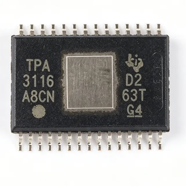
TPA3116D2DADR - 50W Stereo Class-D Audio Amp | Texas Instruments
The Texas Instruments TPA3116D2DADR is a filter-free, analog-input Class-D stereo audio amplifier delivering 2 x 50 W into 4-ohm speakers (or 100 W mono BTL into 2 ohms) from a 4.5 V to 26 V supply, packaged in a 32-pin HTSSOP (DAD) with exposed thermal pad. A Class-D audio amplifier is a switching amplifier whose output transistors operate as switches rather than linear elements, achieving efficiency above 85-90 percent. In the amplifier IC hierarchy, it sits under audio amplifiers, within the broader linear-amplifier IC family, and replaces bulky Class-AB stages plus heat sinks in compact speaker systems. Key features include filter-free operation with an integrated feedback loop that tolerates speaker inductance without an LC output filter, SpeakerGuard amplitude limiting that protects speakers from over-power events, and an AM-avoidance modulation scheme that keeps switching harmonics out of the AM broadcast band. Differential analog inputs improve common-mode noise rejection, and integrated short-circuit and thermal shutdown protection raise system robustness. The device uses an AD modulation topology with 250 kHz-class switching, so high efficiency eliminates heat sinks in most 2 x 50 W designs on a two-layer PCB with adequate copper pour. Fixed internal gain options and a master/slave-capable architecture simplify multi-channel designs; power-supply pumping is managed by the BTL configuration at low frequencies. Typical applications include Bluetooth and active speakers, soundbars, TV audio, portable PA and karaoke systems, and automotive/infotainment speaker drivers where efficiency and small size matter. Design consideration: at 2 x 50 W, PCB copper area under the exposed pad is the primary thermal path - provide a solid ground pour with thermal vias, and place supply decoupling (at least 10 uF bulk plus 0.1 uF ceramic) close to PVCC pins to minimize supply ripple and EMI. This page synthesizes distributor pricing, drop-in alternatives, comparison tables, and practical design notes not found in the manufacturer datasheet. Pricing below as of 2026-08-29.

TSHA4401 - 875nm GaAlAs IR Emitter, 3mm T-1 | Vishay
The Vishay TSHA4401 is a high-efficiency GaAlAs (Gallium Aluminum Arsenide) infrared emitting diode molded in a clear, untinted 3 mm (T-1) through-hole package with a 40-degree viewing angle. Built on GaAlAs-on-GaAlAs heterojunction technology, it emits at a peak wavelength of 875 nm and delivers typical radiant intensity of 16 mW/sr at 100 mA forward current, with a maximum forward current rating of 100 mA and a typical forward voltage of 1.5 V. The device supports high-speed switching with typical rise and fall times of 600 ns each, making it suitable for pulsed IR communication, optical encoders, and reflective sensors. An infrared emitting diode (IRED) is a semiconductor light source that emits near-infrared radiation (typically 700 nm to 1100 nm) when forward-biased. Unlike visible-light LEDs that target human-perceivable wavelengths, IREDs are paired with photodetectors or phototransistors to create optoelectronic links. In the component hierarchy, the TSHA4401 sits within optoelectronics -> LEDs -> infrared emitters -> GaAlAs IREDs. The 875 nm wavelength is particularly favored because it exhibits low absorption in standard glass, enabling operation through transmissive panes in industrial enclosures, automotive windows, and household appliances. Key differentiating features include high radiant intensity (16 mW/sr typical at 100 mA), narrow 40-degree beam angle for focused emission, fast switching with 600 ns rise/fall times, and a wide operating temperature range of -40C to +85C. Compared to standard GaAs-on-GaAs emitters at similar drive currents, the GaAlAs construction typically delivers several times the radiant intensity, allowing longer link distances or lower drive current for equivalent optical output. The 875 nm wavelength is matched to common silicon photodetectors (BPW34, BPV10) whose peak spectral response lies in the 850-950 nm band, maximizing receiver sensitivity without requiring special infrared filters. Architecturally, the TSHA4401 uses a double-heterojunction GaAlAs active region sandwiched between wider-bandgap AlGaAs cladding layers, which confines carriers to the active zone and boosts internal quantum efficiency. The molded epoxy lens is spectrally matched to the 875 nm emission and forms a narrow optical aperture that defines the 40-degree half-angle. The device is electrically a standard two-terminal diode - anode and cathode through radial leads - with no integrated driver, ESD clamp, or current-limiting resistor; the application circuit must provide a current source or series resistor. Typical applications include IR data transmission (IrDA-like links), optical encoders and interrupter modules, reflective object sensors, industrial remote controls, smoke and particulate detectors, and automotive interior sensing through glass panels. The 875 nm wavelength also aligns with night-vision camera sensitivity bands used in surveillance and machine vision. When designing with the TSHA4401, drive the LED with a controlled current source (or a resistor calculated from (Vsupply - Vf)/If) and add a small NPN transistor or MOSFET for high-frequency modulation - direct logic-level drive without current limiting will damage the junction. Decoupling the supply near the driver reduces conducted noise on nearby analog stages. For long-range links, pulse the LED at 100 mA peak rather than continuous DC to maximize radiant intensity while staying within the average power dissipation budget of 180 mW.
TSHA4401-AS12Z - 875nm GaAlAs IR Emitter, 3mm T-1 | Vishay
The Vishay TSHA4401-AS12Z is a high-efficiency gallium-aluminum-arsenide (GaAlAs) infrared emitting diode housed in a 3 mm (T-1) tinted diffused plastic package, with through-hole radial leads. It emits at a peak wavelength of 875 nm, delivers a typical radiant intensity of 16 mW/sr at 100 mA DC forward current, and supports a continuous forward current up to 100 mA with a forward voltage of approximately 1.5 V. The -AS12Z suffix designates the tape-and-reel lead-forming option, and the half-power emission angle is specified at ±20° (±40° total). An infrared emitter (IRED) is a semiconductor optoelectronic device that converts electrical current into near-infrared light, typically used in pairs with photodetectors or phototransistors to form an optical link. Within the optoelectronics hierarchy, an IRED falls under LEDs and Optoelectronics, with hypernyms IR LED, infrared emitter, GaAlAs IRED, and narrow-spectrum photo source. IR emitters are foundational building blocks for non-contact object detection, position sensing, data communication over light, and barrier/through-beam switches. The 875 nm wavelength is particularly chosen for its low attenuation through standard soda-lime glass, enabling applications where the emitter and detector are placed behind glass panes. Key features of the TSHA4401-AS12Z include a typical radiant power efficiency that is markedly higher than conventional GaAs IR emitters of its generation, a hermetically robust molded plastic package with viewing angle of ±20°, and fast switching speed suitable for pulsed modulation at tens of kHz. The 1.5 V typical Vf at 100 mA allows the device to be driven directly from low-voltage rails (3.3 V or 5 V) through a simple series resistor. Operating temperature spans -40 °C to +85 °C, covering industrial and consumer environments. Typical applications for this part include IR data transmission (IrDA-style links and remote-control carrier modulation), reflective and through-beam object sensors, industrial counters and tachometers, photo-interrupter modules, and glass-pane-barrier intrusion detectors. The narrow ±20° beam suits point-to-point links where off-axis rejection of ambient light is critical. When designing with this emitter, drive the LED with a constant-current source or a properly sized series resistor. Estimate the resistor value as R = (VCC - Vf) / If; for VCC = 5 V, Vf = 1.5 V, and If = 100 mA, R ≈ 35 Ω. A 100 nF bypass capacitor across the supply improves noise immunity. For pulsed operation, respect the peak forward current and duty cycle limits stated in the manufacturer datasheet.
VOS617A-4T - 3750Vrms Phototransistor Optocoupler, SSOP-4 | Vishay
The Vishay VOS617A-4T is a phototransistor-output optocoupler housed in a 4-pin SSOP (50 mil lead pitch, mini-flat) package, providing 3750 Vrms of galvanic isolation between input and output. The device uses a GaAs infrared emitting diode optically coupled to a silicon planar phototransistor detector, with a current transfer ratio (CTR) graded from 160% to 320% at a 5 mA forward current. The -4 CTR bin is positioned in the middle of the VOS617A family range, giving designers a balanced combination of high gain and predictable switching performance. A phototransistor optocoupler is a type of optoisolator that transfers electrical signals between two circuits using a light beam inside an electrically insulating package. The internal LED emits infrared light when forward-biased, and the phototransistor on the receiving side conducts proportionally to the received light intensity. This category belongs to the broader optocoupler / opto-isolator family, which itself sits within isolator ICs and discrete optoelectronic components used for safety isolation, ground-loop elimination, and high-voltage signal interfacing in industrial, medical, and switching power supply designs. Key features include a low forward voltage of approximately 1.1 V at 10 mA, a collector-emitter voltage of 80 V, and a low coupling capacitance that preserves signal integrity in high-speed digital interfaces. The device supports an operating temperature range of -55 °C to +110 °C, enabling deployment in harsh industrial environments. With a low typical input current requirement and SSOP-4 footprint of approximately 4.4 mm x 3.85 mm, the VOS617A-4T enables compact PCB layouts where board real estate is at a premium. The architecture combines a GaAs IR emitter with a silicon planar phototransistor detector in a half-pitch mini-flat package. Compared with DIP-4 optocouplers, the SSOP-4 form factor reduces board footprint by roughly 70%, while maintaining 3750 Vrms isolation - well above the requirements of most IEC 62368-1 reinforced insulation applications. The planar phototransistor process also gives lower dark current than conventional mesa phototransistors, improving noise immunity in low-signal designs. Typical applications include digital logic interfacing between low-voltage microcontrollers and high-voltage industrial buses, isolated gate drive feedback in switch-mode power supplies, PLC input/output isolation modules, and AC line detection circuits. The wide CTR range and high isolation voltage also make it suitable for medical equipment requiring patient-applied circuit protection. When designing with this device, place a bypass capacitor in parallel with the input LED to filter high-frequency noise, and verify that the CTR derating curve over temperature is acceptable for the minimum expected gain at the lowest operating temperature of your application. Also confirm that the load resistor value does not exceed the maximum collector current rating under worst-case CTR. This page synthesizes Vishay datasheet parameters, distributor stock and pricing data, drop-in compatible alternatives, and practical design notes that extend beyond the manufacturer's datasheet presentation.
XL-HD3535SURC-A2 - 1W 3535 Red LED, 350mA, 625nm | XINGLIGHT
The XINGLIGHT XL-HD3535SURC-A2 is a high-power red LED in a 3.5 x 3.5 x 2.2 mm SMD-3535 package with a transparent water-clear colloid, optimized for camera flash, flashlight, and high-intensity general lighting applications. It delivers 40-60 lm of luminous flux at a dominant wavelength of 615-625 nm (typ. 625 nm), driven at a forward current of 350 mA with a forward voltage of 1.8-2.4 V. The viewing angle is 130 degrees, providing broad and even light distribution in compact optical assemblies. A high-power LED is a semiconductor light source that converts electrical energy into light with higher current density and luminous flux than standard indicator LEDs, requiring constant-current drive and thermal management to maintain reliability. Within the LED taxonomy, the XL-HD3535SURC-A2 falls under high-power LEDs, which sit between standard indicator LEDs (typically 20 mA) and LED COB/CSP modules (>5 W). Its 3535 metric footprint places it in the mid-power surface-mount category used in portable, automotive, and architectural lighting fixtures. Key features include a 1 W power rating, a peak pulsed forward current capability above 350 mA, an electrostatic discharge threshold consistent with JEDEC MSL-3 handling, and a wide operating temperature range of -40C to +85C. The epoxy resin lens is water-clear, allowing maximum luminous intensity with minimal color absorption. The 130-degree beam profile enables wide-area illumination without secondary optics. Technically, the device uses an AlGaInP (aluminum gallium indium phosphide) epitaxial structure on a GaAs substrate, the standard material system for high-brightness red and amber LEDs in the 615-630 nm band. The 3535 ceramic-look package supports efficient heat transfer from the die junction to the PCB land pad, which doubles as the thermal pad. Junction-to-ambient thermal resistance is on the order of 20-30 C/W per JEDEC standard test conditions. Typical applications include camera phone flashes, tactical flashlights, decorative stage lighting, signage and beacon systems, automotive interior/exterior accent lighting, and high-end indicator strips. The 625 nm dominant wavelength produces a saturated deep-red color well-suited for warning indicators and decorative effects. When designing with the XL-HD3535SURC-A2, drive it with a constant-current source rather than constant voltage to avoid thermal runaway. Provide adequate copper area (typically >= 25 mm^2) under the thermal pad to keep the junction below 125C at full 350 mA drive. This page synthesizes distributor pricing, drop-in alternatives, and practical design notes not found on a single manufacturer product page, giving engineers and procurement teams an information gain over standard distributor listings.