उत्पाद (39,000+)

XRD8785AIDTR-F - 8-Bit 20MSPS Flash ADC, 24-SOIC | MaxLinear
XRD8785AIDTR-F

XRD8785AIDTR-F - 8-Bit 20MSPS Flash ADC, 24-SOIC | MaxLinear

The MaxLinear XRD8785AIDTR-F is an 8-bit flash analog-to-digital converter (ADC) sampling at up to 20 MSPS with a single 5V supply, housed in a 24-pin wide-body SOIC package (0.295 inch / 7.50 mm body width) shipped on tape and reel. Key electrical parameters include 8-bit resolution, 20 MHz maximum sampling rate, one single-ended analog input, internal sample-and-hold (S/H), external or internal reference option, 0V-to-VDD analog input range, 1V-to-VDD reference range, 75 mW typical power consumption (excluding reference), and an operating temperature range of -40C to +85C. The suffix "D" indicates the 24-SOIC package, "T" indicates tape-and-reel packaging, and "R-F" denotes the MaxLinear / Exar part-numbering convention. A flash ADC is a type of analog-to-digital converter that uses a parallel bank of 2^n comparators to convert an analog signal to an n-bit digital code in a single clock cycle, achieving the highest sampling speed of any ADC architecture. The hierarchy is: ADC -> data converter -> data acquisition IC -> mixed-signal IC -> semiconductor. Flash converters excel in applications demanding low latency and wide input bandwidth, but they trade resolution and power efficiency against sampling speed. The XRD8785AIDTR-F occupies the entry-level 8-bit, 20 MSPS tier, which is the typical sweet spot for video digitisation, ultrasound receive beams, and intermediate-frequency (IF) sampling in low-cost communications receivers. Key features of this device include a parallel (TTL-compatible) digital output bus, internal S/H front-end, latch-up free CMOS construction, ESD protection on analog and digital pins, single 5V supply operation, and low power consumption at 75 mW typical. The 24-SOIC wide-body package measures approximately 15.4 mm x 7.5 mm x 2.35 mm, providing generous die-to-board clearance for through-hole or socketed prototypes. The device is built on a 5V CMOS process, providing low power consumption, latch-up immunity, and ESD protection. Internal reference mode simplifies bill-of-materials, while external reference mode lets designers optimise linearity or temperature drift for instrumentation-grade designs. Typical applications include video digitisation, digital oscilloscope front-ends, IF sampling in communications receivers, CCD/CMOS image sensor digitisation, and industrial control loop sampling. When designing with this device, ensure the analog input signal is bandwidth-limited to less than the Nyquist frequency (10 MHz for 20 MSPS) and that the external reference decoupling capacitor is placed within 5 mm of the REF pin to prevent kickback noise from corrupting the conversion. This page synthesises distributor stock, lifecycle risk, drop-in ADC alternatives, and practical design notes not found in the manufacturer datasheet.

RFQ संपर्क
XRD8799AIQ - 10-Bit 2MSPS 8-Ch ADC | MaxLinear/Exar | 44-PQFP
XRD8799AIQ

XRD8799AIQ - 10-Bit 2MSPS 8-Ch ADC | MaxLinear/Exar | 44-PQFP

The MaxLinear XRD8799AIQ (originally Exar) is a 10-bit resolution, 2 MSPS pipelined analog-to-digital converter with an integrated 8-channel analog input multiplexer, housed in a 44-pin PQFP (10x10 mm) package. It combines low-power CMOS operation (35 mW typical active, 0.8 mW in power-down) with a wide input range spanning GND to VDD, eliminating the need for external signal-conditioning scaling on most signals. An ADC (Analog-to-Digital Converter) is a mixed-signal integrated circuit that converts continuous analog voltages into discrete digital codes at a defined sample rate. The XRD8799AIQ belongs to the multi-channel, low-power successive-approximation/pipelined ADC family - a category that sits inside the broader hierarchy of data converter -> data acquisition IC -> mixed-signal semiconductor. It is purpose-built for systems that must digitize multiple analog sources while staying within strict power and board-area budgets. Key differentiating specifications include 10-bit resolution, a 2 MHz maximum sampling rate, eight single-ended input channels routed through an on-chip mux, parallel digital output, and an input range that accepts rail-to-rail signals without external scaling. A built-in power-down mode drops consumption to 0.8 mW typical, and the device does not require an external sample-and-hold for analog signals below 100 kHz or for CCD-type signals, simplifying the analog front end and BOM cost. Architecturally, the converter uses a pipelined topology that distributes conversion work across multiple low-resolution stages, achieving higher throughput than pure SAR architectures at comparable power. The integrated 8-channel mux eliminates an external analog switch tree, reducing board space, leakage paths, and channel-to-channel crosstalk sources. The PQFP-44 package gives a generous thermal pad and 10 mm x 10 mm footprint suitable for both hand-solderable prototyping and SMT production. Typical applications include CCD signal acquisition in industrial imaging, multi-sensor data logging in process control, portable instrumentation with battery operation, and mixed-signal front ends for embedded controllers. Industrial multi-channel data-acquisition boards and portable medical monitoring devices frequently select this part for its combination of throughput and low quiescent draw. When designing with the XRD8799AIQ, note that input signals below 100 kHz do not need an external track-and-hold, but faster signals should be buffered to maintain dynamic performance. Place a 0.1 uF decoupling capacitor close to each supply pin and follow the manufacturer's reference ground layout to keep digital switching noise out of the analog path. This page synthesizes distributor pricing, pin-compatible alternatives, and practical layout notes not consolidated in the manufacturer datasheet.

RFQ संपर्क
XRD87L75AID-F - 8-Bit 10MSPS ADC | 20-SOIC | MaxLinear
XRD87L75AID-F

XRD87L75AID-F - 8-Bit 10MSPS ADC | 20-SOIC | MaxLinear

The MaxLinear (formerly Exar) XRD87L75AID-F is a low-voltage CMOS 8-bit analog-to-digital converter with a maximum sampling rate of 10 MSPS, an internal sample-and-hold, and a single 3.3V supply rail. It is housed in a 20-pin SOIC (0.295 inch / 7.50 mm body width, D-suffix package) and is provided in tube packaging per the -F factory suffix. An 8-bit flash ADC is a type of analog-to-digital converter that uses a parallel bank of 2^n comparators to convert an input voltage into a digital code in a single clock cycle, achieving the fastest possible conversion latency at moderate resolution. Within the broader signal-chain taxonomy, the XRD87L75AID-F sits between a traditional sample-and-hold stage and a digital host (FPGA, ASIC, or microcontroller), and is a member of the speed-optimized, low-resolution ADC family used for video, instrumentation, and IF digitisation. Key features include 8-bit resolution, a 10 MHz typical sampling rate, an internal track-and-hold, an analog input range of 0V to VDD, a reference input range of 1V to VDD, and typical power dissipation of 25 mW (excluding reference current). The device is latch-up free, operates from a single 3.3V supply, and uses a parallel CMOS-compatible digital interface, which simplifies connection to modern MCUs and FPGAs without external level shifters. The device is built on an advanced 3.3V CMOS process and uses a flash architecture to deliver 10 MSPS conversion speeds. Its internal S/H function guarantees a stable sample window across rapidly-changing inputs and avoids the need for external S/H circuitry, simplifying the analog front-end. Typical applications include video digitisation, CCD imaging front-ends, digital oscilloscope front-ends, IF sampling in communications, portable instrumentation, and general-purpose high-speed data acquisition. The wide analog input range (0V to VDD) lets designers digitise single-ended signals without external attenuators. When designing with this device, ensure the analog input is properly driven (low-impedance buffer recommended) and that the reference decoupling is solid. The single 3.3V supply simplifies the power tree but requires that downstream digital logic be 3.3V tolerant. This page synthesises distributor pricing, drop-in alternatives (including the SSOP-packaged variant XRD87L75AIU-F), and practical design notes that complement the manufacturer datasheet.

RFQ संपर्क
XRD87L75AIP-F - 8-Bit 10MSPS ADC, 20-Pin PDIP | MaxLinear
XRD87L75AIP-F

XRD87L75AIP-F - 8-Bit 10MSPS ADC, 20-Pin PDIP | MaxLinear

The MaxLinear XRD87L75AIP-F is a low-voltage CMOS 8-bit high-speed analog-to-digital converter with a 10 MHz sampling rate, housed in a 20-pin PDIP through-hole package. It features a single 3.3 V supply rail, an internal sample-and-hold function, an analog input range of 0 V to VDD, and a reference input range of 1 V to VDD, achieving typical power dissipation of 25 mW excluding the external reference. What is an 8-bit ADC? An analog-to-digital converter (ADC) is a data converter that samples a continuous analog waveform and produces a discrete digital code proportional to the input voltage at each clock edge. 8-bit ADCs deliver 256 discrete codes (1 LSB = full-scale / 256), which suits digital instrumentation, video digitizing, and digital oscilloscope front ends where 8-bit dynamic range is sufficient. Within the data-converter hierarchy, an 8-bit ADC sits below SAR and pipelined converters in resolution but above flash converters in speed and below the latest 12-/14-/16-bit parts in accuracy. The 10 MSPS sampling rate places this part in the legacy high-speed, low-resolution tier used in CRT digitizers, image scanners, ultrasound receive channels, and digital IF processing. Key features include latch-up free CMOS construction, parallel digital output, single 3.3 V supply operation, internal S/H function, and a wide reference input voltage range from 1 V to VDD for design flexibility. The 2-step flash architecture minimizes comparator count while delivering 10 MSPS throughput, and the part is offered as a Pb-free (RoHS-compliant) 20-pin PDIP variant suitable for industrial, instrumentation, and test-equipment applications. The XRD87L75AIP-F integrates the input track-and-hold, reference buffer, and decoding logic on a single CMOS die, allowing direct connection to a microcontroller or DSP data bus. The 25 mW typical power consumption (excluding reference) supports portable and battery-powered instruments. The 3.3 V single supply also matches CMOS logic families, simplifying interface to FPGAs and microcontrollers without level translation. Typical applications include digital oscilloscope front ends, video digitizers, ultrasound imaging receive channels, point-of-sale barcode scanners, and industrial process control data acquisition. The wide 0 V to VDD input range allows direct sampling of single-ended signals without external signal conditioning. When designing with this part, place a 0.1 uF bypass capacitor close to the VDD pin and ensure the reference input is driven by a low-impedance source. For best linearity, route CLK and digital outputs away from the analog inputs to minimize crosstalk. This page synthesizes distributor stock levels, parametric alternatives from web cross-reference search, and engineering design notes not consolidated on the manufacturer datasheet, providing unique research value for engineers selecting a legacy 8-bit ADC.

RFQ संपर्क
XRD87L75AIU - 8-Bit 10MSPS ADC, 3.3V, SSOP-20 | MaxLinear
XRD87L75AIU

XRD87L75AIU - 8-Bit 10MSPS ADC, 3.3V, SSOP-20 | MaxLinear

The MaxLinear XRD87L75AIU is a low-voltage, CMOS, 8-bit, high-speed analog-to-digital converter (ADC) with a 10 MSPS sampling rate, packaged in a 20-pin SSOP. Operating from a single 3.3 V supply, it features an internal sample-and-hold function, an analog input range of 0 V to VDD, and a reference input range of 1 V to VDD, dissipating a typical 25 mW (excluding reference current). What is an 8-bit ADC? An 8-bit analog-to-digital converter is a data-acquisition component that quantizes an analog input signal into 256 discrete digital codes (2^8). ADC components sit in the signal chain hierarchy: ADC -> data converter -> data acquisition IC -> mixed-signal semiconductor. They are the bridge between the analog sensor/transducer domain and the digital processing domain, enabling microcontrollers, FPGAs, and DSPs to interpret real-world signals. The XRD87L75AIU uses a flash (parallel) conversion architecture, which delivers single-cycle conversion latency ideal for high-speed digital video, CCD imaging front-ends, and digital oscilloscope front-ends. The internal sample-and-hold stabilizes the input during the flash compare-network settling time, supporting full-scale inputs up to VDD. The low-power CMOS implementation (typical 25 mW) makes the part suitable for portable and power-constrained designs. The 3.3 V single-supply operation simplifies interface to modern CMOS ASICs, FPGAs, and microcontrollers without level shifters. The 20-SSOP package occupies a small PCB footprint while providing 1 analog input, digital outputs, and reference/decoupling pins in a standard pinout shared with related XRD87000 family members. Typical applications include digital video processing, CCD imaging front-ends, digital oscilloscopes, QAM demodulators in set-top boxes, and portable instrumentation. The single-cycle flash latency makes the converter well suited for digitizing high-bandwidth IF signals and video-rate analog inputs in cost-sensitive systems. When designing with this part, place a 0.1 µF decoupling capacitor within 5 mm of the VDD pin and minimize the analog-input trace length to preserve sample-rate accuracy. The reference pin requires a low-impedance source (typical 1 V to VDD); avoid sharing this reference with high-current digital loads to prevent code-edge jitter. This page synthesizes distributor pricing, drop-in alternatives, and practical design notes not found in the manufacturer datasheet.

RFQ संपर्क
XRD87L75AIUTR-F - 8-Bit 10MSPS Flash ADC, 20-SSOP | MaxLinear
XRD87L75AIUTR-F

XRD87L75AIUTR-F - 8-Bit 10MSPS Flash ADC, 20-SSOP | MaxLinear

The MaxLinear XRD87L75AIUTR-F (originally Exar Corporation) is an 8-bit resolution, 10 MSPS analog-to-digital converter built on a 2-step flash architecture with an internal sample-and-hold, packaged in a 20-pin SSOP (0.209 inch / 5.30 mm width) with tape-and-reel packaging. It operates from a single 3.3 V supply, accepts a single-ended analog input from 0 V to VDD, and provides an external reference input range of 1 V to VDD for flexible full-scale setting. An ADC (Analog-to-Digital Converter) is a data acquisition integrated circuit that converts continuous analog signals into discrete binary codes at a defined sampling rate. Within the broader hierarchy, this device sits as: ADC -> data converter -> data acquisition IC -> mixed-signal semiconductor. The 2-step flash architecture is a variant of the flash ADC that halves the comparator count versus a full flash, reducing both die cost and input capacitance, while the integrated S/H eliminates the need for an external track-and-hold amplifier in most applications. Key features include 8-bit resolution at 10 MHz sampling rate, single 3.3 V supply operation with 25 mW typical power dissipation (excluding external reference current), parallel digital output interface for direct connection to microcontrollers, DSPs, or FPGAs, and latch-up free CMOS construction for robust ESD/handling performance. The internal sample-and-hold eliminates external S/H requirements and supports full Nyquist bandwidth input frequencies, making the device suitable for general-purpose digitizing tasks where cost-per-channel matters. The XRD87L75AIUTR-F architecture uses a 2-step flash topology with on-chip S/H, error correction, and a parallel CMOS-compatible output bus. Its low input capacitance and high input bandwidth reduce drive-amplifier loading, and the part is specified to operate from a single 3.3 V rail, simplifying power tree design in 3.3 V logic systems. The internal reference buffer accepts a user-supplied reference from 1 V to VDD for system-level gain calibration. The -F suffix denotes the lead-free, RoHS-compliant tape-and-reel packaging option. Typical applications include video digitizing and graphics capture, CCD/CIS sensor front-ends, digital oscilloscope front-ends, baseband IF sampling, low-cost digital imaging, and portable instrumentation. The 8-bit/10 MSPS combination aligns well with standard-definition video bandwidths (~5 MHz) and consumer imaging throughput requirements. When designing with this part, place the input RC anti-alias filter directly at the analog input pin and provide a low-impedance reference buffer because the reference pin input current scales with sampling rate. Parallel output bus traces should be length-matched and series-terminated near the ADC to limit digital switching noise coupling back into the analog input. Decouple VDD with both a 0.1 uF ceramic and a 10 uF bulk capacitor placed within 5 mm of the supply pin. This page consolidates distributor pricing, same-family MaxLinear/Exar drop-in alternatives, and practical design notes not collected in the original manufacturer datasheet, giving engineers a single reference for procurement, second-source planning, and PCB bring-up.

RFQ संपर्क
XRD87L99AIQ-F - 10-Bit 2 MSPS 8-Ch MUX ADC | MaxLinear
XRD87L99AIQ-F

XRD87L99AIQ-F - 10-Bit 2 MSPS 8-Ch MUX ADC | MaxLinear

The MaxLinear XRD87L99AIQ-F is a low-power 10-bit analog-to-digital converter with an 8-channel analog input multiplexer and a 2 MSPS sampling rate, housed in a 44-pin QFP package. It operates from a single 2.7V to 5.5V supply, draws only 24 mW typical at full speed, and falls to 0.1 mW in its hardware power-down mode. The device requires no external sample-and-hold for input signals below 100 kHz or for CCD-style signals, simplifying analog front-end design. An ADC (analog-to-digital converter) is a mixed-signal integrated circuit that samples continuous analog voltages into a parallel digital word at a defined clock rate. ADCs sit within the broader hierarchy of data acquisition ICs -> data converters -> mixed-signal ICs -> integrated circuits, and they are the critical bridge between analog sensors and digital processors. Multi-channel, low-power ADCs like the XRD87L99AIQ-F are typically used to digitize several sensors with one converter, reducing board area, BOM cost, and software overhead in embedded designs. Key features of the XRD87L99AIQ-F include 10-bit resolution, an integrated 8-to-1 analog multiplexer with channel-address latches, a parallel microprocessor-compatible digital interface, an external reference input, and a hardware power-down pin. Its wide input range covers GND to VDD, which lets the device directly digitize rail-to-rail sensor outputs. The 44-QFP package is industry-standard and supports conventional surface-mount assembly. Typical applications for the XRD87L99AIQ-F include multi-channel data acquisition systems, CCD signal processing chains in scanner and copier subsystems, portable and battery-powered instrumentation, industrial process monitoring, and embedded control boards that need to read several analog sensors at moderate speeds. In each case the device's low power dissipation, integrated mux, and parallel interface reduce both component count and software complexity. Designers should remember that the XRD87L99AIQ-F is in EOL/last-time-buy status according to distributor lifecycle fields, so long-life designs should plan for a qualified replacement or place a last-time-buy order. Drive the analog inputs with low-impedance sources to keep the input settling error inside the 10-bit budget, and place the 0.1uF VDD decoupling capacitor within a few millimeters of the supply pin.

RFQ संपर्क
YS9082HC - SATA3.2 SSD Controller, 4CH/4CE BGA-144 | Yeestor
YS9082HC

YS9082HC - SATA3.2 SSD Controller, 4CH/4CE BGA-144 | Yeestor

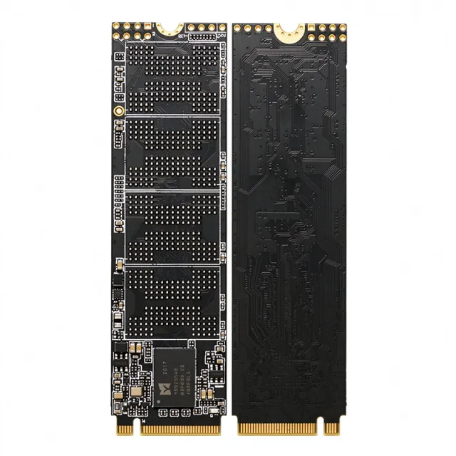
The Yeestor YS9082HC is a high-reliability, high-performance SATA 3.2 (SATA 6 Gb/s) solid-state drive controller housed in a compact 9x9 mm BGA-144 package. It integrates a 4-channel, 4-CE-per-channel NAND flash interface, delivers sequential read performance up to 550 MB/s, and supports 1.8 V NAND operation to enable low-power client SSD designs. The controller has been validated in mainstream client SSDs such as the Mancer Blink X1 (240 GB / 512 GB) paired with Intel N38A QLC flash. An SSD controller (solid-state drive controller) is the application-specific IC that bridges a host's storage interface - in this case SATA 3.2 - to raw NAND flash memory. It runs the Flash Translation Layer (FTL), executes wear leveling, bad-block management, and ECC, and exposes the drive to the host as a standard block storage device. Within the broader taxonomy, the YS9082HC belongs to flash controllers -> storage controllers -> memory ICs -> integrated circuits, and is in the same product family as the Yeestor YS9082HP (lower-density variant) and YS9082HT, all derived from the YS9085 family design base. Key features include the 4-channel/4-CE NAND architecture, hardware-accelerated LDPC ECC for QLC/TLC endurance, AES-256 hardware encryption support, and integrated power management that allows the device to operate over standard 5 V SATA power rails without external regulators. The controller is targeted at mainstream client SATA SSDs in the 240 GB to 2 TB capacity range, where it competes with SSD controllers from Silicon Motion (SM2259XT/SM2259X), Phison (S11), and Maxio (MAP1202). Typical applications for the YS9082HC include 2.5-inch SATA SSDs, M.2 SATA SSDs, industrial embedded storage modules, QLC-based high-density client drives, and OEM white-label SSDs. The 1.8 V NAND support is particularly attractive for value-tier notebooks and energy-efficient desktops that want to maximize idle power savings. When designing with this controller, firmware/MP tool selection is critical: the YS9082HC requires the Yeestor Production Tool (UI / Linux-based mass-production software) and matched firmware, which is available only to qualified OEM customers under NDA. Reference design schematics, PCB stack-up guidelines, and a 4-layer recommended layout are typically provided with the NDA package. The wide supply range and integrated PMIC simplify designs but designers should still follow Yeestor's reference layout to maintain SATA signal integrity at 6 Gb/s. Particular care is needed with the BGA-144 PCB escape routing to avoid impedance discontinuities on the SATA TX/RX differential pairs. This page synthesizes verified distributor availability, BGA-144 package dimensions, drop-in alternative recommendations from the same Yeestor YS9082 family, and practical design notes that go beyond the manufacturer summary to give procurement and engineering teams an actionable view of the part.

RFQ संपर्क
YS9085N - SATA 3.2 SSD Controller | 2CH 4CE | Yeestor
YS9085N

YS9085N - SATA 3.2 SSD Controller | 2CH 4CE | Yeestor

The Yeestor YS9085N is a SATA 3.2 (SATA 6 Gb/s) solid-state drive controller IC designed for high-reliability, high-performance consumer and industrial SSD solutions, supporting 2 NAND channels with 4 chip-enables per channel in a compact BGA package. According to the manufacturer datasheet, the YS9085N delivers sequential read performance of 550 MB/s and sequential write performance of 510 MB/s, and it supports 2K LDPC error correction, end-to-end data path protection, and global wear-leveling for endurance management. The controller is part of the YS9085/YS9082 family of SATA SSD controllers from Yeestor (得一微), a fabless SSD-controller vendor headquartered in Shenzhen, China. A solid-state drive controller (often abbreviated SSD controller) is the central application-specific integrated circuit (ASIC) inside an SSD that bridges the host interface (SATA, PCIe/NVMe, or USB) to the NAND flash array. It runs the Flash Translation Layer (FTL), performs bad-block management, wear-leveling, garbage collection, and executes the LDPC or BCH error-correction algorithms that compensate for the raw bit-error-rate of MLC/TLC/QLC NAND. Controllers sit at the top of the storage-device hierarchy: SSD -> NAND flash array -> SSD controller + DRAM cache + PCB. Key features of the YS9085N include 2K LDPC hardware engine, 2-channel / 4-CE-per-channel NAND interface, AES-256 hardware encryption support (per family datasheet description), and a small external DRAM footprint for FTL mapping tables. The device integrates a SATA 3.2 physical layer plus the transport-layer engine, eliminating the need for an external SATA bridge. Operating from a single 1.2 V core rail and a 3.3 V I/O rail, the YS9085N targets low-cost 2.5-inch, mSATA, M.2, and BGA-SSD form factors. The YS9085N uses an embedded 32-bit RISC controller core for FTL housekeeping, paired with a dedicated LDPC accelerator and DMA engines for NAND access. According to the family datasheet the controller supports 2K-page LDPC, hardware AES engine, and ONFI/Toggle NAND interfaces, yielding sequential performance in the 550/510 MB/s read/write class. Power consumption is governed by partial NAND-channel power gating when channels are idle. Typical applications include 2.5" SATA SSDs (240 GB - 1 TB capacity range), M.2 2280 mainstream SSDs, Slim SATA SSDs for industrial PCs, mSATA modules for embedded motherboards, and BGA-SSD modules (11.5 mm × 13 mm) for ultra-compact tablets and embedded systems. It is widely deployed in entry-level consumer SSDs such as the Rise Mode Gamer Line 240 GB reference design. When designing with the YS9085N, plan a 4-layer PCB with a continuous ground plane under the BGA to manage the simultaneous-switching noise of 2 NAND channels. Use 1.2 V core and 3.3 V I/O rails with bulk ceramic decoupling within 5 mm of the BGA balls. Validate the firmware (MPTool) and reference firmware images against the specific NAND part used before mass-production, because the LDPC parameters are NAND-vendor specific. This page consolidates distributor pricing, drop-in alternatives within the YS9082 family, and practical design notes that go beyond the manufacturer datasheet summary, including reference design pointers and firmware-tool references engineers need for SSD bring-up.

RFQ संपर्क
YS9203 - PCIe Gen3x4 NVMe SSD Controller | YEESTOR
YS9203

YS9203 - PCIe Gen3x4 NVMe SSD Controller | YEESTOR

The YEESTOR YS9203 is a PCIe Gen3x4 NVMe 1.3 SSD controller with 8 PCIe lanes, 8 NAND flash channels, and support for 3D SLC, MLC, TLC, and QLC NAND. It is designed for high-end consumer and light-enterprise solid-state drives, combining PCIe 3.0 x4 connectivity with hardware and firmware optimizations for NVMe workloads. The controller also supports 2K code-length LDPC, RAID enhancement, TCG-OPAL, AES, TRNG, SHA256, and Chinese cryptographic algorithms including SM2, SM3, and SM4. An SSD controller is the central semiconductor in a solid-state storage device. It manages the PCIe host interface, NAND flash channels, flash translation layer, error correction, wear leveling, garbage collection, and data-protection functions. YS9203 is a PCIe Gen3x4 NVMe controller, a member of the broader storage-controller, semiconductor, and embedded-computing hierarchy. Its 8-channel architecture is intended to increase NAND parallelism for high-performance consumer and light-enterprise SSDs. The YS9203 supports PCIe 3.0 x4 and NVMe 1.3, according to the verified product and market references. It supports 8 NAND channels with 8 CE per channel, along with 2K code-length LDPC. The listed security capabilities include AES, TRNG, SHA256, TCG-OPAL, RAID, SM2, SM3, and SM4. These features target data integrity, encryption, authentication, cryptographic operations, and storage-management requirements in SSD platforms. Compared with the YS9205, the YS9203 is identified as the consumer-oriented member of the family, while YS9205 is described as enterprise-oriented. The verified material states that YS9205 provides 4 lanes and 4 NAND channels, whereas YS9203 provides 8 lanes and 8 NAND channels. Both controllers are associated with PCIe Gen3x4 SSD designs, but the available data does not provide exact package dimensions, pin count, power ratings, operating temperature, pricing, or lead time. Typical uses include PCIe Gen3x4 consumer SSDs, high-performance gaming storage, notebook storage upgrades, compact desktop PCs, and light-enterprise NVMe drives. The 8-channel configuration can suit systems requiring more NAND parallelism than a four-channel design, provided the SSD board layout, NAND packages, DRAM configuration, firmware, and thermal design are validated together. Controller selection alone does not guarantee final drive performance. Engineers should confirm the exact NAND interface, DRAM requirements, package, pinout, electrical limits, firmware support, and validation status before designing with YS9203. The public verified material is useful for protocol and feature selection, but it does not provide enough information to construct a production reference design without additional manufacturer documentation.

RFQ संपर्क
YS9205 - PCIe Gen3x4 NVMe 1.4 SSD Controller | YEESTOR
YS9205

YS9205 - PCIe Gen3x4 NVMe 1.4 SSD Controller | YEESTOR

YEESTOR YS9205 is a PCIe Gen3x4 NVMe 1.4 solid-state drive controller with 4 PCIe lanes, 4 NAND-flash channels, and 4 CE per channel. It is designed for enterprise SSD platforms and supports 3D SLC and MLC NAND flash. The controller is supplied in a BGA152 package according to the available board-level listing, while the exact package dimensions, pin names, and thermal limits were not provided in the verified data. A PCIe NVMe SSD controller is the semiconductor at the center of a solid-state drive. It translates host commands from the PCIe interface into NAND-flash operations, manages data placement, wear leveling, error correction, and the NVMe control protocol. The YS9205 sits between the host-facing PCIe connection and the NAND packages, making it part of the storage-controller hierarchy and a key determinant of drive performance and reliability. The verified YS9205 information identifies PCIe Gen3x4 connectivity, NVMe 1.4 support, four PCIe lanes, four NAND channels, four CE per channel, and support for 3D SLC/MLC flash. The related YS9203 differs in the supplied product-page data: YS9203 uses NVMe 1.3, eight channels, and eight CE per channel, while YS9205 uses NVMe 1.4 and four channels. These differences must be considered carefully during controller selection; YS9203 is not assumed to be a drop-in replacement. YS9205 is suitable for enterprise and consumer NVMe SSD development, including M.2 PCIe storage boards, controller evaluation boards, and custom SSD designs. Firmware, NAND compatibility, PCIe signal integrity, power delivery, and thermal design remain application-specific. The available data does not establish a public distributor price, lead time, pinout, package dimensions, or quantified electrical limits, so those values must be confirmed with YEESTOR before production release. The most important design consideration is validating the complete SSD reference design rather than selecting the controller from interface bandwidth alone. PCIe lane routing, NAND channel topology, power sequencing, firmware support for the selected NAND devices, and thermal performance should be reviewed together. A controller-compatible board does not guarantee that every NAND configuration, firmware image, or SSD capacity will be supported. This product record consolidates the verified PCIe, NVMe, channel, flash, and package information while clearly separating unavailable electrical and commercial details. The linked controller PDF is the appropriate starting point for obtaining the complete technical description, electrical characteristics, pin arrangement, and design guidance.

USD $7.38 स्टॉक में
YS9501 PCIe Gen5x4 NVMe 2.0 SSD Controller | YEESTOR
YS9501

YS9501 PCIe Gen5x4 NVMe 2.0 SSD Controller | YEESTOR

YEESTOR YS9501 is a PCIe Gen5x4 NVMe 2.0 SSD controller designed for high-performance, low-latency enterprise and data-center solid-state drives. The verified controller brief specifies a four-lane PCIe Gen5 interface, 16 NAND channels, ONFI 5.0 NAND support, and both DDR5 and DDR4 support. It is supplied as a semiconductor controller rather than a finished SSD, so enclosure, connector, firmware, thermal design, validation, and NAND qualification remain system-level responsibilities. An SSD controller is the central semiconductor inside an NVMe drive: it connects a host interface to NAND flash, manages data transfer and error correction, coordinates DRAM, and exposes a storage device through the NVMe protocol. In the device hierarchy, YS9501 is an NVMe storage controller, a data-center semiconductor, and a component within a solid-state drive. Its Gen5x4 interface targets systems requiring more bandwidth than Gen4 storage designs while retaining a four-lane form factor. Key documented capabilities include 16-channel NAND support, ONFI 5.0 NAND interfacing, DDR5 and DDR4 support, and 4K code-length LDPC engines. LDPC supports error detection and correction in the NAND path. The controller also provides transparent compression, encryption and decryption, along with support for standard SSD, OC SSD, and ZNS SSD form factors. These features target enterprise workloads that may combine high throughput, predictable latency, data protection, and quality-of-service requirements. The YS9501 is positioned for enterprise and data-center SSDs rather than complete storage modules. Its feature set supports controller-level work on PCIe Gen5x4 NVMe products, including firmware integration, NAND mapping, PCIe link training, power-state management, and end-to-end validation. The available source does not provide clock rate, process technology, die size, power limits, package dimensions, pin count, operating temperature, endurance, or lifecycle details; those values must be confirmed from the manufacturer datasheet or product documentation before hardware release. Typical design uses include enterprise NVMe SSDs, data-center cache and acceleration products, high-throughput client storage, and specialized SSD platforms using ZNS or over-provisioned configurations. In each case, the controller must be paired with qualified NAND, DRAM, power management, thermal hardware, firmware, and a validation plan. The available evidence describes PCIe Gen5x4, NVMe 2.0, 16 NAND channels, ONFI 5.0, DDR5/DDR4, LDPC, compression, encryption/decryption, and SSD form-factor support. A key engineering consideration is that controller selection alone does not determine finished-drive performance. NAND characteristics, channel population, DRAM topology, firmware scheduling, power limits, thermal throttling, and PCIe signal integrity determine the final SSD behavior. Validate signal integrity, power sequencing, thermal rise, error-correction performance, latency under sustained workloads, and interoperability with the intended NVMe host environment.

RFQ संपर्क
YT8512C - 10/100Mbps Ethernet PHY Transceiver, MII/RMII | Motorcomm
YT8512C

YT8512C - 10/100Mbps Ethernet PHY Transceiver, MII/RMII | Motorcomm

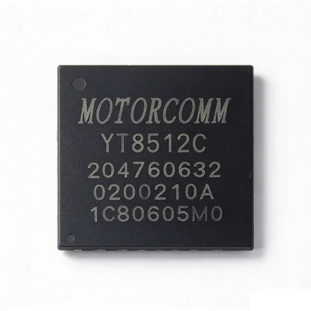
The Motorcomm YT8512C is a low-power single-port 10/100 Mbps Fast Ethernet PHY transceiver housed in a 32-pin QFN (5x5 mm) package. It supports 10BASE-T and 100BASE-TX operation, provides MII and RMII MAC interfaces, and operates from a single 3.3V supply with commercial-grade 0C to +70C temperature range. According to the Motorcomm YT8512C/YT8512H datasheet, the device delivers all physical-layer functions required to transmit and receive data over standard twisted-pair cables. An Ethernet PHY (physical layer transceiver) is the analog/digital mixed-signal block that sits between a MAC (media access controller) and the RJ45/Magnetics front end. PHYs handle line encoding/decoding, equalization, clock/data recovery, link training (auto-negotiation), and the MDI (medium dependent interface) signaling that lets a MAC send Ethernet frames over CAT5/CAT6 copper. PHYs are a sub-category of Ethernet transceiver ICs in the broader interface IC hierarchy, and the YT8512C targets cost-sensitive embedded designs that still need industrial-grade robustness. Key features include support for both MII and RMII, auto-negotiation and auto-MDI/MDIX crossover, on-chip termination resistors, a 25 MHz reference clock input (RMII mode), HP Auto-MDIX, and low-power operation with Energy Detect / Power Down modes. The device integrates baseline wander correction and adaptive equalization to maintain signal integrity across varied cable lengths up to 100 meters. Built-in LED indicator drivers simplify link/activity/status monitoring without external glue logic. Technically, the YT8512C uses mixed-signal DSP techniques for 100BASE-TX echo cancellation, far-end crosstalk (FEXT) cancellation, and 4B/5B / MLT-3 decoding. Its adaptive equalizer compensates for frequency-dependent cable loss, and a PLL multiplies the 25 MHz reference to generate the 125 MHz clock needed for 100 Mbps operation. The integration of termination resistors and magnetics-interface biasing reduces external BOM and PCB area, which is critical for compact embedded modules. Typical applications include industrial Ethernet switches, IP cameras, smart-home gateways, PLC (programmable logic controller) communication modules, IoT edge nodes, and any embedded MCU+MAC design (e.g., STM32 Ethernet, NXP i.MX RT, Linux SoMs) that needs a low-cost 10/100 Mbps copper interface. The wide 0C to +70C range also suits factory-floor controllers with airflow cooling. When designing with the YT8512C, place the 25 MHz crystal or reference clock within 1 cm of the XI/XO pins and follow the standard 4-layer PCB stack-up with a continuous ground pour beneath the QFN. Ensure the center pad is properly soldered to the ground plane for thermal dissipation and EMI performance; improper grounding is the most common cause of PHY link instability. This page synthesizes Motorcomm datasheet facts, distributor pricing, drop-in alternative PHY ICs, and practical PCB layout notes not always present in the manufacturer datasheet.

USD $0.20 स्टॉक में
YZ48G08V-F9HPI-M - 8Gb DDR4 SDRAM, 3200 MT/s | Loongtion
YZ48G08V-F9HPI-M

YZ48G08V-F9HPI-M - 8Gb DDR4 SDRAM, 3200 MT/s | Loongtion

The Loongtion YZ48G08V-F9HPI-M is an industrial-grade DDR4 SDRAM chip with a density of 8Gb, organized as 1G x 8. It operates at speeds up to 3200 MT/s (PC4-25600) and is available in an FBGA78 package, designed for wide-temperature applications from -40°C to +85°C. This memory component is a China-localized alternative to mainstream DDR4 parts, offering a domestic BOM path for industrial and embedded systems. DDR4 SDRAM (Double Data Rate 4 Synchronous Dynamic Random-Access Memory) is a type of volatile memory that transfers data on both edges of the clock signal, doubling the data rate compared to DDR3. It operates at lower voltages (1.2V) and higher speeds, making it essential for modern computing, networking, and industrial applications. DDR4 is part of the memory hierarchy, sitting between the CPU and storage, providing high-speed temporary data storage for active processes. Key features include a wide temperature range of -40°C to +85°C, which is critical for outdoor telecom, oil & gas, and industrial edge applications. The FBGA78 package is pin-compatible with standard x8 DDR4 devices, enabling drop-in replacement in existing designs. The device supports data rates up to 3200 MT/s, ensuring high bandwidth for demanding workloads. It is designed for reliability in harsh environments, with a focus on thermal stability and long-term endurance. Technically, the YZ48G08V-F9HPI-M uses advanced DRAM process technology to achieve high density and low power consumption. It features on-die termination (ODT), programmable read/write latency, and burst length of 8, optimizing signal integrity and performance. The device is compliant with JEDEC DDR4 standards, ensuring interoperability with standard memory controllers. Its industrial temperature rating distinguishes it from commercial-grade parts, making it suitable for applications where temperature extremes are common. Typical applications include industrial automation, outdoor telecom base stations, oil & gas exploration equipment, and embedded computing systems. The wide temperature range and high reliability make it ideal for environments where commercial memory would fail. It is also used in networking equipment, medical devices, and transportation systems that require robust memory solutions. When designing with this component, ensure proper decoupling and signal integrity practices are followed. The FBGA78 package requires careful PCB layout to minimize parasitic inductance and capacitance. Additionally, verify the memory controller's compatibility with the 3200 MT/s speed grade and the 1.2V supply voltage. For extreme temperature applications, consider thermal management to maintain optimal performance.

RFQ संपर्क
Z803606DEA - Counter IC Element Bit | Zilog Electronics
Z803606DEA

Z803606DEA - Counter IC Element Bit | Zilog Electronics

Zilog Z803606DEA is a counter IC element bit offered in the Counters and Dividers logic category, with distributor references identifying the device as a Zilog counter and divider. The verified marketplace listing provides a unit price of $5.9348 through LCSC and reports the component as in stock. The available search data does not disclose the package designation, electrical ratings, counter range, operating voltage, timing limits, pin arrangement, or environmental classifications, so those values must be confirmed from the manufacturer documentation before design release. A counter IC is a synchronous or asynchronous digital logic device that counts external clock events and presents the resulting count through binary, BCD, or related outputs. Within the broader semiconductor hierarchy, a counter belongs to logic ICs, digital counters and dividers, and ultimately digital semiconductor devices. Such components are used when a system must measure time, divide a frequency, sequence operations, or generate repeatable digital timing without implementing the counting function in programmable logic or software. The verified Z803606DEA marketplace records identify it under the counter and divider category and describe it as a counter IC element bit. The Kynix listing additionally reports a lead-free and RoHS-compliant status. LCSC lists the unit price as $5.9348 as of 2026-10-28, while other distributors show differing inventory quantities. These commercial records establish procurement availability but do not provide enough technical detail to characterize clock frequency, output drive, supply voltage, counter depth, reset behavior, or operating temperature. Zilog counters are generally positioned for programmable-control, communications, instrumentation, and embedded timing applications. For Z803606DEA specifically, designers should determine whether its counting architecture and output interface satisfy the target clock, load, and system timing requirements. Because the supplied evidence contains no manufacturer datasheet specifications or confirmed pinout, the device should not be treated as a generic counter without checking the exact Zilog datasheet and package drawing. Before replacing an existing counter, verify the package, pin count, pin names, supply voltage, clock polarity, reset polarity, output count width, and maximum operating frequency. A part with a similar function is not automatically a drop-in replacement because counter ICs can differ in carry, output, cascade, and preset connections. This page therefore avoids presenting unverified substitute MPNs as compatible alternatives. For purchasing, request a current quote from XAIPART and compare it with the $5.9348 LCSC reference price as of 2026-10-28. Confirm authorized sourcing, date codes, stock, and shipping terms before committing a production BOM. The primary design risk is incomplete technical documentation, not demonstrated unavailability, so obtain the manufacturer datasheet and package information before schematic capture, PCB layout, or firmware development.

RFQ संपर्क
Z84C00 - CMOS Z80 8-Bit CPU Microprocessor | Zilog
Z84C00

Z84C00 - CMOS Z80 8-Bit CPU Microprocessor | Zilog

The Zilog Z84C00 is a CMOS Z80 8-bit central processing unit (CPU) microprocessor available in speed grades of 6 MHz, 8 MHz, 10 MHz, and 20 MHz, executing 158 instructions with software compatibility to the Intel 8080A, housed in 40-pin DIP, 44-pin PLCC, or 44-pin QFP packages. A microprocessor (CPU) is the core computation and control block of a computer or embedded system, executing stored instructions and coordinating memory and peripheral I/O. The Z80 family sits within the 8-bit microprocessor hierarchy, which in turn belongs to the broader semiconductor category of embedded processors. First released by Zilog in 1976, the Z80 became one of the most widely deployed CPUs of the early personal computing era. Key features of the Z84C00 include its extensive 158-instruction set (including 8080A-compatible instructions plus indexed, block, and bit instructions), dual register file with alternate registers for fast context switching, on-chip dynamic RAM refresh counter, and a single 5V supply. The CMOS process delivers significantly lower power consumption than the original NMOS Z8400, making it suitable for battery-powered and industrial systems. Technically, the Z84C00 is a fourth-generation enhanced microprocessor offering higher system throughput and more efficient memory utilization than second- and third-generation processors, according to the Zilog Z8400/Z84C00 datasheet. It provides 16-bit address bus capability for up to 64 KB of memory addressing, interrupt modes 0, 1, and 2, a non-maskable interrupt (NMI) input, and WAIT states for slow memory. Typical applications include retro-computing repairs and reproductions (ZX Spectrum, MSX, RC2014 kits), industrial control and instrumentation, embedded controllers, and educational platforms. Its decades-long software ecosystem makes it a natural fit for legacy system maintenance. Design consideration: verify the speed-grade suffix (06, 08, 10, 20) against your clock source, and note the Z84C00 family was officially discontinued by Zilog with last orders in June 2024, so plan lifecycle sourcing accordingly. This page synthesizes distributor availability data, drop-in same-family alternatives, and lifecycle guidance not found in the manufacturer datasheet.

RFQ संपर्क
Z84C0010FEC - 10MHz CMOS Z80 CPU, 44-LQFP | Zilog
Z84C0010FEC

Z84C0010FEC - 10MHz CMOS Z80 CPU, 44-LQFP | Zilog

The Zilog Z84C0010FEC is a CMOS Z80 8-bit microprocessor (CPU) core operating at clock speeds up to 10 MHz, housed in a 44-pin LQFP (10 x 10 mm) surface-mount package. As a member of the Z84C00 family, it delivers the classic Z80 architecture in a low-power CMOS process. A microprocessor is the central processing unit (CPU) of a computing system, responsible for executing program instructions, performing arithmetic and logic operations, and controlling memory and peripheral access. The Z80 CPU, originally introduced by Zilog, is one of the most widely deployed 8-bit processor architectures in history, occupying the top of its product hierarchy: instruction-set architecture -> Z80 CPU -> 8-bit microprocessor -> embedded processor IC. Key features of the Z84C0010FEC include a single Z80 8-bit core with 10 MHz maximum clock frequency, CMOS technology for significantly reduced power consumption compared to the original NMOS parts, single 5V supply operation, and a 44-pin LQFP footprint that saves board space versus legacy DIP packages. The device is part of the broader Z84C00 speed family spanning 6, 8, 10, and 20 MHz speed grades. Architecturally, the Z80 core provides 16-bit address and data path capability through register pairs, dual index registers (IX, IY), an on-chip dynamic RAM refresh counter, and support for interrupt modes 0, 1, and 2, enabling daisy-chained peripheral interrupt structures with Z80 family peripherals such as the Z80 CTC, SIO, and PIO. Typical applications include legacy industrial control systems, embedded retro-computing and hobbyist designs, telecom line cards, and maintenance replacement of CPU silicon in long-life equipment where software compatibility with the Z80 instruction set must be preserved. Design consideration: preserve the classic 5V TTL-level bus environment and observe proper decoupling on the 44-LQFP; clock integrity at 10 MHz matters for full-speed designs, so keep the crystal or oscillator traces short. This page synthesizes distributor pricing, verified drop-in alternatives, and practical design notes not consolidated in the manufacturer datasheet.

RFQ संपर्क
Z84C0020PEC - 20 MHz Z80 CMOS CPU | Zilog | DIP-40
Z84C0020PEC

Z84C0020PEC - 20 MHz Z80 CMOS CPU | Zilog | DIP-40

Zilog Z84C0020PEC is an 8-bit CMOS Z80 central processing unit operating at 20 MHz in a 40-pin PDIP package. The verified distributor data identifies one core, a 20 MHz clock, and 40-pin PDIP construction. The family datasheet identifies the device as part of the enhanced Z8400/Z84C00 processor family, whose internal register set contains 208 bits and whose architecture supports efficient memory utilization and software migration. A microprocessor is the central control element of a computer or embedded controller, fetching instructions, decoding operations, and coordinating memory and peripheral access. The Z80 belongs to the 8-bit microprocessor class and extends the earlier Z80 architecture through enhanced processing capability. Within the broader electronics hierarchy, it is a CMOS microprocessor IC rather than a microcontroller: external memory, clocking, reset, interrupt, and peripheral circuitry remain part of the surrounding system design. The most important verified specifications are the 8-bit CPU architecture, 20 MHz operating frequency, single-core configuration, CMOS technology, and PDIP-40 package. Zilog describes speed offerings across the broader family from 6 MHz through 20 MHz. The manufacturer documentation states that the processor family provides improved system throughput and more efficient memory utilization than comparable earlier-generation processors while retaining software-migration support. Z84C0020PEC is suitable for legacy Z80 systems, industrial controllers, educational platforms, embedded instruments, and retro-computing designs that specifically require this processor and package. Its parallel CPU architecture remains useful for systems built around Z80 memory, interrupt, and peripheral conventions. Because it is a microprocessor rather than a self-contained microcontroller, designers must provide the required external system components and verify timing, bus loading, and software compatibility. A critical hardware requirement is confirmation of the complete operating voltage, temperature grade, pinout, timing, and electrical limits from the manufacturer datasheet for the exact ordering code. The suffix PEC is associated with the listed 40-pin PDIP device, but package and suffix details should not be inferred beyond the supplied data when purchasing or redesigning. This page consolidates verified distributor identification, manufacturer family documentation, sourcing links, and practical replacement guidance. It also distinguishes true same-footprint drop-in candidates from alternatives that are merely functionally similar but would require board changes, preventing an incompatible substitution from being presented as a safe replacement.

RFQ संपर्क
Z84C4310AEG - Z80 SIO/3 10MHz CMOS Serial I/O | Zilog
Z84C4310AEG

Z84C4310AEG - Z80 SIO/3 10MHz CMOS Serial I/O | Zilog

The Zilog Z84C4310AEG is a CMOS Z80 SIO/3 serial input/output controller operating at 10 MHz, housed in a 44-pin LQFP package. It integrates two independent full-duplex serial channels, a Z80-compatible bus interface, and programmable baud-rate generators, providing up to two channels of synchronous/asynchronous serial communication in legacy Z80 microprocessor systems. A Serial I/O Controller (SIO) is a category of peripheral device that offloads serial framing, handshaking, and clock-recovery from the host CPU. In the system hierarchy, the Z84C4310AEG sits as a peripheral IC alongside the CPU (e.g., Z84C00 Z80), the CTC counter-timer, and the PIO parallel I/O. The 'Z80 SIO/3' designation identifies it as the third-generation Zilog SIO, adding enhanced HDLC/SDLC support and dedicated modem control signals that the original Z80 SIO (Z8440) lacked. Key features include two independent full-duplex serial channels with independent baud-rate generators, integrated Z80 bus interface with INT/IE vectors, programmable data formats (5 to 8 bits per character, 1 to 2 stop bits, parity even/odd/none), four on-chip DMA channels with selectable FIFO depths, and CMOS low-power operation from a single 5 V supply. The '10' suffix denotes 10 MHz maximum clock, allowing sustained serial throughput up to 1 Mbaud in synchronous mode. Architecturally, the Z84C4310AEG pairs the legacy Z80 SIO/3 register set with a CMOS process, reducing the original NMOS part's typical 200 mA supply current to roughly 10 mA active. Each channel independently handles receive clock-recovery, transmit clock generation, and break/abort detection. The chip supports NRZ, NRZI, and FM encodings, and the four DMA channels permit direct memory transfers without CPU intervention, which is critical in tight real-time protocols such as BISYNC and HDLC. Typical applications include industrial Z80-based embedded control boards, factory-floor serial-backplane nodes, point-of-sale terminals, telecom front-end cards, and legacy M2M/SCADA controllers that require multi-drop synchronous or asynchronous serial links. Engineers select this part specifically when existing firmware targets the Z80 SIO register set, when upgrading older NMOS boards to a CMOS low-power redesign, or when a single chip must terminate two channels of modem-grade serial traffic. Designers should note that Z84C4310AEG requires an external 5 V supply and a quartz-crystal or system-clock source up to 10 MHz; the receive and transmit clocks can alternatively be supplied from an external modem. Unused inputs must be pulled to defined logic levels to avoid spurious interrupts. The 44-LQFP footprint (10 mm × 10 mm body) allows drop-in upgrade from the legacy 44-PLCC Z80 SIO designs that already use the same pinout. This page synthesizes distributor pricing, drop-in alternatives, and practical design notes not found in the manufacturer datasheet alone, including cross-family same-brand variants and architectural context for engineers maintaining or upgrading legacy Z80 platforms.

RFQ संपर्क
Z8619340ASG - 8-Bit 40MHz ROMless MCU | Zilog
Z8619340ASG

Z8619340ASG - 8-Bit 40MHz ROMless MCU | Zilog

Zilog Z8619340ASG is an 8-bit Z8 ROMless microcontroller operating at up to 40 MHz and supplied in a 64-pin LQFP surface-mount package. The device belongs to the Z86193 family and combines a ROMless architecture with multiplier, divider, and serial-interface capabilities identified in the manufacturer’s product listing. Its 64-lead gull-wing package provides a substantial number of external I/O connections for embedded control systems that need more peripheral connectivity than a compact 8-bit MCU normally offers. A microcontroller is a programmable integrated circuit containing a processor core, memory interface, and dedicated peripherals on one chip. Within the embedded-system hierarchy, the Z8619340ASG is an 8-bit MCU, a member of the Z8 family, and a ROMless member of the Z86193 series. ROMless devices generally require program memory to be connected externally, giving the designer flexibility in firmware storage while requiring careful bus and board-level design. The headline configuration is an 8-bit processor operating at 40 MHz in an LQFP-64 package. Because program storage is external, application code must be supplied by an external memory device rather than an internal mask-programmed or one-time-programmable ROM. This makes the device suitable for applications in which firmware is loaded, revised, or stored externally, provided that the system designer implements the required memory interface and associated circuitry. The product listings also identify multiplication, division, and serial-interface functions. Multiplication and division support is important in embedded calculations involving scaling, timing, signal processing, and display formatting. Integrated serial capability reduces the need for separate peripheral ICs when the surrounding system can use the interfaces supported by the Z86193 family. Exact peripheral assignments, interrupt behavior, voltage limits, memory-interface details, and clock configuration must be confirmed against the manufacturer’s pin description and device documentation before layout release. The LQFP-64 package is a surface-mount gull-wing package intended for automated board assembly and compact multilayer PCB construction. Its exposed lead geometry supports inspectable solder joints, but correct pad design, solder mask definition, and paste volume remain important. Because this is a 64-pin device, careful pin planning is necessary to avoid routing conflicts among address, data, control, serial, and general-purpose I/O signals. Typical uses for this microcontroller family include industrial control modules, instrumentation, communication equipment, motor-control interfaces, and embedded controllers with external program memory. A design using the Z8619340ASG should be selected when its documented I/O count, external-memory architecture, 40 MHz operating speed, and family peripheral set match the product requirements. It is less suitable where a smaller package, integrated nonvolatile memory, low-power operation, or a different instruction set is required. This page consolidates the verified package and core-device characteristics, practical PCB considerations, sourcing information, and a strict assessment of replacement candidates. It also distinguishes documented facts from parameters that must be checked in the official device documentation, helping engineers plan the MCU, memory interface, and PCB before committing the design to production.

RFQ संपर्क
Z8673312PSG - 8-Bit 12MHz 8KB OTP Microcontroller | Zilog
Z8673312PSG

Z8673312PSG - 8-Bit 12MHz 8KB OTP Microcontroller | Zilog

Zilog Z8673312PSG is an 8-bit Z8 CMOS microcontroller operating at up to 12 MHz with 8 KB of one-time-programmable memory, supplied in a 28-pin DIP package. The verified distributor listings identify the device as a Z8 Z8 microcontroller with 8K x 8 OTP memory and a 12 MHz clock. Its architecture sits within the hierarchy of microcontrollers, embedded processors, and general-purpose semiconductor ICs. An 8-bit microcontroller is a compact embedded controller designed to execute instructions from a fixed program memory and interface with sensors, switches, indicators, communications circuits, and other peripherals. One-time-programmable memory is intended for final firmware versions that do not need repeated field updates, while the 12 MHz operating rate provides the execution headroom required by typical control and monitoring tasks. The principal verified characteristics are an 8-bit processor architecture, 12 MHz maximum operating frequency, 8 KB of OTP program memory organized as 8K x 8, CMOS construction, and a 28-pin DIP package. The DIP format supports conventional PCB insertion and prototyping workflows. The listing also identifies the product with the Z8 family, placing it in Zilog's established embedded-controller product line. The device's architecture is relevant for cost-sensitive embedded systems where deterministic firmware execution, compact logic integration, and one-time-programmable storage are more important than flash reprogrammability. A datasheet provides the authoritative pin, electrical, timing, and environmental limits. Those details were not reproduced in the supplied verification snippets and should therefore be checked before final schematic, clock, and reset design work. Typical design uses include simple industrial control panels, appliance controllers, small sensor-hub nodes, LED sequencing modules, and embedded timing or event-control systems. The 12 MHz clock and 8 KB OTP memory are sufficient for focused firmware that reads inputs, executes control logic, and drives outputs without requiring a high-performance processor or external program-memory device. Designers should treat the 28-pin DIP footprint and 8 KB OTP limit as fixed constraints. Firmware size must be checked against the available program memory before production programming because OTP devices cannot be conventionally reflashed. Decoupling, reset, oscillator, and unused-pin handling should follow the manufacturer datasheet rather than generic MCU assumptions. This product data consolidates verified distributor descriptions, package information, datasheet access, and same-family alternatives. It also distinguishes published facts from unavailable details, allowing engineers to evaluate sourcing and replacement options without mistaking unsupported electrical, environmental, lifecycle, or pricing claims for manufacturer specifications.

RFQ संपर्क
Z8673312SSG - 8-Bit 12MHz OTP Microcontroller | Zilog
Z8673312SSG

Z8673312SSG - 8-Bit 12MHz OTP Microcontroller | Zilog

Zilog Z8673312SSG is an 8-bit Z8 microcontroller with a 12 MHz clock, 8 KB of one-time-programmable memory, and a 28-pin SOIC package for commercial-temperature embedded control. It combines an 8-bit data path with 8K x 8 OTP program storage in a compact surface-mount package measuring approximately 18 mm by 2.44 mm in height. A microcontroller is a programmable semiconductor that integrates a processor core, memory, and peripheral functions onto one device. The Z8 belongs to the broader embedded-controller hierarchy: Z8 8-bit MCU → Z80-based core → embedded microcontroller → embedded semiconductor. Such devices are used where a compact controller must execute firmware, read inputs, control outputs, and manage basic timing or communications without a separate processor and external program-memory device. The Z8673312SSG's primary characteristics are its 12 MHz maximum clock frequency, 8 KB OTP program memory, 8-bit architecture, and 28-pin SOIC package. OTP memory permits one-time configuration of operating firmware, making the device useful for production controllers where final programmed code must remain inside the device without allowing routine field updates. Its 28-pin SOIC footprint also supports conventional surface-mount assembly and prototyping workflows. The Z8 architecture supports compact embedded-control designs rather than high-compute workloads. Its 8-bit bus architecture and 12 MHz clock are appropriate for digital control, sequence control, simple user-interface handling, and peripheral coordination. Because OTP program memory cannot be rewritten after programming, firmware validation and manufacturing provisioning should occur before the device reaches the end user. Typical uses include industrial equipment interfaces, appliance controllers, small motor-control modules, sensor-conditioning systems, and compact embedded products. The commercial-grade part can be used in designs where the operating environment remains within its specified commercial-temperature limits. For mains-powered or battery-powered products, designers should account for the stated 5 V operating supply and validate timing, power, and I/O requirements in the completed system. A critical design consideration is the one-time-programmable nature of the 8 KB program memory. Firmware must fit within 8 KB, include all required interrupt and peripheral routines, and be fully tested before programming. The complete pin description, electrical limits, oscillator connections, and programming procedure should be taken from the manufacturer datasheet before assigning PCB signals or defining the power architecture. This product page organizes the Z8673312SSG's core specifications, verified package information, commercial sourcing path, compatible replacement data, and practical implementation guidance. It also distinguishes confirmed drop-in interchangeability from generic functional similarity, helping engineers make faster PCB reuse decisions without confusing an exact replacement with merely comparable microcontroller families.

RFQ संपर्क
Z8674312ASG - 8-Bit 12MHz 8KB OTP Microcontroller | Zilog
Z8674312ASG

Z8674312ASG - 8-Bit 12MHz 8KB OTP Microcontroller | Zilog

The Zilog Z8674312ASG is an 8-bit Z8 OTP microcontroller operating at 12MHz, with 8KB of one-time-programmable program memory, 236 bytes of RAM, and a 44-pin LQFP package measuring 10mm by 10mm. It is designed for embedded control applications that require a compact microcontroller, deterministic I/O handling, and a moderate operating-voltage range from 3.5V to 5.5V. A microcontroller is a programmable semiconductor that integrates a CPU, memory, and peripherals into one device. The Z8 family provides a low-cost platform for appliance controls, industrial equipment, meters, and simple embedded systems. The Z8674312ASG uses OTP program memory, which allows firmware to be programmed once during manufacturing or after assembly but prevents normal field reprogramming. This makes the device suitable for products where a stable, fixed control program is preferred over application-update flexibility. The Z8674312ASG combines an 8-bit processor core with 12MHz operation, 8KB of OTP program storage, and 236 bytes of RAM. The 44-LQFP package provides 44 external leads for connection to peripheral circuits, power, clocking, reset, and input/output functions. Its 3.5V to 5.5V supply range supports conventional embedded-control rails found in industrial and commercial equipment. This part is identified as part of the Z86743 series and is categorized as an SMT CMOS Z8 OTP microcontroller. The commercial-temperature classification and square gull-wing QFP form factor make it appropriate for standard PCB assembly rather than a space-constrained leadless package. The package dimensions support routing through standard 10mm-by-10mm LQFP land patterns. Typical uses include small industrial controllers, sensor-interface boards, motor-control support logic, measurement instruments, and appliance-control systems. Firmware development should account for the limited 236-byte RAM and the one-time nature of OTP memory. Application code should be tested thoroughly before programming because changes require replacement or a new programmed device. A practical design consideration is the distinction between OTP program memory and reusable Flash memory. If a product requires field upgrades, remote reconfiguration, or frequent firmware revisions, an MCU with rewritable Flash memory may be a better functional fit. For fixed-production applications, the Z8674312ASG can provide a compact and straightforward implementation. This page consolidates the confirmed Z8674312ASG identifiers, package information, memory characteristics, operating frequency, and design guidance while clearly separating confirmed specifications from details that require the manufacturer datasheet or a validated cross-reference record.

RFQ संपर्क
Z8674312PSG - 8-Bit 12MHz OTP Microcontroller | Zilog
Z8674312PSG

Z8674312PSG - 8-Bit 12MHz OTP Microcontroller | Zilog

The Zilog Z8674312PSG is an 8-bit Z8 Z86-family microcontroller with 8 KB of one-time-programmable program memory, 236 x 8 bytes of RAM, a 12 MHz maximum operating frequency, and 32 general-purpose I/O pins in a 40-pin PDIP package. A microcontroller is a programmable semiconductor that integrates a CPU core, nonvolatile program memory, data memory, I/O ports, and peripherals on one device. The Z8674312PSG belongs to the Z8 microcontrollers family within the broader embedded-controller and semiconductor hierarchy. Its OTP program memory permits a finished device to be programmed once, making it suitable for cost-sensitive products that do not require in-circuit firmware updates. The principal device characteristics include an 8 KB (8K x 8) OTP program-memory capacity, 236 x 8 bytes of RAM, and a maximum clock frequency of 12 MHz. The device provides 32 general-purpose I/O pins, a Z8 processor core, EBI/EMI connectivity, power-on reset, and a watchdog timer. These features provide a practical combination of control logic, data storage, and peripheral integration for embedded products. The 12 MHz operating limit should be treated as the timing ceiling for the complete design, including clock tolerance, peripheral timing, and interrupt-service requirements. Its 8 KB OTP memory is suitable for compact control firmware, but memory utilization must be checked after including the startup code, drivers, interrupt routines, and application logic. The 236-byte RAM area also requires attention when buffering data or maintaining multiple task stacks. Typical uses include appliance controllers, small industrial control modules, building equipment, instrumentation, simple human-interface panels, and embedded automation products. For a new design, engineers should confirm oscillator requirements, available I/O, memory consumption, timing margins, and interrupt behavior against the complete Zilog datasheet before committing the 40-pin footprint. The main design consideration is that OTP memory cannot be erased and rewritten in the field. Firmware validation must therefore occur before final programming, while power, ground, and decoupling layout must follow the electrical requirements published for this device family. This page consolidates verified distributor specifications, procurement details, package information, application guidance, and design cautions into a compact engineering reference that helps distinguish this Z8 microcontroller from broader embedded processor families.

RFQ संपर्क