उत्पाद (20,000+)

LPC2132FBD64/01151 - ARM7 64KB Flash MCU | NXP 64-LQFP
LPC2132FBD64/01151

LPC2132FBD64/01151 - ARM7 64KB Flash MCU | NXP 64-LQFP

The NXP LPC2132FBD64/01151 is a 16/32-bit ARM7TDMI-S microcontroller with 64 KB of embedded high-speed flash memory, 16 KB SRAM, and a rich set of peripherals, housed in a 64-pin LQFP (10x10 mm) package. It integrates a 10-bit ADC, 10-bit DAC, two 32-bit timers, a watchdog timer, real-time clock, USB 2.0 full-speed device controller, and multiple serial interfaces (UART, SPI, I2C). Key specifications include a 60 MHz maximum CPU clock from the on-chip PLL, 128-bit wide memory interface with a unique accelerator enabling 32-bit code execution at maximum clock rate, single 3.3 V power supply operation, and on-chip integrated oscillator. The MCU targets embedded control, industrial networking, and USB device applications where deterministic real-time behavior is required. The LPC2132 belongs to the LPC2131/32/34/36/38 family which scales flash memory from 32 KB to 512 KB. Its 64 KB flash and 16 KB SRAM position it as a mid-density member of the family, suitable for applications requiring modest program and data memory plus USB connectivity. The peripheral mix (USB, ADC, DAC, RTC, multiple timers) provides a complete system-on-chip solution for industrial, medical, and consumer products. Typical applications include industrial control and automation, USB peripherals and bridges, point-of-sale terminals, medical instrumentation, smart card readers, and general embedded control. The on-chip USB 2.0 full-speed device controller simplifies USB device designs by eliminating external PHY and reducing BOM cost. When designing with this device, ensure the JTAG and Embedded Trace Macrocell (ETM) debug access is preserved for development and field updates; the ARM7TDMI-S supports both real-time emulation and embedded trace. ISP/IAP flash programming via UART enables in-system firmware updates without removing the part from board-level access. This page synthesizes distributor pricing, drop-in alternative MPNs, and practical design notes for the LPC2132FBD64/01151 that are not found in the manufacturer datasheet, enabling engineers to make faster component selection decisions.

RFQ संपर्क
LPC2146FBD64 - 60MHz ARM7 Microcontroller with USB 2.0 | NXP
LPC2146FBD64

LPC2146FBD64 - 60MHz ARM7 Microcontroller with USB 2.0 | NXP

The NXP Semiconductors LPC2146FBD64 is a single-chip 16-bit/32-bit ARM7TDMI-S microcontroller operating up to 60MHz, with 256KB flash, ISP/IAP support, USB 2.0 full-speed device connectivity, and 10-bit ADC and DAC functions in a 64-LQFP package. It combines a high-performance ARM7 core with embedded high-speed flash and communications peripherals for embedded control, data acquisition, and USB-connected equipment. An ARM7 microcontroller is a 32-bit RISC processor platform designed for embedded systems, where deterministic control, peripheral integration, and low-power operation are more important than desktop-class computing. The LPC2146 belongs to the LPC2000 general-purpose MCU family, using the ARM7TDMI-S architecture with real-time emulation and embedded trace support. This hierarchy places it within microcontrollers, embedded processors, and semiconductor-based control systems. Key features visible in the verified product data include a 60MHz operating frequency, 256KB of flash memory, USB 2.0 full-speed device operation, and integrated 10-bit ADC and DAC peripherals. ISP/IAP capability supports programming and application updates, while the 128-bit memory interface and accelerator architecture described by NXP are intended to improve execution efficiency for 32-bit code. These characteristics suit systems requiring local control, mixed-signal measurement, and USB data exchange. Typical applications include USB data acquisition controllers, industrial monitoring equipment, communications interfaces, embedded test systems, and compact control platforms. The integrated converters reduce the need for separate analog support where their channel counts, reference, and electrical limits meet the system requirements. The ARM7TDMI-S core also supports established embedded development workflows and debugging ecosystems. When designing around the LPC2146FBD64, verify the complete electrical and pin-level requirements against the manufacturer datasheet, especially USB routing, analog input conditioning, clock configuration, decoupling, and programming interfaces. The 64-LQFP footprint requires careful land-pattern compliance and adequate clearance around adjacent signal pins. This product page combines verified NXP specifications, distributor availability signals, package information, and engineering-oriented selection guidance. It distinguishes documented facts from parameters requiring confirmation, helping engineers evaluate the LPC2146FBD64 for USB-enabled embedded control and analog acquisition designs.

RFQ संपर्क
LPC2210FBD144/01 - ARM7TDMI-S 75MHz ROMless MCU 144-LQFP | NXP
LPC2210FBD144/01

LPC2210FBD144/01 - ARM7TDMI-S 75MHz ROMless MCU 144-LQFP | NXP

The NXP LPC2210FBD144/01 is a 16/32-bit ARM7TDMI-S microcontroller operating up to 75 MHz, supplied in a 144-pin LQFP package (20x20 mm) with no on-chip flash (ROMless) and an external memory interface. The /01 suffix differentiates the LPC2210 silicon revision from earlier revisions, applying to devices that include the 10-bit ADC and full external memory bus. The integrated ARM7TDMI-S core with real-time emulation and embedded trace support delivers up to 75 MIPS of processing, while the 16-bit Thumb mode reduces code size by more than 30% with minimal performance penalty for memory-constrained designs. A microcontroller (MCU) is a single-chip computer that integrates a CPU core, memory, peripherals, and I/O on one die. The LPC2210 belongs to the ARM7 family of microcontrollers, which falls under the broader hierarchy of microcontrollers -> embedded processors -> integrated circuits -> semiconductors. ROMless variants like the LPC2210 are designed for systems that require large external memories (SRAM, SDRAM, NOR flash) and deterministic boot behavior, common in industrial control, point-of-sale, and medical systems where code size exceeds what on-chip flash can offer. Key features include an 8-channel 10-bit ADC with conversion time as low as 2.44 us, four 32-bit timers with capture/compare, six PWM outputs, a Real-Time Clock (RTC) with separate power domain, two UARTs, two I2C buses, an SPI interface, and a USB 2.0 Full-Speed Device port. The device provides up to 76 GPIOs depending on bus configuration, nine external interrupt pins, and a 16-bit external memory controller supporting SRAM, ROM, NOR flash, and SDRAM. Operating voltage is 1.8V core / 3.3V I/O, with industrial temperature grade (-40C to +85C). Architecturally, the LPC2210 uses a von Neumann single-bus design with the ARM7TDMI-S core, a low-latency Vectored Interrupt Controller (VIC) supporting up to 32 vectored IRQ slots, and the AMBA AHB peripheral bus. The 10-bit successive-approximation ADC is augmented with on-chip op-amp buffering capability on some channels. The integrated PLL allows the device to run from a low-frequency crystal while generating the high-speed internal clock. Typical applications include industrial control and PLCs, medical instrumentation, point-of-sale terminals, access control, gateway and protocol converter designs, and embedded control where large external flash is required for firmware storage. The wide GPIO count and rich peripheral set also make it suitable for printer controllers and HVAC interfaces. When designing with the LPC2210FBD144/01, an external boot memory is mandatory because the device is ROMless - the vector fetch on reset is performed from external CS0. Ensure the external memory interface is correctly wired and that bus-cycle timing matches the chosen SRAM/SDRAM speed grade. Power-rail decoupling (100 nF + 10 uF near each supply pin) is required for clean ADC operation. This page synthesizes NXP datasheet parameters, distributor pricing, drop-in /01-suffix alternatives, and practical PCB design notes not consolidated in a single place elsewhere on the web.

RFQ संपर्क
LPC2364FBD100K - 72MHz ARM7 MCU, 128KB Flash, Ethernet/USB/CAN | NXP
LPC2364FBD100K

LPC2364FBD100K - 72MHz ARM7 MCU, 128KB Flash, Ethernet/USB/CAN | NXP

The NXP LPC2364FBD100K is an ARM7 LPC2300-series 16-bit/32-bit microcontroller operating at 72 MHz with 128 KB of on-chip flash memory and 34 KB of SRAM, housed in a 100-pin LQFP (14 x 14 mm) gull-wing package rated for industrial temperature. It integrates an Ethernet MAC, a USB 2.0 device/host/OTG controller, two CAN channels, four UARTs and an 8-channel 10-bit ADC, making it a single-chip solution for networked embedded control equipment. A microcontroller (MCU) is a complete single-chip computer containing a CPU core, program memory, data memory and a set of on-chip peripherals. The LPC2364FBD100K is built around the ARM7TDMI-S core, an older 32-bit RISC architecture that executes 32-bit code through a 128-bit-wide memory interface and an accelerator structure, reaching the maximum clock rate while keeping interrupt latency predictable. In the taxonomy, an MCU is a microcontroller, a type of embedded processor, falling under semiconductors and integrated circuits. Key features of this part include 128 KB of flash for In-System Programming and In-Application Programming, 34 KB of SRAM, a 10 Mbit/100 Mbit-capable Ethernet MAC with dedicated DMA channels, USB 2.0 device, host and OTG operation, two CAN 2.0B controllers, three SSP/SPI channels, three I2C channels, an I2S interface, a 10-bit DAC, two PWM channels, four general-purpose timers and a general-purpose DMA controller. A 10-bit ADC with eight channels supports analog sensor front ends. The LPC2300 architecture separates the ARM7TDMI-S core from the peripherals, and the accelerator lets the core execute 32-bit code at full speed while the 128-bit memory bus sustains simultaneous instruction fetches and DMA transfers. The part accepts an external crystal or oscillator up to 72 MHz and supports PLL-based clock generation, with typical power consumption in the tens of milliwatts at active operation and far lower figures in sleep or power-down modes. Typical applications include industrial Ethernet data loggers and gateways, USB-to-CAN industrial bridges, networked PLC and HMI controller boards, motor and stepper control peripherals, building and access-control panels, and USB-connected test and measurement instruments. Any design needing simultaneous Ethernet, USB and CAN traffic on one chip benefits from integrating three protocol engines instead of adding discrete controllers. When laying out the board, keep the 25 MHz or 12 MHz crystal and its load capacitors within a few millimeters of pins OSC1 and OSC2, route the Ethernet magnetic-link and line transformer signals as a controlled-impedance differential pair, and place the Ethernet PHY and its 1.2 V core regulator close to the MCU. The LQFP-100 footprint has a fine 0.5 mm pitch, so confirm solder mask and paste stencil parameters before volume production. This page combines manufacturer specification data, distributor pricing structure, same-footprint drop-in alternatives from the LPC2300 family and cross-brand ARM Cortex-M equivalents, plus practical layout and design notes that go beyond the basic manufacturer datasheet listing.

RFQ संपर्क
LPC2364FET100 - ARM7 MCU 128kB Flash 72MHz | NXP TFBGA-100
LPC2364FET100

LPC2364FET100 - ARM7 MCU 128kB Flash 72MHz | NXP TFBGA-100

The NXP LPC2364FET100 is a 16/32-bit ARM7TDMI-S microcontroller operating at 72 MHz with 128 kB of embedded flash and 34 kB of SRAM, housed in a 100-ball TFBGA (9x9 mm) package. It integrates an Ethernet MAC, USB 2.0 full-speed Device/Host/OTG, two CAN channels, three SSP/SPI ports, three I2C buses, an I2S interface, an 8-channel 10-bit ADC and a single 10-bit DAC, plus a 4-channel general-purpose timer block and 70 user I/O pins. An ARM7 microcontroller (Advanced RISC Machine, 32-bit) is a low-power general-purpose MCU core widely deployed in embedded networking and industrial control. Within the NXP LPC2000 family hierarchy, it sits between simpler Cortex-M0/M3 devices and higher-end Cortex-M3/M4 parts, balancing deterministic real-time performance with rich on-chip peripherals. The ARM7TDMI-S core combines a 32-bit data path with a 16-bit Thumb instruction set, giving a useful trade-off between code density and computational throughput for legacy and cost-sensitive designs. Key features include 128 kB on-chip flash with ISP/IAP support, 34 kB SRAM, a 128-bit-wide memory interface and a unique accelerator architecture that lets 32-bit code execute at the maximum clock rate. The device supports single 3.3 V supply operation, four UARTs (one with full modem control), two CAN 2.0B channels, and an external memory controller for SRAM/Flash/ROM expansion. The integrated 10-bit ADC with eight input channels and 10-bit DAC remove the need for external data converters in many closed-loop control loops. Typical applications include industrial Ethernet gateways, CAN-based fieldbus nodes, building automation controllers, USB peripherals, and embedded Point-of-Sale terminals that benefit from the simultaneous availability of Ethernet + USB + CAN. The 70 I/O pins and external memory bus also suit legacy 8/16-bit peripheral expansion. The 72 MHz ARM7 core is more than adequate for protocol stacks (TCP/IP, CANopen, Modbus) where deterministic latency matters more than raw compute. Key design consideration: the LPC2364FET100 is a member of the legacy ARM7 family and is not pin-compatible with newer Cortex-M3 LPC1768/LPC1769 parts; firmware must be rebuilt for migration. Decoupling must follow the NXP reference design (100 nF + 10 µF bulk near each VDD/VSS pair) to keep the 128-bit wide memory interface clean at 72 MHz. This page synthesizes distributor pricing, drop-in alternatives within the LPC2364 family, and design notes not found in the manufacturer datasheet alone.

RFQ संपर्क
LPC2368FBD100 - ARM7 72MHz 512KB Flash MCU | NXP
LPC2368FBD100

LPC2368FBD100 - ARM7 72MHz 512KB Flash MCU | NXP

The NXP LPC2368FBD100 is an ARM7TDMI-S based 16/32-bit microcontroller for embedded applications featuring high integration and low power consumption at up to 72 MHz operation. According to the NXP product page, it integrates up to 512 kB of embedded high-speed flash memory, up to 58 kB of SRAM, an Ethernet MAC, USB 2.0 Device/Host/OTG, a 10-bit 8-channel ADC, a 10-bit DAC, two CAN channels, four UARTs, three SSP/SPI ports, three I2C buses, an I2S interface, two PWM timers, four general-purpose timers, and a DMA controller. An ARM7 microcontroller is a 32-bit RISC processor core that executes both the 32-bit ARM and the 16-bit Thumb instruction set, allowing code-density and performance trade-offs. The ARM7TDMI-S variant adds a hardware multiplier and embedded ICE debug logic. Within NXP's portfolio, the LPC2300 family sits at the top of the legacy LPC2000 ARM7 line, ahead of the smaller LPC2100 and LPC2200 series, and is itself succeeded by the Cortex-M3 based LPC1700 family. Peripherals are tightly integrated to minimize external components in industrial Ethernet, USB, and CAN nodes. The device operates from a single 3.0 V to 3.6 V supply, with I/O tolerant to 5 V, and is housed in a 100-pin LQFP (14 x 14 mm) package suitable for cost-sensitive 4-layer PCB layouts. Key features include 72 MHz maximum CPU clock with on-chip PLL, 32 kB SRAM usable as battery-backed retention, vectored interrupt controller for deterministic real-time response, and ISP/IAP in-application programming via UART or CAN. The Ethernet MAC supports 10/100 Mbps MII/RMII with full-duplex operation, while the USB 2.0 controller supports device, host, and OTG roles. The ADC delivers 400 ksps across 8 channels at 10-bit resolution, and the DAC is a 10-bit rail-to-rail converter suitable for waveform generation. Typical applications include industrial Ethernet gateways, building automation controllers, USB peripherals and embedded hosts, CAN-based automotive body modules, point-of-sale terminals, and small-scale motor-control boards. Designers choose the LPC2368FBD100 when ARM7 firmware, a wide peripheral mix, and 512 kB of on-chip flash are required without an external memory bus. When designing with this device, ensure the 3.3 V analog supply (V3A) is decoupled with at least 100 nF plus a 10 uF bulk, and isolate it from the digital 3.3 V plane to avoid ADC/DAC noise coupling. The VBAT domain supports RTC backup and 32 kB of retained SRAM; route a small lithium cell or supercap there to preserve RTC time across power cycles.

RFQ संपर्क
LPC2368FBD100K - 72MHz ARM7 MCU with Ethernet | NXP
LPC2368FBD100K

LPC2368FBD100K - 72MHz ARM7 MCU with Ethernet | NXP

NXP Semiconductors LPC2368FBD100K is a 16/32-bit ARM7TDMI-S microcontroller operating at 72 MHz, with 512 KB of embedded flash, 58 KB of SRAM, and a 100-lead LQFP package measuring 14 x 14 mm. The device integrates an Ethernet MAC, USB Device, Host and OTG controller, two CAN channels, SD/MMC support, four UARTs, three SSP/SPI interfaces, three I2C interfaces, I2S, eight 10-bit ADC channels, a 10-bit DAC, and two PWM blocks. These resources allow one microcontroller to control communications, data acquisition, storage, and real-time peripheral functions without requiring several discrete interface controllers. An ARM7 microcontroller is a 32-bit embedded processor that combines a CPU core, memory, interrupt handling, and programmable peripherals in one integrated circuit. The LPC2300 family belongs to the broader embedded-microcontroller and semiconductor hierarchy. In system terms, the LPC2368FBD100K can serve as the central real-time controller between sensors, communications equipment, human-interface circuits, and external storage. Its integration reduces component count while preserving dedicated hardware for Ethernet, USB, CAN, serial data, and analog measurement. The primary architectural advantage is the 72 MHz ARM7TDMI-S core paired with the LPC2300 accelerator and memory organization. The device provides 512 KB of flash for firmware and 58 KB of SRAM for working data, while a 128-bit-wide memory interface supports the CPU's maximum clock rate. An Ethernet MAC supports network-connected equipment, while USB Device, Host, and OTG operation broadens its role in host and peripheral designs. Two CAN channels suit industrial communication, and the DMA controller moves data with less CPU intervention. The integrated serial resources support several embedded architectures. Four UARTs can connect external sensors, service consoles, or industrial equipment; three SSP/SPI interfaces support fast serial peripherals; three I2C buses suit low-speed controllers and sensors; and I2S provides a dedicated path for digital audio data. The eight-channel 10-bit ADC handles analog inputs, the 10-bit DAC generates analog output, and two PWM blocks support timing, dimming, or motor-control functions. A 10-bit ADC is appropriate for supervisory measurement rather than precision instrumentation with substantially higher resolution requirements. Typical applications include industrial Ethernet gateways, USB-to-serial equipment, CAN-connected control systems, SD/MMC data loggers, audio-capable embedded controllers, and multi-interface test equipment. The Ethernet MAC, USB controller, and CAN channels allow the MCU to bridge communication technologies. The ADC and DAC support supervisory control loops, while SD/MMC connectivity supports removable or nonvolatile data storage. Firmware can also use the ISP and IAP capabilities associated with the LPC2364/65/66/67/68 family for in-system programming and application update workflows. A successful design must account for the 100-pin footprint, all peripheral pin multiplexing, power-supply sequencing, clock configuration, and the demands placed by simultaneous Ethernet, USB, CAN, and memory activity. The LQFP package provides accessible leads for assembly and inspection, but the high pin count requires careful fanout and signal-integrity planning. Firmware should configure each peripheral only after resolving its alternate-function pins and should verify the resulting pin muxing against the manufacturer pin-description table. This page consolidates the exact LPC2368FBD100K identity, verified memory and interface specifications, lifecycle information, sourcing guidance, same-family alternatives, and practical integration considerations. It is intended to help engineers determine whether the original LPC2300 device remains appropriate for an existing 100-LQFP design and how to evaluate a replacement without overlooking changes in memory, peripherals, pin multiplexing, or firmware requirements.

RFQ संपर्क
LPC2368FET100 - ARM7 72MHz MCU, 512KB Flash, Ethernet, USB | NXP
LPC2368FET100

LPC2368FET100 - ARM7 72MHz MCU, 512KB Flash, Ethernet, USB | NXP

The NXP LPC2368FET100 is a 16/32-bit ARM7TDMI-S microcontroller running at up to 72 MHz, integrating 512 kB of on-chip flash, 58 kB SRAM, 100-pin TFBGA (9x9) package, Ethernet MAC, USB 2.0 Device/Host/OTG, two CAN channels, four UARTs, three SSP/SPI ports, three I2C buses, I2S, an SD/MMC interface, an 8-channel 10-bit ADC, a 10-bit DAC, two PWM blocks, four general-purpose timers, an RTC, and a 10-bit ADC. According to the NXP LPC2368FET100 product page, the device is positioned for embedded applications requiring high peripheral integration and low active-power consumption with the rich connectivity needed for industrial gateways and networked appliances. An ARM7 microcontroller is a member of the 16/32-bit RISC microcontroller family based on the ARM7TDMI-S core, sitting within the broader taxonomy of microcontrollers -> microprocessors -> embedded processors -> semiconductors. Compared with 8-bit 8051 or AVR devices, ARM7 cores offer substantially higher code density (Thumb mode), better interrupt handling, and rich on-chip peripherals for Ethernet and USB connectivity. Compared with later Cortex-M3 cores, ARM7TDMI-S lacks the deterministic interrupt latency and unified memory map of the Cortex-M series, but its mature toolchain (Keil, IAR, GCC) and large code base make it useful for legacy designs and field-deployed products. Key features of the LPC2368FET100 include 72 MHz core clock, 512 kB flash for application code, 58 kB SRAM for data buffering, 100-pin TFBGA package (9x9 mm), Ethernet MAC for 10/100 Mbps networking, USB 2.0 full-speed Device/Host/OTG for USB connectivity, two CAN 2.0B channels for industrial networking, 8-channel 10-bit ADC, and 10-bit DAC for analog signal generation. Integrated peripherals reduce external component count and BOM cost while simplifying PCB layout. The LPC2368FET100 is well suited for industrial gateways, building automation controllers, point-of-sale terminals, networked sensors, and USB peripherals. According to the NXP product page, the high peripheral count (Ethernet, USB, CAN, SD/MMC, multiple UARTs) eliminates the need for many external ICs, reducing both cost and board area. The 72 MHz ARM7 core delivers sufficient throughput for TCP/IP stacks and industrial communication protocols. When designing with this device, ensure decoupling on all power pins and follow NXP AN10414 layout guidelines for TFBGA-100 routing. The integrated PHY is not included - an external Ethernet PHY such as the DP83848 is required for Ethernet applications. The USB DP/DM traces must be 90 ohm differential, length-matched, and routed without stubs.

RFQ संपर्क
LPC2378FBD144K - 72MHz ARM7 MCU 512KB Flash | NXP
LPC2378FBD144K

LPC2378FBD144K - 72MHz ARM7 MCU 512KB Flash | NXP

The NXP LPC2378FBD144K is a 16-bit/32-bit ARM7TDMI-S RISC microcontroller operating at 72 MHz, with 512 KB of embedded flash, 58 KB of SRAM, and comprehensive connectivity peripherals in a 144-LQFP package. It is designed for connected embedded systems requiring Ethernet, USB 2.0 device connectivity, CAN communication, and mixed-signal measurement without relying on separate interface devices. A microcontroller is a programmable semiconductor that integrates a CPU core, memory, and peripherals into one package. The LPC2378FBD144K belongs to NXP's LPC2300 general-purpose MCU family and uses the ARM7 architecture, providing a broad software ecosystem and established real-time embedded design methods. Its 512 KB flash supports firmware and application programming, while 58 KB of SRAM accommodates network buffers, protocol stacks, and working data. Key connectivity features include an Ethernet MAC, USB device controller, two CAN channels, four UARTs, three I2C interfaces, two SSP interfaces, one SPI interface, and I2S support. The device also provides an eight-channel 10-bit ADC and a 10-bit DAC for data acquisition and controlled analog output. A DMA controller supports efficient peripheral transfers, while four general-purpose timers, PWM, and a low-power real-time clock support industrial timing and control functions. The LPC2378FBD144K is suitable for industrial networking, building automation, data acquisition, embedded control, communications equipment, and USB-connected embedded products. Its 72 MHz ARM7 core provides a capable balance of processing performance, integrated connectivity, and power efficiency for applications that need more than a basic microcontroller but do not require a higher-complexity application processor. The principal engineering consideration is firmware and peripheral configuration. Ethernet, USB, CAN, analog, and real-time functions require careful initialization, interrupt handling, and PCB signal-integrity layout. The 144-LQFP footprint is also larger than compact MCU packages, so designers should confirm board space and available tooling before committing the component to a new design. This product page combines manufacturer feature information with distributor listings and application-focused guidance. Pricing, stock, lifecycle status, and alternative sourcing can change, so verify current distributor data before committing to a production BOM.

RFQ संपर्क
LPC2388FBD144K - 72MHz ARM7 MCU, 512KB Flash | NXP
LPC2388FBD144K

LPC2388FBD144K - 72MHz ARM7 MCU, 512KB Flash | NXP

NXP Semiconductors LPC2388FBD144K is an ARM7TDMI-S 16-bit/32-bit microcontroller operating up to 72 MHz, with 512 KB of embedded flash, 98 KB of SRAM, and a 144-LQFP 20 x 20 mm package. The device integrates Ethernet MAC, USB 2.0 Device, Host and OTG, two CAN channels, and extensive serial and analog peripherals for connected embedded systems. A microcontroller is a programmable semiconductor that integrates a processor core, memory, and peripherals into one device. The LPC2388 belongs to the ARM7 microcontroller family and the LPC2300 series, positioning it between a general-purpose embedded CPU and a highly integrated system-on-chip. It is designed for industrial equipment, communications equipment, data acquisition, control panels, and USB- or Ethernet-connected products. Key features include 512 KB of high-speed embedded flash with ISP and IAP support, 98 KB of SRAM, a 128-bit memory interface, and an accelerator architecture that supports 32-bit code execution at the maximum clock rate. Communication interfaces include Ethernet MAC, USB 2.0 Device, Host and OTG, four UARTs, two CAN channels, three SSP/SPI interfaces, three I2C interfaces, and I2S. An 8-channel 10-bit ADC and 10-bit DAC support analog measurement and output functions. The 72 MHz ARM7TDMI-S core uses a 32-bit architecture, while a 16-bit Thumb instruction set supports compact code. A 128-bit external memory interface and accelerator architecture improve code execution and interrupt-service performance. The integrated Ethernet MAC, USB controller, CAN channels, DMA, and low-power Real-Time Clock reduce the need for external interface components in connected industrial designs. Typical applications include Ethernet-connected industrial controllers, USB data-acquisition equipment, CAN-based automation systems, communications gateways, medical instrumentation, and embedded control systems. The combination of local flash, SRAM, analog conversion, and multiple serial interfaces supports standalone control as well as networked data collection. Designers should assign every pin by consulting the LPC2388 manufacturer datasheet, especially the multiplexing and startup functions shared by boundary, Ethernet, USB, and analog pins. The 144-LQFP footprint requires careful escape routing, while external crystal, reset, and power-supply arrangements must follow the recommended application circuit. This page consolidates the key MCU specifications, interface capabilities, application guidance, and available sourcing path into one engineering-focused reference. It also distinguishes the exact LPC2388FBD144K ordering code from related LPC2388 variants to reduce procurement and footprint-selection errors.

RFQ संपर्क
LPC2420FBD208K - 72MHz ARM7 ROMless MCU | NXP | Ethernet
LPC2420FBD208K

LPC2420FBD208K - 72MHz ARM7 ROMless MCU | NXP | Ethernet

The NXP LPC2420FBD208K is a flashless 16-bit/32-bit ARM7 microcontroller with a 72 MHz Arm7TDMI-S CPU, Ethernet, CAN, USB 2.0, ISP/IAP, and an external memory interface, housed in a 208-pin LQFP package measuring 28 mm by 28 mm. It executes both 32-bit ARM and 16-bit Thumb instructions, allowing firmware developers to optimize code size and execution speed. A microcontroller is a programmable semiconductor that integrates a CPU core, memory interfaces, communication peripherals, timers, and I/O control into one device. The LPC2420 belongs to the NXP LPC2400 family of embedded processors. Because this variant is ROMless, its application program must be stored in external memory and transferred through the external memory interface or programming path. This arrangement separates program storage from the MCU, supporting larger code, field-updateable firmware, or memory sharing. The LPC2420's principal communication features include Ethernet, CAN, and USB 2.0 operating in device, host, and OTG roles. ISP/IAP support provides a practical path for programming and in-application firmware updates, while JTAG and embedded trace interfaces support real-time debugging. These capabilities make the device suitable for industrial gateways, USB-to-Ethernet bridges, embedded network controllers, service equipment, and data acquisition systems that need both wired networking and field maintenance. The Arm7TDMI-S architecture supports deterministic embedded control while providing an established 16-bit/32-bit instruction set. A 72 MHz clock provides the execution rate for protocol handling, peripheral management, and control logic, while the external memory interface permits storage access beyond the device's internal program memory. The absence of integrated flash makes external boot memory, firmware loading, and board-level memory design central to the system architecture. Typical implementations include Ethernet-connected industrial controllers, CAN-equipped machine controls, USB-to-serial or USB-to-network gateways, and embedded test systems. For each design, engineers must confirm the external memory device, bus timing, boot configuration, interrupt priorities, and communication isolation requirements. The manufacturer datasheet should also be used to establish the complete pin assignment, clock configuration, power requirements, and recommended decoupling network. A key design consideration is that ROMless operation requires deliberate implementation of the boot and firmware chain. The external memory interface, reset behavior, and ISP/IAP pathway must work together reliably before application code is available. PCB design should preserve the package's 28 mm by 28 mm LQFP geometry, provide stable supply rails, route high-speed memory signals consistently, and keep switching or high-current circuitry away from sensitive clock and communication nodes. This product record combines the verified 72 MHz ARM7 architecture, flashless configuration, communication peripherals, 208-LQFP mechanical format, and practical engineering guidance with sourced purchase information. It is intended to help designers evaluate interface coverage, memory architecture, debug access, package constraints, and system-level integration before committing an LPC2400-series design to hardware.

RFQ संपर्क
LPC2468FBD208,551 - ARM7 MCU 72MHz 512KB Flash | NXP
LPC2468FBD208551

LPC2468FBD208,551 - ARM7 MCU 72MHz 512KB Flash | NXP

The NXP LPC2468FBD208,551 is a single-chip 16-bit/32-bit ARM7TDMI-S microcontroller running at up to 72 MHz with 512 kB of on-chip high-speed flash memory, integrated 10/100 Ethernet MAC, CAN 2.0B controllers, and USB 2.0 device/host/OTG, housed in a 208-pin LQFP (28 x 28 mm) package. A microcontroller (MCU) is a complete computer-on-a-chip that integrates a processor core, program memory, data memory, and peripherals in a single package, forming the core of embedded control systems. Within the semiconductor hierarchy, the LPC2468 belongs to the Arm7TDMI-S-based microcontroller family, which sits above discrete processors in integration level and below modern Cortex-M cores in power efficiency, making it a workhorse for legacy and industrial embedded designs. Key differentiating features include the 128-bit-wide flash memory interface with accelerator architecture that lets the 72 MHz CPU execute code from flash with minimal stall cycles, and a rich peripheral set: a 10/100 Ethernet MAC with dedicated DMA, two CAN 2.0B controllers, full-speed USB 2.0 device/host/OTG, an external memory controller supporting SRAM, NOR flash, and SDRAM, multiple UARTs, SPI, I2C, I2S, a 10-bit ADC, and a motor-control PWM block. Technically, the LPC2468 combines the Arm7TDMI-S CPU with real-time debug interfaces including JTAG and embedded trace (ETM), enabling non-intrusive debugging on complex designs. In-system programming (ISP) and in-application programming (IAP) allow firmware updates over UART, USB, Ethernet, or CAN without removing the chip from the board. Typical applications include industrial networking gateways bridging Ethernet and CAN, motor and motion-control systems using the quadrature encoder and PWM peripherals, and general-purpose embedded controllers in factory automation and building control. Design consideration: the core requires a single 3.0 V to 3.6 V supply; plan PCB decoupling with multiple 0.1 uF ceramics per supply pin group and account for the Ethernet PHY requirements in networked designs. This page synthesizes distributor pricing, drop-in alternatives, design notes, and FAQ content not found in the NXP datasheet alone.

RFQ संपर्क
LPC2468FBD208K - 72MHz ARM7 MCU with 512KB Flash | NXP
LPC2468FBD208K

LPC2468FBD208K - 72MHz ARM7 MCU with 512KB Flash | NXP

NXP Semiconductors LPC2468FBD208K is a single-chip 16-bit/32-bit ARM7TDMI-S microcontroller operating at 72 MHz, with 512 KB of on-chip flash and a 208-pin LQFP package measuring 28 mm by 28 mm. The device combines an Ethernet controller, CAN controller, USB 2.0 device, host and OTG support, ISP/IAP programming, an external memory interface, JTAG, and embedded trace capabilities in one integrated controller. A microcontroller is a programmable semiconductor that integrates a CPU core, memory, and peripheral interfaces into a single device. The LPC2468 belongs to the ARM7-based LPC2400 family, combining real-time microcontroller operation with communications peripherals for industrial control, embedded networking, data acquisition, and human-interface equipment. Its architecture makes it suitable where deterministic embedded control and multiple communication standards are required on one board. The principal features of the LPC2468FBD208K include 512 KB of high-speed flash, a 72 MHz ARM7TDMI-S core, and support for Ethernet, CAN, and USB 2.0. The flash accelerator uses a 128-bit-wide memory interface, while the CPU supports JTAG and embedded trace for real-time debug access. An external memory interface permits additional storage or peripheral interfacing when the internal resources are insufficient. The 208-pin LQFP exposes the device's extensive communications and control peripherals while providing a larger package than smaller LPC2400-family members. This expanded connection set is useful when a design requires simultaneous network connectivity, industrial CAN communication, USB peripheral operation, and conventional digital I/O. The broad package also leaves more pins available for dedicated functions than compact 100-pin or 144-pin alternatives. Typical applications include industrial Ethernet controllers, CAN-connected factory equipment, USB-to-serial and protocol-conversion equipment, embedded data loggers, laboratory instruments, and industrial gateways. The Ethernet and CAN interfaces are particularly useful for supervisory control and data-acquisition systems, while USB 2.0 support simplifies connection to host computers and service equipment. ISP and IAP capabilities support production programming and controlled firmware updates. A critical design consideration is package and firmware compatibility. Board designers must preserve the 208-pin LQFP footprint, assign all supply and ground pins correctly, and confirm peripheral multiplexing before routing signals. Software development should use an ARM7TDMI-S-compatible toolchain and validate the intended ISP, JTAG, Ethernet, CAN, and USB paths on the final hardware. The manufacturer datasheet remains the controlling reference for pin assignments, electrical limits, and initialization requirements. This page combines manufacturer specifications, verified distributor listings, practical interface-selection guidance, and a comparison of the LPC2468 with closely related NXP controllers. It helps engineers distinguish exact package variants from devices with different pin counts while focusing on the resources needed to design reliable embedded communications equipment.

RFQ संपर्क
LPC2468FET208K - 72MHz ARM7 MCU with 512KB Flash | NXP
LPC2468FET208K

LPC2468FET208K - 72MHz ARM7 MCU with 512KB Flash | NXP

The NXP Semiconductors LPC2468FET208K is a single-chip 16-bit/32-bit ARM7TDMI-S microcontroller operating at up to 72 MHz, with 512 KB of on-chip flash and 100,352 bytes of RAM in a 208-pin TFBGA package measuring 15 mm × 15 mm. It integrates Ethernet, CAN, USB 2.0 device, host and OTG functionality, an external memory interface, ISP/IAP support, and JTAG with embedded trace for real-time debugging. A microcontroller is an integrated semiconductor device containing a processor core, memory, peripherals, and interface logic on one die. The LPC2468 belongs to the ARM7 microcontroller hierarchy, where ARM7TDMI-S combines a 32-bit RISC processor with Thumb instruction support. This combination gives the device both 16-bit and 32-bit execution capabilities while providing dedicated Ethernet, CAN, USB, and real-time debug resources within a single package. The principal features of the LPC2468FET208K include a 72 MHz maximum clock, 512 KB of high-speed on-chip flash, and 100,352 bytes of on-chip RAM. Its communications block supports Ethernet, CAN, and USB 2.0 device, host, and OTG operation. The controller also provides ISP and IAP capabilities for in-system or in-application programming, while JTAG and embedded trace support board-level debugging and real-time trace analysis. The LPC2468 is built around the 16-bit/32-bit Arm7TDMI-S RISC core, with a 24-bit address bus and 160 I/O lines. Its 3.3 V operating supply and extensive on-chip connectivity suit embedded control platforms that need more than a basic processor. Ethernet, CAN, and USB interfaces allow the same device to bridge wired networking, industrial communication, and USB host or peripheral functions without requiring several discrete interface controllers. Typical applications include industrial Ethernet controllers, CAN-connected factory equipment, USB-to-embedded bridges, networked industrial control units, medical equipment, and communications infrastructure. The 208-pin TFBGA package provides access to the wide peripheral and I/O set, while the integrated debug architecture helps developers diagnose timing-sensitive firmware and communication issues directly on the target board. Designers should verify the complete pin assignment and exposed-pad requirements in the manufacturer datasheet before layout release. Decoupling, high-speed signal integrity, ground-plane continuity, and external-memory routing are especially important in a 208-pin ball-grid-array design. Confirm the PCB stack-up and escape-routing strategy against the package drawing rather than inferring connectivity from the commercial part description. This product page organizes the verified LPC2468FET208K specifications, package information, connectivity features, application guidance, and sourcing workflow. It also distinguishes published parameters from values that still require confirmation from the official LPC2468 datasheet, helping engineers make a technically defensible design decision.

RFQ संपर्क
LPC3240FET296/01 - ARM9 MCU 266MHz 256KB SRAM 296-TFBGA | NXP
LPC3240FET296/01

LPC3240FET296/01 - ARM9 MCU 266MHz 256KB SRAM 296-TFBGA | NXP

The NXP LPC3240FET296/01 is a 16/32-bit ARM926EJ-S microcontroller running at up to 266 MHz, integrating 256 kB of on-chip SRAM, a hardware Vector Floating Point (VFP) coprocessor, USB High-Speed On-The-Go, an SD/MMC interface, a NAND flash controller, an Ethernet MAC, and an external bus interface that supports both SDR and DDR SDRAM in a 296-pin TFBGA package measuring 15 x 15 mm. An ARM9 microcontroller is a 32-bit RISC processor built on the ARMv5TEJ architecture, featuring a Harvard memory layout, a 5-stage pipeline, and a full Memory Management Unit (MMU). The architecture sits inside the broader hierarchy of ARM cores -> ARM9 family -> ARM926EJ-S, and is positioned above Cortex-M microcontrollers in performance while consuming less power than Cortex-A application processors. ARM926EJ-S devices remain widely deployed in industrial, consumer, and automotive telematics designs that need Linux/WinCE support and deterministic real-time response. Key differentiating features include a dedicated hardware VFP coprocessor that accelerates single-precision floating-point math, a 266 MHz sustained CPU clock, 256 kB zero-wait-state SRAM, and on-chip peripherals such as USB 2.0 High-Speed OTG, 10/100 Ethernet MAC, LCD controller, SDR/DDR memory controller, and 12-bit ADC. The combination of high-bandwidth USB, networking, and large memory support makes the part suitable for graphics terminals and embedded gateways. The LPC3240FET296/01 architecture couples the ARM926EJ-S core to an AHB multi-layer bus matrix, providing simultaneous access to SRAM, external memory, and peripherals without contention. The MMU and DSP extensions enable full Linux 2.6 kernel support and DSP-style signal-processing kernels. Multiple low-power modes (Idle, Sleep, Deep-sleep, Power-down, Deep power-down) allow designers to manage quiescent current for battery-backed industrial nodes. Typical applications include industrial human-machine interfaces (HMIs), point-of-sale terminals, building automation controllers, medical patient monitors, and ruggedized portable data loggers. The 296-TFBGA package and 0.8 mm ball pitch suit high-density 4-layer or 6-layer PCB designs that route Ethernet, USB, and external DDR memory without crowding the layout. When designing with this device, allocate a minimum 4-layer PCB stack-up to fan out the 0.8 mm pitch BGA, keep the 25 MHz main crystal within 5 mm of the XTAL pins, and follow NXP's recommended decoupling scheme with one 100 nF capacitor per supply pin and a 4.7 uF bulk cap per supply rail. This page synthesizes distributor pricing, drop-in same-package alternatives, and practical design notes not found in the manufacturer datasheet, giving engineers a faster sourcing and review experience.

RFQ संपर्क
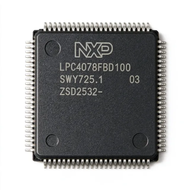
LPC4078FBD100 - 120MHz Cortex-M4 MCU 512KB Flash | NXP
LPC4078FBD100

LPC4078FBD100 - 120MHz Cortex-M4 MCU 512KB Flash | NXP

The NXP LPC4078FBD100 is an ARM Cortex-M4 based 32-bit digital signal controller for embedded applications requiring a high level of integration and low power dissipation, delivering 120MHz core performance with 512KB of on-chip flash in a 100-pin LQFP package. Key headline parameters are 120MHz ARM Cortex-M4 core, 512KB flash, 100-LQFP (14x14 mm). An ARM Cortex-M4 microcontroller is a 32-bit RISC processor core designed by ARM Holdings that combines microcontroller control features with digital signal processing (DSP) capabilities. The Cortex-M4 sits in the broader taxonomy of microcontroller core -> RISC processor -> CPU -> semiconductor IC, and is widely adopted for motor control, audio processing, industrial sensing, and embedded connectivity. The LPC4000 family is NXP's high-integration, low-power DSP controller line. Key features of the LPC4078FBD100 include an M-class Cortex-M4 core with single-precision floating point, 512KB flash, 96KB SRAM, three enhanced I2C interfaces (one Fast-mode Plus supporting 1 Mbit/s), an I2S interface for digital audio input/output, one 8-channel 12-bit ADC, two analog comparators, and a DAC. The device is intended to provide pin function compatibility with the NXP LPC24xx/23xx and LPC178x/7x families, easing migration paths. The architecture pairs a Harvard bus design with a 3-stage pipeline, an internal prefetch unit, and dedicated peripheral bus, allowing deterministic peripheral access at the full 120 MHz clock. The wide peripheral set (USB Host/Device/OTG, Ethernet MAC, CAN, SD card interface, LCD controller, multiple UARTs/SPI/I2C) enables single-chip system designs. Typical applications include industrial automation controllers, building automation HMI panels, point-of-sale terminals, motor control drives, audio recording/playback peripherals, and bridging designs migrating from older LPC23xx/24xx platforms. Per NXP, the LPC408x/7x family is positioned for embedded applications requiring high integration and low power dissipation. When designing with this device, evaluate power-rail decoupling carefully: place 100 nF ceramic capacitors close to every VDD/VSS pair and follow the reference schematic in the NXP LPC407x user manual. Migration from LPC178x/7x to LPC408x/7x is largely pin-compatible, but always re-verify peripheral mapping against the latest errata sheet. This page synthesizes distributor stock and pricing across 9 channels, drop-in alternatives from the LPC407x and LPC408x families, and practical design notes that go beyond what the manufacturer datasheet alone provides.

USD $7.38 स्टॉक में
LPC4078FET208 - 32-bit Arm Cortex-M4 MCU, 512KB Flash | NXP
LPC4078FET208

LPC4078FET208 - 32-bit Arm Cortex-M4 MCU, 512KB Flash | NXP

The NXP LPC4078FET208 is a 32-bit Arm Cortex-M4 digital signal controller for embedded applications requiring high integration and low power dissipation, housed in a 208-pin TFBGA (15x15 mm) package with 512 KB of on-chip Flash and up to 96 KB SRAM. It operates at up to 120 MHz core frequency with a single FPU and DSP extensions, plus an M0 coprocessor for low-latency I/O handling. A microcontroller (MCU) is a single-chip computer containing a CPU core, program and data memory, and a rich set of on-chip peripherals such as timers, communication interfaces, and analog blocks. Arm Cortex-M4 microcontrollers target deterministic real-time control and signal processing, occupying the mid-performance tier between Cortex-M0/M3 microcontrollers and Cortex-M7 high-end parts. The LPC407x family extends the Cortex-M4 lineage with NXP's familiar LPC peripheral set (EMC, Ethernet, USB, CAN, SPIFI) aimed at industrial communication, motor control, and human-machine interface designs. Key features include 512 KB Flash with in-system programming, 96 KB SRAM plus 4 KB EEPROM emulation, a 10/100 Ethernet MAC, two USB 2.0 controllers (Host/Device/OTG and Device/Host), two CAN 2.0B controllers, four UARTs, three enhanced I2C-bus interfaces (one Fast-mode Plus up to 1 Mbit/s), three SSP/SPI controllers, an I2S audio interface, an external memory controller (EMC) supporting SRAM, NOR Flash, and SDRAM, and a Quad-SPI Flash Interface (SPIFI) for high-speed off-chip code execution. An 8-channel 10-bit ADC and a 10-bit DAC support mixed-signal feedback, while four timers plus a PWM/Motor Control PWM unit handle power-conversion and motor drive tasks. The part supports 1.8 V to 3.6 V single-supply operation with brownout detect and on-chip power profiles. The architecture combines the Cortex-M4 main core with an Arm Cortex-M0 coprocessor that offloads I/O servicing through shared peripherals, reducing interrupt latency for time-critical peripherals such as Ethernet, USB, and CAN. The 4 KB EEPROM and 96 KB SRAM are large enough to host full TCP/IP stacks, USB device classes, and graphical user interface libraries without external memory; the EMC and SPIFI extend code space if needed. JTAG, SWD, and the on-chip ROM bootloader (UART, USB, SPI) cover in-field firmware updates. Typical applications include industrial Ethernet gateways, motor control (BLDC and stepper drives), building automation and HVAC controllers, point-of-sale terminals, USB peripherals, and human-machine interface panels with TFT LCD support. The 208-ball TFBGA exposes a wide external bus and the full peripheral set, fitting designs that need Ethernet plus USB plus CAN in one package. When designing with this part, allocate decoupling capacitors near each VDD/VSS pair and keep the TFBGA break-out on inner layers for signal integrity. Plan the boot mode straps (ISP, USB-CRC for the 4078/4088 parts) carefully if your firmware will boot from external SPIFI rather than internal flash. Use NXP's LPC407x CMSIS-pack and the LPCXpresso / MCUXpresso IDE for driver support and example peripheral initialization. This page synthesizes distributor pricing, drop-in alternative candidates, and practical design notes not found in a single manufacturer datasheet, providing an engineer-ready overview of the LPC4078FET208 in seconds.

RFQ संपर्क
LPC4088FBD144 - ARM Cortex-M4 MCU 120MHz 512KB | NXP
LPC4088FBD144

LPC4088FBD144 - ARM Cortex-M4 MCU 120MHz 512KB | NXP

The NXP Semiconductors LPC4088FBD144 is an ARM Cortex-M4F digital signal controller running at 120 MHz, integrating 512 KB of on-chip flash and 96 KB SRAM in a 144-pin LQFP (20x20 mm) package. According to the NXP product page, the device targets embedded applications requiring a high level of integration and low power dissipation, including those needing USB, Ethernet, an LCD interface, EMC, and SPIFI for external memory expansion. An ARM Cortex-M4 microcontroller is a 32-bit RISC processor core designed for deterministic embedded control, featuring a single-precision floating-point unit, DSP extensions via SIMD instructions, a Nested Vectored Interrupt Controller, and tightly-coupled memory for low-latency code execution. Within the broader taxonomy, the LPC4088 belongs to the Cortex-M4 family -> ARM Cortex-M -> 32-bit MCU -> microcontroller -> embedded processor -> semiconductor. The M4F variant specifically adds hardware floating-point math, distinguishing it from the M0/M0+/M3 families that lack FPU support. Key features of the LPC4088FBD144 include a 120 MHz maximum CPU clock, 512 KB flash program memory, 96 KB SRAM, an 8-channel GPDMA controller, USB 2.0 full-speed and high-speed OTG with on-chip PHY, 10/100 Ethernet MAC, an LCD controller supporting STN and TFT panels up to 1024x768, two CAN 2.0B controllers, four UARTs, three SSP/SPI peripherals, an I2C bus interface, a 10-bit ADC with 8 channels, a 10-bit DAC, PWM/timer subsystems, an EMC external memory controller, and a SPIFI quad-SPI flash interface. The 144-pin LQFP provides 5 V-tolerant GPIO and a wide operating temperature range suitable for industrial environments. Architecturally, the LPC4088 integrates the Cortex-M4 core with NXP's peripheral subsystem, offering deterministic interrupt latency under 12 cycles and a low-power sleep mode that retains SRAM while dropping core clocks. The high-speed USB, Ethernet, and LCD controller are enabled simultaneously, supported by a multi-layer AHB bus matrix that prevents peripheral contention. Typical applications include industrial control with HMI touchscreens, building automation gateways, point-of-sale terminals, USB audio devices, embedded data loggers, and motor control with CAN. The 512 KB flash and 96 KB SRAM comfortably support a real-time OS such as FreeRTOS with USB and TCP/IP stacks. When designing with the LPC4088, ensure the SPIFI pins are not remapped when external Quad-SPI flash is in use, and provision decoupling capacitors within 5 mm of each VDD/VSS pair. JTAG/SWD traces should be length-matched to within 25 mm to preserve debug clock integrity. This page synthesizes distributor pricing, drop-in alternatives, and practical design notes not found on a single distributor listing, helping engineers compare the LPC4088 against same-package NXP variants and cross-brand Cortex-M4 replacements.

RFQ संपर्क
LPC4310FET100 - Dual-Core 204 MHz MCU with USB | NXP
LPC4310FET100

LPC4310FET100 - Dual-Core 204 MHz MCU with USB | NXP

The NXP Semiconductors LPC4310FET100 is a 32-bit Arm Cortex-M4/M0 digital signal controller with up to 204 MHz processing performance, up to 264 kB of SRAM, Ethernet, two high-speed USB interfaces, and advanced configurable peripherals, housed in a 100-TFBGA package. It operates from a 2.2 V to 3.6 V supply and provides 83 I/O ports according to the supplied distributor data. A digital signal controller is a microcontroller architecture optimized for real-time control, communications, and signal-processing workloads. Within the embedded-semiconductor hierarchy, the LPC4310 combines an Arm Cortex-M4 main processor with an Arm Cortex-M0 coprocessor: the Cortex-M4 handles demanding control and DSP tasks, while the Cortex-M0 can manage independent peripheral operations. This division can reduce main-core interruption overhead in tightly timed systems. Key verified features include a 32-bit data bus, dual-core Arm Cortex-M4/M0 processing, up to 264 kB SRAM, Ethernet connectivity, and two high-speed USB ports. The 100-TFBGA package supports a high pin count in a compact 9 x 9 mm footprint, although its fine pitch requires careful PCB layout, assembly inspection, and multilayer board construction. The device targets embedded applications requiring signal processing and connected control. Its combination of Ethernet and dual USB connectivity makes it relevant to industrial gateways, data-acquisition controllers, USB-to-Ethernet bridges, and networked embedded monitoring systems. Its exact flash-memory organization, peripheral pin assignments, and operating-temperature limits were not supplied in the verified dataset and should be confirmed from NXP's technical documentation before design release. A key integration consideration is firmware partitioning between the two Arm cores. Developers should define ownership and synchronization rules for shared memory, interrupts, clocks, DMA channels, and peripherals early in the architecture. Firmware migration also requires validating startup code, linker placement, device drivers, and boot behavior rather than assuming that a higher-speed MCU is automatically software-compatible with another device. For a new design, verify the exact package ball map, external component requirements, Ethernet PHY interface, USB routing, and power sequencing against the official NXP documentation. Because the LPC4310FET100 is ROMless according to the distributor result, its application also depends on a suitable external program-memory implementation where required by the selected system configuration. This product page consolidates verified supplier information, package constraints, application guidance, and procurement data that are not normally presented together in a distributor listing. It also distinguishes verified facts from parameters that remain unavailable, helping engineers assess fit before requesting a quote or committing to PCB fabrication.

RFQ संपर्क
LPC4312JBD144E - 204MHz Dual-Core MCU | NXP | LQFP-144
LPC4312JBD144E

LPC4312JBD144E - 204MHz Dual-Core MCU | NXP | LQFP-144

NXP Semiconductors LPC4312JBD144E is a dual-core 32-bit Arm Cortex-M4/M0 microcontroller operating at up to 204 MHz, with 512 kB of flash and 136 kB of SRAM in a 144-pin LQFP package. It combines a high-performance Cortex-M4 core with a Cortex-M0 coprocessor and integrates Ethernet, two high-speed USB interfaces, LCD support, EMC peripherals, a quad SPI Flash Interface, and configurable timer and serial GPIO resources. A microcontroller is a programmable semiconductor that integrates a processor core, memory, and peripherals into one device for embedded control. The Cortex-M4 main core handles application code, networking, and USB tasks, while the Cortex-M0 coprocessor can execute dedicated control or peripheral-service routines. Within the device hierarchy, the LPC4312JBD144E is an Arm Cortex-M4/M0 MCU, an embedded microcontroller, and a member of the NXP LPC4300 family of 32-bit embedded processors. The 204 MHz Cortex-M4 core supports demanding embedded workloads, while the 512 kB flash provides nonvolatile program storage and the 136 kB SRAM supports working data, Ethernet buffers, display interfaces, and USB communications. Dual high-speed USB controllers are useful for systems requiring multiple USB device or host functions, while Ethernet supports connected industrial, communications, and control products. The integrated LCD and EMC resources reduce the need for some external peripherals. The LPC4300 family adds a Cortex-M0 coprocessor to the Cortex-M4 architecture. This arrangement allows the main core and coprocessor to execute separate tasks, which can improve responsiveness in interrupt-driven systems. The quad SPI Flash Interface provides a dedicated route to external serial flash for firmware expansion, graphics assets, data logging, or configuration storage. The State Configurable Timer and Serial General Purpose I/O interface extend timer and signal-routing flexibility for industrial and communications equipment. Typical applications include Ethernet-connected industrial controllers, USB-to-Ethernet data acquisition equipment, human-machine interface systems with LCD displays, communications infrastructure, and embedded gateways. The 144-pin LQFP package provides access to a broad set of high-speed and general-purpose I/O while remaining compatible with conventional board-assembly and inspection processes. Designers should verify clock, power, decoupling, USB, Ethernet, and display requirements against the manufacturer datasheet and user reference manual. The dual-core architecture also requires careful startup and interrupt-vector configuration so the main processor and coprocessor operate in the intended sequence. PCB layout should preserve short high-speed traces and provide appropriate return paths beneath Ethernet and USB interfaces. This product page combines exact NXP family and device specifications with package information, application guidance, comparison points, and drop-in alternatives identified from technical cross-references. It is intended to help engineers evaluate processor performance, memory capacity, peripheral integration, and PCB reuse before selecting the LPC4312JBD144E for an embedded design.

RFQ संपर्क
LPC4312JET100E - 204MHz Dual-Core MCU | NXP | 100-TFBGA
LPC4312JET100E

LPC4312JET100E - 204MHz Dual-Core MCU | NXP | 100-TFBGA

The NXP Semiconductors LPC4312JET100E is a 32-bit dual-core embedded microcontroller based on an Arm Cortex-M4 processor with an Arm Cortex-M0 coprocessor, operating up to 204 MHz and providing 512 KB of flash memory and 136 KB of on-chip SRAM in a 100-TFBGA package measuring 9 mm by 9 mm. The part also includes an Ethernet controller, two high-speed USB interfaces, LCD support, and a quad SPI Flash Interface for embedded applications requiring extensive connectivity. A microcontroller is an integrated circuit that combines a processor core, memory, peripherals, and communication interfaces on one semiconductor device. The LPC43xx family belongs to the Arm Cortex-M microcontroller hierarchy, where the Cortex-M4 core handles primary control and signal-processing tasks while the Cortex-M0 coprocessor can offload suitable background tasks. Ethernet, high-speed USB, LCD, and SPI Flash connectivity place the device between a general-purpose microcontroller and a more highly integrated communications processor. The verified product information identifies a 512 KB flash configuration, 136 KB of on-chip SRAM, and 16 KB of EEPROM for the LPC435x/3x/2x/1x family. Its quad SPI Flash Interface supports external serial-memory expansion, while Ethernet and two high-speed USB interfaces reduce the need for separate communication controllers. The 100-TFBGA package provides 100 terminals on a compact 9 mm by 9 mm surface-mount footprint suitable for compact industrial and communications equipment. The device combines a 204 MHz Cortex-M4 core with a Cortex-M0 coprocessor in one package. This heterogeneous arrangement can separate interrupt-intensive or peripheral-oriented work from the main control loop without requiring a second discrete microcontroller. Exact core frequencies, cache organization, and coprocessor performance allocation are not included in the supplied verified data, so those details should be confirmed in the manufacturer documentation before workload partitioning is finalized. Typical uses include industrial Ethernet equipment, USB-enabled embedded controllers, human-machine-interface systems with LCD connectivity, and designs requiring external SPI Flash storage. The Ethernet controller and dual high-speed USB support are particularly useful for connected data-acquisition, communications, and monitoring products. A design can also use the quad SPI Flash Interface to retain firmware, configuration, logs, or graphical assets outside the internal 512 KB flash. PCB planning must account for the fine-pitch 100-TFBGA land pattern, multilayer escape routing, power and ground distribution, and thermal management. Firmware selection should also verify boot, memory-map, peripheral, pin-muxing, and debugger requirements rather than assuming that software built for another LPC43xx member is interchangeable. Exact operating-temperature, voltage, and package-performance limits were not supplied and require confirmation from the NXP datasheet. This product record combines verified manufacturer and distributor information, an explicit treatment of missing electrical data, connectivity-focused application guidance, and pin-compatible same-family alternatives. It is intended to support engineering selection and sourcing decisions without presenting unverified specifications as guaranteed production facts.

RFQ संपर्क
LPC4313JBD144E - Dual-Core 204 MHz MCU | NXP | Industrial
LPC4313JBD144E

LPC4313JBD144E - Dual-Core 204 MHz MCU | NXP | Industrial

The NXP Semiconductors LPC4313JBD144E is a dual-core 32-bit microcontroller combining an Arm Cortex-M4 processor and an Arm Cortex-M0 coprocessor at up to 204 MHz, with 512 KB of flash memory and 136 kB of SRAM in a 144-LQFP package. The device also includes Ethernet, two high-speed USB interfaces, LCD support, and a broad collection of configurable peripherals for connected embedded systems. An Arm Cortex-M4/M0 microcontroller is an embedded processor architecture that pairs a high-performance Cortex-M4 core with a lower-power Cortex-M0 coprocessor. Within the product hierarchy, the LPC4313JBD144E belongs to the LPC4300 microcontroller family, combines real-time control with communications processing, and falls under the broader categories of embedded processors, 32-bit microcontrollers, and semiconductor devices. The principal features verified for this device include a 204 MHz operating frequency, 512 KB of internal flash, 136 kB of on-chip SRAM, 16 kB of EEPROM, Ethernet, two high-speed USB interfaces, LCD connectivity, and an Arm Cortex-M0 coprocessor. These resources support firmware-intensive control systems, human-machine interfaces, data acquisition, and USB- or Ethernet-connected equipment without requiring external flash for typical application firmware. Architecturally, the Cortex-M4 core handles the main real-time workload while the Cortex-M0 coprocessor can execute independent peripheral-control or monitoring tasks. The LPC4300 family includes the State Configurable Timer, Serial General Purpose I/O interface, and quad SPI Flash Interface, allowing designers to combine conventional fixed peripherals with event-based timing and serial GPIO functions. Typical uses include industrial Ethernet controllers, USB-to-Ethernet gateways, programmable automation equipment, medical monitoring systems, LCD-based human-machine interfaces, and embedded data-logging platforms. Its 144-LQFP package provides a large pin count for simultaneous Ethernet, USB, display, timer, and serial connectivity requirements. The primary design consideration is PCB and firmware complexity: a 144-pin LQFP requires careful escape routing, while Ethernet and USB interfaces require compliant layout, controlled-clock planning, correct termination, and validated signal integrity. Software must also reserve and initialize the M4 and M0 cores according to the manufacturer startup procedure. This page consolidates verified distributor and manufacturer information, distinguishes the directly identified same-package LPC4312JBD144E alternative, and provides application guidance and design cautions beyond a basic distributor listing. Availability, lifecycle status, and detailed electrical limits should be confirmed against current NXP documentation before production release.

RFQ संपर्क
LPC4313JET100E - Dual-Core 204 MHz MCU | NXP
LPC4313JET100E

LPC4313JET100E - Dual-Core 204 MHz MCU | NXP

NXP Semiconductors LPC4313JET100E is a 32-bit dual-core Arm Cortex-M4/M0 microcontroller with a 204 MHz processor, 512 KB of embedded flash, 136 KB of SRAM, Ethernet, two high-speed USB interfaces, LCD support, and EMC in a 100-ball TFBGA package measuring 9 mm by 9 mm. The Cortex-M4 core handles performance-intensive processing while the energy-efficient Cortex-M0 coprocessor supports control-oriented workloads. A microcontroller is a programmable integrated circuit containing a processor core, memory, and peripherals on one package. In the embedded-device hierarchy, the LPC4313JET100E belongs to the Arm Cortex-M MCU family and combines general-purpose control, communications connectivity, and real-time peripheral support. Its dual-core architecture can separate application code, communications handling, and background tasks without requiring a separate controller. The NXP product page highlights 512 KB of flash, 136 KB of SRAM, Ethernet, two high-speed USB ports, LCD connectivity, and EMC features. The Cortex-M0 coprocessor is code- and tool-compatible upward with the Cortex-M4 core and can reach 204 MHz, making it useful for transferring selected tasks away from the main core. The family also includes configurable timers, SGPIO, and a quad SPI Flash Interface for external memory and storage expansion. The LPC43xx architecture is designed for embedded systems requiring more connectivity and parallel processing than a basic microcontroller. Ethernet and dual high-speed USB support reduce the need for external communication controllers in gateways, industrial equipment, human-machine interfaces, and connected control systems. The 100-ball TFBGA-100 package also supports dense routing of the high-speed and display interfaces, although its fine pitch requires careful PCB layout and inspection. Typical applications include industrial Ethernet controllers, USB-connected data acquisition equipment, human-machine interface panels, communications gateways, and embedded motor-control systems. The principal design advantage is flexible workload allocation between the Cortex-M4 and Cortex-M0 cores, while the principal integration challenge is laying out a 9 mm by 9 mm ball-grid-array footprint with controlled power, clock, and high-speed signal routing. Use the NXP pin-description table and reference schematic when assigning PCB tracks and power domains. Place decoupling capacitors close to the supply balls, route Ethernet and USB differential pairs as controlled-impedance nets, and validate the Cortex-M4 and Cortex-M0 clock, reset, and boot configuration before committing the layout. This page consolidates the key NXP product characteristics, drop-in family alternatives, application guidance, package considerations, and design checks needed to evaluate the LPC4313JET100E for an embedded system.

RFQ संपर्क
LPC4315JBD144E - Dual-Core 204MHz ARM MCU | NXP
LPC4315JBD144E

LPC4315JBD144E - Dual-Core 204MHz ARM MCU | NXP

NXP Semiconductors LPC4315JBD144E is a 32-bit dual-core microcontroller built around an Arm Cortex-M4 processor operating up to 204 MHz with an Arm Cortex-M0 coprocessor. The device provides 768 KB of flash memory and is packaged in a 144-pin LQFP measuring 20 mm by 20 mm. Its combination of Ethernet, two high-speed USB interfaces, LCD support, and configurable peripherals targets industrial embedded systems that require substantial connectivity and real-time control in one device. An Arm Cortex-M4/M0 microcontroller is a type of 32-bit microcontroller, itself part of the embedded processor and embedded systems hierarchy. The Cortex-M4 core handles performance-oriented control, communications, and signal-processing tasks, while the Cortex-M0 coprocessor can service peripheral operations independently. This division can reduce interrupt-related load on the primary core and supports deterministic multi-peripheral designs without requiring a separate controller. The LPC4315JBD144E combines 768 KB of flash with the LPC43x family capacity of up to 1 MB, 136 kB of on-chip SRAM, and 16 kB of EEPROM. Peripherals include Ethernet, two high-speed USB ports, an LCD interface, a quad SPI Flash Interface, the State Configurable Timer, and Serial General Purpose I/O. These resources make the microcontroller suitable for gateways, human-machine interfaces, data acquisition equipment, and connected industrial controllers. The dual-core architecture provides a practical way to partition control and communication workloads. The primary Cortex-M4 core can execute application logic and higher-bandwidth network routines, while the Cortex-M0 core can handle auxiliary I/O or peripheral tasks. The exact clock, voltage, timing, peripheral-enable, and temperature details for each device variant must be confirmed in the NXP manufacturer datasheet before final firmware and hardware configuration. Typical uses include Ethernet-connected industrial equipment, USB-to-serial data acquisition systems, LCD-equipped operator panels, SPI Flash update systems, and embedded gateways. The 144-LQFP package exposes substantially more I/O than smaller microcontroller packages, making the device appropriate for designs requiring multiple buses, parallel LCD data, Ethernet connectivity, and USB host or device functions. Designers should allocate the pin multiplexing, clocks, power rails, and boot options from the device-specific pin table before PCB routing. Firmware must also account for separate Cortex-M4 and Cortex-M0 startup and peripheral ownership. Use the manufacturer datasheet for the exact pin names and boot configuration, and validate the PCB against the selected package and revision. This product page combines the manufacturer overview, distributor identification, package information, application guidance, and same-family replacement analysis into an engineering-focused reference. It highlights the role of the Cortex-M4/M0 architecture, memory resources, connectivity peripherals, PCB considerations, and qualification steps that raw distributor listings do not explain.

RFQ संपर्क