उत्पाद (19,000+)

STM8S207K6T6 - 24MHz 8-bit MCU, 32KB Flash | STMicroelectronics
STM8S207K6T6

STM8S207K6T6 - 24MHz 8-bit MCU, 32KB Flash | STMicroelectronics

The STM8S207K6T6 is a performance-line 8-bit microcontroller from STMicroelectronics, featuring a 24 MHz STM8 core with up to 32 Kbytes of Flash program memory. It integrates 2 Kbytes of data EEPROM, a 10-bit ADC, multiple timers, two UARTs, SPI, I²C, and CAN interfaces, all in a 32-pin LQFP package. This MCU is designed for cost-sensitive industrial and consumer applications requiring robust communication and control capabilities. An 8-bit microcontroller (MCU) is a single-chip computer with an 8-bit data bus, executing instructions on 8-bit words. It integrates a CPU, memory (Flash, RAM, EEPROM), and peripherals (timers, ADC, communication interfaces) on one die. In the system hierarchy, an 8-bit MCU sits below 16-bit and 32-bit MCUs in processing power but offers lower cost, simpler architecture, and lower power consumption, making it ideal for control-oriented tasks like motor control, sensor interfacing, and human-machine interfaces. The STM8S207K6T6 belongs to the STM8S20xxx performance line, which balances performance and peripheral richness for mid-range embedded applications. Key features include a 24 MHz CPU clock, 32 Kbytes of Flash, 2 Kbytes of RAM, 2 Kbytes of EEPROM, a 10-bit ADC with up to 10 channels, two 16-bit timers, one 8-bit timer, two UARTs, SPI, I²C, and a CAN 2.0B controller. The device operates from 2.95V to 5.5V, making it suitable for 3.3V and 5V systems. It also features a low-power mode with typical current consumption of 5.4 mA at 24 MHz, and a halt mode with 1.5 µA typical current. The STM8S207K6T6 uses a Harvard architecture with a 3-stage pipeline, achieving up to 20 MIPS at 24 MHz. It includes an embedded debug module (SWIM) for in-circuit debugging and programming, and a single-wire interface for firmware updates. The CAN controller supports CAN 2.0B active mode, enabling robust industrial networking. The device is manufactured using ST's proprietary 130nm process, balancing performance and power efficiency. Typical applications include industrial control systems, home appliances, automotive body electronics (non-safety), sensor nodes, and communication gateways. The CAN interface makes it particularly suitable for automotive and industrial CAN bus networks, while the multiple UARTs and SPI/I²C support diverse peripheral connectivity. When designing with this MCU, ensure proper decoupling of the VDD and VDDA pins with 100nF capacitors placed close to the pins. The SWIM pin should be pulled up with a 10kΩ resistor for reliable programming. For CAN applications, an external CAN transceiver (e.g., TJA1050) is required, and the bus termination resistor should be 120Ω at each end of the CAN bus.

RFQ संपर्क
STM8S207R6T6 - 24MHz 8-Bit MCU 32KB Flash LQFP-64 | STMicroelectronics
STM8S207R6T6

STM8S207R6T6 - 24MHz 8-Bit MCU 32KB Flash LQFP-64 | STMicroelectronics

The STMicroelectronics STM8S207R6T6 is a performance-line 8-bit STM8S microcontroller built around a CISC Harvard architecture core running at 24 MHz (20 MIPS) with 32 KB of on-chip Flash program memory and up to 2 KB of SRAM plus an integrated EEPROM data area. It integrates a 10-bit ADC, two 16-bit timers plus one 8-bit timer, two UARTs, SPI, I2C, and CAN, all in a 64-pin LQFP (T6 suffix) package operating from 2.95 V to 5.5 V. The device is positioned in the STM8S20xxx family which scales from 32 KB to 128 KB Flash and is intended for cost-sensitive motor-control, appliance, and industrial-control applications. An 8-bit microcontroller (MCU) is a single-chip computer that integrates a CPU, non-volatile program memory, working RAM, and peripherals onto one silicon die. The STM8 family uses a CISC 8-bit core with a 16-bit instruction word, giving higher code density than legacy 8051 cores while retaining the predictable interrupt latency and deterministic timing that embedded control designers prefer. The STM8S207 series specifically belongs to the STM8S "performance line," sitting above the access-line STM8S103 and below the value-line STM8S105, and is paired with ST's Cosmic, IAR, and Raisonance toolchains plus the free STVD development environment. Key features of the STM8S207R6T6 include a 20 MIPS peak instruction throughput at 24 MHz, integrated CAN 2.0B interface, a 1 Mbyte linear address space, a single-wire SWIM debug interface, and an embedded bootloader stored in ROM for in-application Flash programming. The device offers 38 GPIOs with 5 V tolerance on most pins and supports up to 16 external interrupts. Watchdog, auto-wakeup, and a 4-level low-power run/wait/slow/halt scheme allow the device to drop quiescent current below 5 uA in Halt with full RAM retention. Architecturally, the STM8S core pairs a 32-bit program address bus with a 24-bit data address bus and supports up to 16 Mbytes of linear addressing for data, while code is read from a separate Flash bus. This Harvard split removes fetch-decode stalls that plague older 8-bit Von Neumann designs and is the reason the family reaches 20 MIPS at 24 MHz without wait states. A 32 KB Flash variant such as the STM8S207R6 sits at the low-memory end of the family, sharing the same peripheral set as the larger 64 KB (R8) and 128 KB (RB) siblings. Typical applications include BLDC/PMSM motor control in appliances, HVAC fan and pump control, smart metering, lighting ballast control, industrial sensor hubs, and CAN-connected remote I/O nodes. The integrated CAN controller, combined with 32 KB Flash, makes the part a good fit for distributed industrial nodes that need deterministic on-chip comms without an external transceiver MCU. When designing with the STM8S207R6T6, pay attention to the 5 V I/O tolerance (most pins are true 5 V tolerant, but a few high-current pins are FT-compat only) and to the SWIM pin shared with NRST; the debug probe needs a tri-state buffer on the SWIM line for in-circuit debugging without disabling reset. The internal 16 MHz HSI RC is accurate to about 1 percent after user trimming, but designs that need CAN bit-time accuracy must select the external HSE crystal option. This page synthesizes distributor pricing, drop-in LQFP-64 alternatives, and practical hardware design notes not found in the manufacturer datasheet alone.

RFQ संपर्क
STM8S207RBT6 - 24MHz 128KB 8-Bit MCU | STMicroelectronics
STM8S207RBT6

STM8S207RBT6 - 24MHz 128KB 8-Bit MCU | STMicroelectronics

The STMicroelectronics STM8S207RBT6 is an 8-bit STM8S performance-line microcontroller with a 24 MHz maximum CPU frequency, 128 KB of Flash program memory, 20 MIPS performance, and a 64-pin LQFP package measuring 10 x 10 mm. It is designed for embedded control applications requiring integrated communications, mixed-signal measurement, and broad peripheral support. An 8-bit microcontroller is a compact embedded computing device that executes firmware from nonvolatile Flash memory while using timers, serial interfaces, and analog inputs to control a target system. The STM8S207RBT6 belongs to the STM8S performance-line hierarchy of 8-bit RISC microcontrollers, combining an advanced Harvard-architecture core with integrated EEPROM, analog, timing, and communication peripherals. Key features include a maximum CPU frequency of 24 MHz, 128 KB of Flash, a three-stage pipeline, a 10-bit ADC, two UARTs, SPI, I2C, and CAN connectivity. According to the STM8S207RBT6 product information, these peripherals allow the device to consolidate functions that would otherwise require separate interface and conversion ICs. The LQFP-64 package also provides numerous general-purpose I/O pins for external sensing, actuation, and communication connections. The STM8 core uses Harvard architecture, separating instruction and data access paths, while the three-stage pipeline supports efficient instruction throughput. At the maximum 24 MHz operating frequency, the device delivers up to 20 MIPS. Integrated EEPROM supports parameter and configuration storage, although its exact capacity must be confirmed from the complete manufacturer datasheet before it is reserved in firmware. Typical applications include industrial controllers, motor-control and automation equipment, communication modules, building-control interfaces, consumer appliances, and compact embedded control panels. CAN, SPI, I2C, and UART support is particularly useful for systems that must connect sensors, actuators, human-interface modules, or service buses while retaining a compact embedded-control architecture. Designers should verify the complete 64-pin pinout, peripheral alternate-function mappings, clock configuration, and decoupling requirements against the manufacturer datasheet. The 10 x 10 mm LQFP footprint is easy to inspect after soldering, but its fine-pitch leads still require careful land-pattern and paste-volume control for reliable assembly. This product page consolidates verified manufacturer and distributor information, package details, sourcing data, application guidance, and temperature-grade replacement options into an engineering-focused reference. It distinguishes exact drop-in options from broader functional comparisons so designers can make a package- and pin-compatible selection without overlooking software or qualification constraints.

RFQ संपर्क
STM8S207S8T6 - 24MHz 8-bit MCU, 64KB Flash | STMicroelectronics
STM8S207S8T6

STM8S207S8T6 - 24MHz 8-bit MCU, 64KB Flash | STMicroelectronics

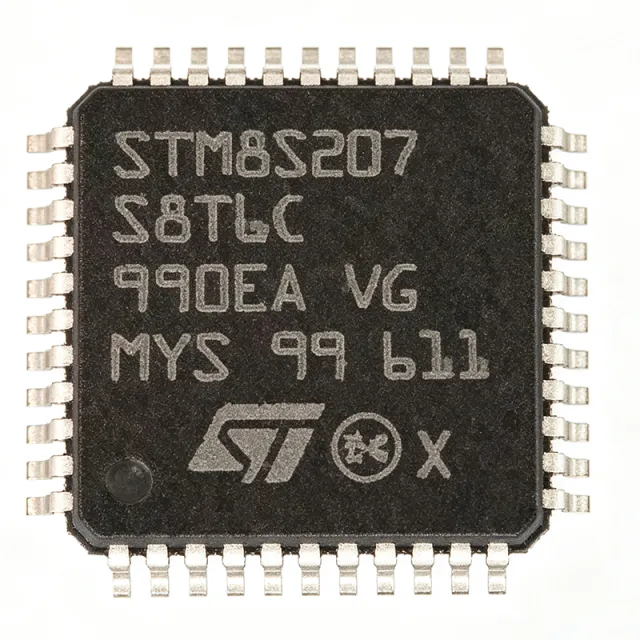
The STM8S207S8T6 is a performance-line 8-bit microcontroller from STMicroelectronics, operating at up to 24 MHz with 64 Kbytes of Flash program memory. It is part of the STM8S20xxx family, which offers from 32 to 128 Kbytes of Flash, and is housed in a 44-pin LQFP package. The device integrates a rich set of peripherals including a 10-bit ADC, multiple timers, two UARTs, SPI, I2C, and CAN, making it suitable for a wide range of industrial and consumer applications. An 8-bit microcontroller (MCU) is a single-chip computer with an 8-bit data bus, executing instructions on 8-bit words. It typically integrates a CPU core, memory (Flash, RAM, EEPROM), and programmable peripherals on a single die. In the system hierarchy, an 8-bit MCU sits below 16-bit and 32-bit counterparts in processing power but offers lower cost, simpler architecture, and adequate performance for control-oriented tasks. The STM8S207S8T6 belongs to the STM8S performance line, which is designed for applications requiring higher clock speeds and richer connectivity than the value line, while maintaining the ease of use and robustness of the STM8 core. Key features of the STM8S207S8T6 include a 24 MHz CPU clock, 64 KB of Flash memory, 2 KB of data EEPROM, and a 10-bit ADC with up to 16 multiplexed channels. It also provides two UARTs, one SPI, one I2C, and a CAN 2.0B interface, enabling flexible communication in industrial networks. The device operates from a 3.3V or 5V supply, with a wide operating temperature range of -40°C to +85°C, and is available in a 44-pin LQFP package with a 10x10 mm body and 0.8 mm pitch. Technically, the STM8S207S8T6 is built on a high-performance 8-bit core with a three-stage pipeline, achieving up to 20 MIPS at 24 MHz. It includes a nested interrupt controller, a clock controller with multiple sources (internal RC, external crystal, or PLL), and a comprehensive set of timers including a 16-bit advanced control timer, two 16-bit general-purpose timers, and an 8-bit basic timer. The device also features a CAN controller with 3 mailboxes, supporting both standard and extended identifiers, which is critical for automotive and industrial networking. Typical applications include industrial control systems, home appliances, power tools, and automotive body electronics. The CAN interface makes it particularly suitable for automotive networks, while the rich timer set and ADC support motor control and sensor interfacing. The 5V tolerance simplifies direct connection to legacy sensors and actuators without level shifting. When designing with this MCU, ensure proper decoupling of the VDD and VDDA pins with 100 nF capacitors placed close to the device. The internal RC oscillator can be used for cost-sensitive designs, but for precise timing, an external crystal is recommended. The STM8S207S8T6 supports in-circuit programming and debugging via the SWIM interface, which requires a single-wire connection and simplifies firmware updates.

USD $2.39 संपर्क
STM8S207SBT6C - 24MHz 8-bit MCU 128KB Flash LQFP-44 | STMicroelectronics
STM8S207SBT6C

STM8S207SBT6C - 24MHz 8-bit MCU 128KB Flash LQFP-44 | STMicroelectronics

The STMicroelectronics STM8S207SBT6C is a 24 MHz 8-bit STM8S microcontroller with 128 KB program Flash and integrated EEPROM, housed in a 44-pin LQFP package. As a member of the STM8S performance line, this part delivers up to 24 MIPS CPU throughput, integrates a 10-bit ADC, multiple 16-bit timers, two UARTs, SPI, I2C and CAN peripherals, and is rated for 3.0 V to 5.5 V single-supply operation. An 8-bit MCU (microcontroller unit) is a self-contained computing IC that integrates a CPU core, non-volatile program memory (Flash), read/write data memory (RAM/EEPROM), and configurable peripherals (ADC, timers, communication interfaces) on a single die. Within the broader semiconductor taxonomy, an MCU is a sub-category of microcontroller -> embedded processor -> semiconductor device. The STM8S family uses a Harvard-architecture CISC core designed for deterministic real-time control, balancing low power, high code density, and 5 V tolerance that simplifies interfacing to legacy analog and industrial peripherals. The STM8S207SBT6C's key specifications include 38 general-purpose I/O lines, a 10-bit successive-approximation ADC with up to 16 channels, a 1 KB true-EEPROM data area plus 6 KB user RAM, two UARTs (including LIN master capability), one SPI peripheral, one CAN 2.0B interface, and a beCAN controller. Integrated reset circuitry, internal 16 MHz RC oscillator, and window watchdog reduce external component count. The part supports up to 30 kV ESD HBM and operates across -40 °C to +85 °C. Architecturally the STM8S uses a modified Harvard layout, 32-bit program counter with 24-bit linear addressing, and a single-cycle 8x8 multiplier, providing efficient C code generation. The 5 V-tolerant GPIO eliminates level shifters when interfacing to legacy 5 V sensors and drivers, while the integrated CAN controller removes the need for an external transceiver controller. A flexible clock tree with internal 16 MHz HSI reduces external crystal cost for cost-sensitive designs. Typical applications include industrial sensor conditioning nodes, building automation controllers, smart metering peripherals, automotive body and chassis subsystems, low-end motor control boards, and white-goods user-interface modules. Designers choose this STM8S207 variant when 128 KB Flash headroom is needed for communication stacks (CANopen, Modbus) while staying inside the 5 V-tolerant 8-bit ecosystem. A critical design consideration is power budgeting: at 24 MHz the core draws roughly 10 mA plus peripheral contributions, so a clean 3.3 V or 5 V LDO rail is recommended. Decouple VDD/VSS pairs with 100 nF X7R ceramic capacitors placed within 3 mm of each pin pair, and reserve a 4.7 uF bulk capacitor on the main rail. The CAN bus requires a 120 ohm termination offset on each end and a common-mode choke for industrial EMC compliance. This page synthesizes distributor pricing, drop-in alternatives, and practical design notes not consolidated on the manufacturer datasheet or individual supplier listings.

RFQ संपर्क
STM8S208C6T6 - 24MHz 32KB Flash 8-Bit MCU | STMicroelectronics
STM8S208C6T6

STM8S208C6T6 - 24MHz 32KB Flash 8-Bit MCU | STMicroelectronics

STMicroelectronics STM8S208C6T6 is a 24 MHz, 8-bit STM8S performance-line microcontroller with 32 KB of Flash memory, 12 KB of RAM, and 6 KB of integrated EEPROM in a 48-LQFP 7 x 7 mm package. The device operates from 3 V to 5.5 V and provides 38 I/O ports for compact embedded control systems. A microcontroller is a semiconductor device that integrates a processor core, program memory, data memory, and peripherals on one chip. The STM8S208 belongs to the hierarchy of 8-bit microcontrollers, embedded controllers, and integrated circuits. It combines a high-performance 8-bit core with communication and timing resources suited to cost-sensitive industrial, consumer, communications, and appliance-control products. Key features include a 24 MHz maximum clock, 32 KB Flash organized as 32K x 8, 12 KB RAM, and a 10-bit ADC. Integrated peripherals include timers, two UARTs, SPI, I2C, and CAN. The 48-LQFP package provides 38 I/O pins, allowing a design to combine digital control with analog measurement and multiple serial interfaces without requiring a larger package. The STM8S208 platform is implemented around a high-performance 8-bit core and a peripheral set designed for embedded control. Its combination of 32 KB Flash and 12 KB RAM gives embedded firmware room for state-machine logic, communications routines, calibration data, and application control. The CAN interface is particularly useful for distributed equipment where a controller must exchange periodic data over a robust vehicle or industrial network. Typical applications include industrial controllers, communication modules, motor and appliance controls, instrumentation, CAN-connected equipment, and compact consumer products. For a CAN design, the MCU can handle local real-time control while the CAN peripheral manages framed network traffic. For instrumentation, the 10-bit ADC supports analog measurements, while UART, SPI, and I2C cover external sensors, displays, and configuration devices. Designers should verify the exact peripheral pin assignments, alternate-function multiplexing, clock configuration, decoupling requirements, and programming interface from the manufacturer datasheet before layout. The 3 V to 5.5 V operating range supports both 3.3 V and 5 V system rails, but each connected peripheral and external component must also tolerate the selected rail voltage. This page consolidates the verified 24 MHz, 32 KB Flash, 48-LQFP device information with same-family drop-in candidates, commercial purchasing guidance, and practical selection considerations that are not presented as one compact view in distributor listings.

RFQ संपर्क
STM8S208C8T6 - 8-Bit 24MHz MCU, 64KB Flash | STMicroelectronics
STM8S208C8T6

STM8S208C8T6 - 8-Bit 24MHz MCU, 64KB Flash | STMicroelectronics

The STM8S208C8T6 is a high-performance 8-bit microcontroller from STMicroelectronics, part of the STM8S Performance line. It operates at a maximum frequency of 24 MHz and features 64 KB of Flash memory, 2 KB of EEPROM, and 4 KB of RAM. The device is housed in a 48-pin LQFP package (7x7 mm) and supports a supply voltage range of 2.95V to 5.5V, making it suitable for a wide range of industrial and consumer applications. An 8-bit microcontroller (MCU) is a single-chip computer with an 8-bit central processing unit (CPU), memory, and peripherals. It is a type of embedded processor used to control electronic systems. In the hierarchy of computing devices, an 8-bit MCU is a subset of microcontrollers, which are a subset of embedded systems, which are a subset of electronic systems. The STM8S208C8T6 is a CISC (Complex Instruction Set Computer) architecture MCU, offering a rich instruction set and efficient code density. Key features of the STM8S208C8T6 include a 10-bit analog-to-digital converter (ADC) with up to 16 channels, multiple timers (including a 16-bit advanced control timer, a 16-bit general-purpose timer, and a basic timer), and a comprehensive set of communication interfaces: two UARTs, one SPI, one I2C, and one CAN interface. The device also includes an integrated EEPROM for data storage, a watchdog timer, and a low-power mode for energy-efficient operation. The STM8S208C8T6 is built on a high-performance 8-bit core with a three-stage pipeline, achieving up to 20 MIPS at 24 MHz. It features a flexible clock control with an internal RC oscillator, an external crystal oscillator, and a phase-locked loop (PLL) for frequency multiplication. The device supports in-circuit programming and debugging via the SWIM (Single Wire Interface Module) interface, simplifying firmware development and field updates. Typical applications include industrial control systems, home automation, consumer electronics, automotive body electronics, and power management. The CAN interface makes it particularly suitable for automotive and industrial networking applications where robust communication is required. The wide operating voltage range and low-power modes enable battery-powered and energy-harvesting designs. When designing with the STM8S208C8T6, ensure proper decoupling of the power supply pins with 100nF capacitors placed close to the VDD and VSS pins. The SWIM interface should be reserved for programming and debugging. For CAN applications, an external CAN transceiver (e.g., TJA1050) is required. The device is RoHS compliant and available in tray packaging.

RFQ संपर्क
STM8S208R8T6 - 8-Bit 24MHz 64KB Flash MCU | STMicroelectronics
STM8S208R8T6

STM8S208R8T6 - 8-Bit 24MHz 64KB Flash MCU | STMicroelectronics

The STM8S208R8T6 is a high-performance 8-bit microcontroller from STMicroelectronics' STM8S series, featuring a 24 MHz CPU core, 64KB of Flash program memory, and 6KB of RAM. It is housed in a 64-pin LQFP package (10x10 mm) and operates from a 3.3V or 5V supply, making it suitable for a wide range of industrial and consumer applications. An 8-bit microcontroller (MCU) is a single-chip computer with an 8-bit data bus, integrating a CPU, memory, and peripherals. The STM8S series is a family of 8-bit MCUs from STMicroelectronics, positioned between low-end 8-bit devices and 32-bit ARM-based MCUs. It offers a cost-effective solution for applications requiring moderate processing power, rich peripherals, and low power consumption. The STM8S208R8T6 belongs to the performance line, which provides higher clock speeds and more memory compared to access line devices. Key features include a 24 MHz maximum CPU frequency with 0 wait states, 64KB of Flash memory, 6KB of RAM, and 2KB of EEPROM. It integrates a 10-bit ADC with up to 16 channels, multiple 16-bit timers, two UARTs, SPI, I2C, and a CAN interface. The device also includes a watchdog timer, brown-out reset, and low-power modes, enhancing reliability and energy efficiency. The STM8S208R8T6 is built on ST's advanced 8-bit core architecture, which delivers up to 20 MIPS at 24 MHz. It features a Harvard architecture with separate instruction and data buses, allowing simultaneous instruction fetch and data access. The integrated EEPROM enables non-volatile data storage without external components, and the CAN interface supports robust communication in automotive and industrial networks. Typical applications include industrial control systems, home appliances, automotive body electronics, and communication modules. The CAN interface makes it ideal for automotive networks, while the rich timer and ADC peripherals suit motor control and sensor interfacing. The wide operating voltage range (2.95V to 5.5V) ensures compatibility with both 3.3V and 5V logic systems. When designing with this MCU, ensure proper decoupling of the power supply and a stable clock source. The device supports multiple clock sources, including an internal RC oscillator and external crystal. For low-power applications, utilize the halt and active-halt modes to reduce current consumption. The CAN interface requires an external transceiver, such as the TJA1050, for physical layer connectivity.

RFQ संपर्क
STM8S208RBT3 - 24MHz 128KB 8-Bit MCU | STMicroelectronics
STM8S208RBT3

STM8S208RBT3 - 24MHz 128KB 8-Bit MCU | STMicroelectronics

The STMicroelectronics STM8S208RBT3 is an 8-bit STM8S performance-line microcontroller with a 24 MHz CPU, 128 KB of Flash program memory, integrated EEPROM, a 10-bit ADC, and communication peripherals including two UARTs, SPI, I²C, and CAN. The device is supplied in a 64-LQFP package measuring 10 x 10 mm and is intended for compact embedded-control systems. An 8-bit microcontroller is a programmable semiconductor containing a processor core, memory, and integrated peripherals on one device. STM8 devices belong to the broader microcontroller and embedded-processor hierarchy, combining an 8-bit CISC-oriented architecture with deterministic real-time control peripherals. The STM8S208 performance line is positioned above smaller STM8 families by offering more Flash memory and a broad selection of communication and timing resources. Key features of the STM8S208RBT3 include operation at up to 24 MHz, 128 KB of Flash, integrated EEPROM, a 10-bit analog-to-digital converter, multiple timers, 38 I/O ports, and support for UART, SPI, I²C, and CAN communication. These resources allow the MCU to consolidate several discrete functions on a single device and reduce component count in industrial controls, communications equipment, access systems, and embedded measurement products. The STM8S architecture supports a supply range of 3 V to 5.5 V according to the verified distributor data. Its integrated EEPROM provides nonvolatile data storage without requiring an external memory chip, while the 10-bit ADC supports analog sensor acquisition. Two UART channels enable asynchronous serial connectivity, SPI supports higher-speed peripherals, I²C supports external sensors and EEPROMs, and CAN supports industrial network nodes. Typical applications include industrial automation controllers, CAN-connected equipment, motor and relay control, environmental monitoring, access-control terminals, serial data acquisition, and compact consumer appliances. The 64-LQFP package provides enough I/O for external sensors, displays, transceivers, and actuators while remaining practical for leaded PCB assembly and prototype development. Designers should verify the exact pin assignment, electrical limits, oscillator requirements, reset circuit, and decoupling recommendations against the STM8S208RB manufacturer documentation before layout. The 3 V to 5.5 V supply requirement means external interface levels and sensor voltages must remain compatible with the MCU pins used. This product page consolidates verified manufacturer and distributor specifications, same-package replacement guidance, interface coverage, and practical engineering considerations into one reference for engineers evaluating the STM8S208RBT3.

RFQ संपर्क
STM8S208RBT6 - 8-Bit 24MHz 128KB Flash MCU | STMicroelectronics
STM8S208RBT6

STM8S208RBT6 - 8-Bit 24MHz 128KB Flash MCU | STMicroelectronics

STMicroelectronics STM8S208RBT6 is an 8-bit STM8S performance-line microcontroller operating at 24MHz with 128KB of Flash program memory and up to 20MIPS throughput. It is supplied in a 64-pin LQFP package and supports 3.3V and 5V operation according to the verified product listings. Integrated peripherals include a 10-bit ADC, timers, two UARTs, SPI, I2C, and CAN. An STM8S microcontroller belongs to the 8-bit embedded-control segment of the semiconductor hierarchy. These devices combine a compact CISC core, embedded nonvolatile memory, analog conversion, serial communication, and timing peripherals in one package. They are used where deterministic control, low system complexity, and economical embedded intelligence are more important than the processing power and memory bandwidth of a 32-bit Cortex-M MCU. The STM8S208RBT6 combines 128KB Flash with a 24MHz clock, delivering 20MIPS as identified by Mouser. Its integrated 10-bit ADC supports measurements without a separate converter, while two UARTs, SPI, I2C, and CAN provide several paths for sensors, displays, industrial networks, and external controllers. This interface density makes the device suitable for compact industrial controllers, motor-control helpers, communication gateways, and embedded measurement products. As an STM8S20xxx performance-line part, the device belongs to a family offered from 32KB through 128KB Flash. The selected 128KB configuration provides more program space than lower-density variants while preserving the familiar STM8S peripheral and software environment. This supports protocol stacks, application logic, logging, and parameter handling in a single embedded controller. Typical applications include CAN-connected industrial nodes, sensor acquisition and control, motor or actuator supervision, and compact communication equipment. The CAN interface is valuable when the design must participate in a bus network, while the ADC and multiple serial interfaces support local sensing. Designers should still verify timing, peripheral availability, pin multiplexing, and memory requirements in the manufacturer documentation before finalizing firmware. The principal design consideration is that software compatibility does not guarantee an unconditional drop-in replacement. Firmware startup code, interrupt vectors, peripheral configuration, clock settings, and PCB pad assignments must all be checked. For new designs, the 128KB Flash capacity and broad mixed-signal connectivity can reduce external components, but the 64-pin LQFP footprint requires adequate board area and careful routing of analog and communication signals. This product page combines verified manufacturer, distributor, and cross-reference information with practical design guidance. It helps engineers assess the STM8S208RBT6, compare documented same-family options, understand its peripherals, and plan sourcing and PCB integration without presenting unsupported electrical values.

RFQ संपर्क
STM8S903F3M6 - 16MHz 8KB 8-Bit MCU | STMicroelectronics
STM8S903F3M6

STM8S903F3M6 - 16MHz 8KB 8-Bit MCU | STMicroelectronics

The STMicroelectronics STM8S903F3M6 is an 8-bit STM8S-series microcontroller operating at 16 MHz, with 8 KB of Flash memory, 16 I/O ports, and a 20-SOIC package. According to the verified distributor data, it is available in a 20-SO package and is identified as an active, RoHS-compliant device with a 2.95 V to 5.5 V supply-voltage range. What is an 8-bit microcontroller? An MCU is a semiconductor device that combines a processor core, program memory, data memory, and peripherals on one integrated circuit. The STM8S903F3M6 belongs to the 8-bit MCU -> embedded microcontroller -> semiconductor hierarchy and is intended for compact control, measurement, and communication systems where a dedicated processor, memory, and serial interfaces are required. Verified specifications identify 8 KB of Flash memory, 1 KB of RAM, 640 bytes of EEPROM, a 10-bit ADC, two timers, UART, SPI, and I²C. These peripherals make the device suitable for sensor acquisition, actuator control, industrial instrumentation, and low-cost embedded products. The 16 MHz clock provides the processing headroom needed for basic control loops and serial data handling, although the verified data does not specify the complete peripheral timing or ADC accuracy. The STM8S903F3M6 uses a 20-SOIC package, also described as a 0.295-inch, 7.50 mm-width SOP package in the verified distributor data. The SOIC outline is a surface-mount package with gull-wing leads, making it suitable for conventional PCB assembly and prototype-to-production transfer. The package pinout and exposed thermal-pad details are not included in the supplied verified data, so the pinout is reported as null rather than inferred. Typical applications include compact industrial controllers, low-power sensor nodes, simple motor or relay-control boards, data-acquisition modules, UART-to-digital bridges, and small SPI or I²C peripheral boards. The STM8 family can be paired with external sensors and communication transceivers, while the integrated ADC supports analog measurement. Final firmware support should be confirmed with the applicable STMicroelectronics development tools and device documentation. For PCB design, preserve the manufacturer's recommended decoupling and grounding layout, and verify all peripheral pins, reset behavior, clock requirements, and package dimensions against the official datasheet before production. This page combines verified distributor specifications, package data, sourcing information, and engineering-oriented application guidance without treating unverified details as guaranteed specifications.

RFQ संपर्क
STM8S903F3P6 - 16MHz 8-Bit MCU | STMicroelectronics
STM8S903F3P6

STM8S903F3P6 - 16MHz 8-Bit MCU | STMicroelectronics

STMicroelectronics STM8S903F3P6 is an 8-bit STM8S-series microcontroller operating at up to 16 MHz, with 8 KB of Flash program memory and a 20-TSSOP package. The device operates from 2.95 V to 5.5 V and provides 1 KB of RAM, 640 bytes of true EEPROM, a 10-bit ADC, two timers, UART, SPI, and I²C connectivity. It is designed for compact embedded-control systems requiring mixed analog and digital functions without a higher-cost 32-bit MCU. An 8-bit microcontroller is a programmable semiconductor containing a processor core, nonvolatile program memory, data memory, and integrated peripherals. Within the hierarchy of embedded semiconductors, an MCU is below a microprocessor in processing capability but combines greater control simplicity with lower system cost and power use. The STM8S903F3 belongs to STMicroelectronics’ STM8S access line and targets cost-sensitive consumer, appliance, and industrial-control applications. Key features include 8 KB of Flash, 1 KB of RAM, and 640 bytes of EEPROM, allowing firmware, working data, and nonvolatile parameters to be consolidated in one device. The 10-bit ADC supports analog measurement, while two timers support timing and periodic control functions. UART, SPI, and I²C interfaces cover serial communication, sensor connectivity, and expansion to external ICs. The 2.95 V to 5.5 V supply range accommodates both 3.3 V and 5 V system environments. The STM8S903F3 architecture combines an 8-bit STM8 core with dedicated peripheral resources and true data EEPROM. Its 16 MHz maximum clock rate provides sufficient processing bandwidth for control loops, user-interface scanning, communications, and low-complexity signal processing. At the same time, the 20-TSSOP package limits board footprint, making it practical for compact embedded products. Detailed pin-level functions and electrical limits should be confirmed against the manufacturer datasheet before layout release. Typical uses include appliance control, small industrial controllers, digital input and output modules, sensor interfaces, compact timers, and embedded communication nodes. The STM8S903F3P6 is particularly suitable when a design requires several serial interfaces alongside analog sensing but does not justify the software complexity or cost of a 32-bit MCU. Its integrated EEPROM is useful for retaining configuration data, calibration values, or counters without an external memory component. Designers should confirm the exact 20-TSSOP land pattern, pin multiplexing, oscillator connections, reset implementation, and peripheral pin assignments using the official datasheet. Decoupling and signal-integrity layout should follow the manufacturer recommendations, while software validation should include startup, clock configuration, ADC accuracy, timer behavior, and communications under expected bus loading. The broad 2.95 V to 5.5 V range does not remove the need to verify every peripheral and I/O condition at the minimum and maximum system voltages.

RFQ संपर्क
STM8S903K3T6 - 8-bit MCU, 8KB Flash, 16MHz | STMicroelectronics
STM8S903K3T6

STM8S903K3T6 - 8-bit MCU, 8KB Flash, 16MHz | STMicroelectronics

The STM8S903K3T6 is an 8-bit microcontroller from STMicroelectronics' STM8S access line, featuring 8 Kbytes of Flash program memory, 1 Kbyte of RAM, and 640 bytes of true data EEPROM. It operates at a clock speed of 16 MHz and is supplied in a 32-pin LQFP package, offering a compact solution for a wide range of embedded control applications. An 8-bit microcontroller (MCU) is a single-chip computer with an 8-bit central processing unit (CPU), memory, and programmable input/output peripherals. It is the foundational building block in the hierarchy of embedded systems, sitting below 16-bit and 32-bit MCUs in processing power but offering lower cost, lower power consumption, and simpler programming. The STM8S903K3T6 belongs to the STM8S family, which is designed for general-purpose industrial and consumer applications, bridging the gap between simple 8-bit controllers and more complex 32-bit processors. Key features of the STM8S903K3T6 include a 10-bit analog-to-digital converter (ADC) with up to 7 multiplexed channels, two 16-bit timers, a UART for serial communication, an SPI interface, and an I2C interface. The device also integrates a true data EEPROM with read-while-write capability, enabling non-volatile data storage without external components. The supply voltage range of 2.95V to 5.5V allows operation from standard 3.3V and 5V power rails, making it versatile for mixed-voltage systems. The STM8S903K3T6 is built on ST's advanced 8-bit core architecture, which delivers up to 16 MIPS at 16 MHz, providing efficient execution of control algorithms. The integrated EEPROM and robust clock management, including an internal RC oscillator and optional external crystal, simplify system design by reducing external component count. The device also features low-power modes, including Active-Halt and Halt modes, to minimize energy consumption in battery-powered applications. Typical applications include industrial control systems, home automation, consumer electronics, and automotive body electronics. The combination of analog and digital peripherals, along with the wide operating voltage range, makes it suitable for sensor interfacing, motor control, and communication bridging tasks. The 32-pin LQFP package provides a good balance between I/O count and board space, supporting compact PCB layouts. When designing with the STM8S903K3T6, ensure proper decoupling of the VDD and VDDA pins with 100nF capacitors placed close to the device. The internal RC oscillator is accurate to ±1% over temperature, but for applications requiring precise timing, an external crystal can be connected to the OSC_IN and OSC_OUT pins. The device's EEPROM endurance is rated for 100,000 write/erase cycles, making it suitable for frequent data logging applications.

RFQ संपर्क
STM8S903K3U6 - 16MHz 8-Bit MCU with 8KB Flash | ST
STM8S903K3U6

STM8S903K3U6 - 16MHz 8-Bit MCU with 8KB Flash | ST

The STMicroelectronics STM8S903K3U6 is an 8-bit STM8S microcontroller with a 16 MHz clock, 8 KB of Flash program memory, 1 KB of RAM, 640 bytes of true EEPROM, and a 10-bit ADC in a 32-pin UFQFPN package measuring 5 x 5 mm. It operates from 2.95 V to 5.5 V and provides 16 I/O ports, two timers, UART, SPI, and I2C interfaces for compact embedded-control designs. An 8-bit microcontroller is a compact embedded-processing component designed around a simple central processing unit, program memory, working memory, and integrated peripherals. The STM8S family belongs to the broader hierarchy of microcontrollers, embedded processors, and semiconductors. Its combination of integrated Flash, true EEPROM, analog conversion, and serial interfaces makes it useful for cost-sensitive appliance control, industrial sensing, compact instrumentation, and low-to-moderate-speed communication equipment. Key features include 8 KB of Flash program memory, 1 KB of RAM, and 640 bytes of integrated true data EEPROM. The device supports a 16 MHz maximum clock and includes a 10-bit analog-to-digital converter, two timers, one UART, SPI, and I2C. Its operating voltage of 2.95 V to 5.5 V supports both 3.3 V and 5 V systems, while a temperature range of -40°C to +85°C covers common industrial and commercial environments. The STM8S903K3/F3 access-line architecture emphasizes performance, robustness, and reduced system cost. Flash permits in-system program storage, true EEPROM retains calibration or configuration data without external memory, and the ADC provides an economical path for analog measurement. The 32-pin UFQFPN package also offers fine-pitch external connectivity for sensors, actuators, displays, and communication transceivers, although its 0.5 mm pitch requires careful PCB assembly and inspection. Typical applications include sensor nodes, appliance controllers, compact industrial interfaces, low-speed data loggers, and embedded modules requiring UART, SPI, or I2C connectivity. Designers can connect analog inputs to the 10-bit ADC, use the timers for periodic measurement or output generation, and retain operating parameters in EEPROM. A UART bridge or level translator can extend the device into RS-232 or RS-485 systems. The primary design consideration is PCB implementation. A 32-pin UFQFPN package requires a land pattern capable of 0.5 mm pitch routing, adequate solder paste coverage, and careful control of thermal and electrical conditions. Firmware should also verify the device-specific reset behavior, clock configuration, peripheral mapping, and ADC calibration sequence against the manufacturer documentation before production. This page consolidates verified manufacturer specifications, distributor availability, procurement information, interface guidance, and same-footprint replacement analysis. It is intended to provide engineering context beyond a basic distributor listing while clearly identifying data that requires confirmation from the manufacturer datasheet.

RFQ संपर्क
STMP3770XXBJEA2N - i.MX233/235 Audio/Video Decoder SoC | NXP
STMP3770XXBJEA2N

STMP3770XXBJEA2N - i.MX233/235 Audio/Video Decoder SoC | NXP

The NXP (formerly Freescale Semiconductor) STMP3770XXBJEA2N is a fifth-generation audio/video decoder SoC from the STMP3700 series, designed for portable media players, digital photo frames, and consumer multimedia appliances. It integrates an ARM926EJ-S CPU core with vector floating-point unit (VFP), hardware video decoding for H.264/MPEG-4/H.263/WMV9/VC-1 at D1 (720x480) resolution, and dedicated audio processing for MP3, WMA, AAC, Ogg Vorbis, and FLAC. The device is offered in a compact BGA package and is qualified for consumer-grade temperature operation. This particular MPN (XXBJEA2N) is a customer-specific suffix variant; full datasheets are available only to qualified customers under NXP NDA due to the device's use in commercial media-player products. What is an audio/video decoder SoC? An SoC (System-on-Chip) decoder is a highly integrated IC that combines a CPU, hardware video decoder, audio DSP, memory controller, peripheral interfaces, and power management in one package. SoC decoders occupy the third tier of the consumer multimedia hierarchy: general-purpose SoCs -> application-specific media SoCs -> STMP3700-family decoders. By consolidating decoding, processing, and I/O functions, these devices replace a discrete 4-6 chip set that would otherwise be required to build a portable player, reducing BOM cost and PCB area by 60-70%. Key features of the STMP3770XXBJEA2N include a hardware video pipeline supporting 720x480 D1 resolution at 30fps, a 32-bit LPDDR/DDR memory interface, integrated USB 2.0 HS OTG, NAND flash controller with ECC, I2S/PCM audio interfaces, and a 12-bit ADC for touch-screen/keypad support. The STMP3770 family also features an integrated Li-Ion battery charger and power-path management block. Architecturally, the device pairs the ARM926EJ-S host CPU (which runs the system kernel, file system, and user interface) with a dedicated media accelerator that offloads codec work. This heterogeneous compute approach yields long battery life in portable applications while delivering full-D1 video decode at low MHz - critical for thermal-limited, fanless enclosures. Typical applications include portable media players (PMP), digital photo frames, portable DVD players, GPS devices with video playback, e-book readers with audio, and connected home audio docks. Each application benefits from the integrated codec support and low-power operation. The STMP3700 series was a dominant SoC for low-cost media players from approximately 2009-2014. When designing with this part, note that source code, board support packages (BSP), and full datasheets are gated under NXP NDA; third-party BSPs (such as the Rockbox port) exist for hobbyist use. Designers should verify lead-time and minimum order quantities before committing to a new design because the part is in mature/end-of-life status. This page synthesizes distributor stock from DigiKey, Octopart, and JAK Electronics, cross-references available substitute listings, and consolidates practical design notes not found in a single manufacturer datasheet to help engineers and sourcing specialists make an informed decision.

RFQ संपर्क
STPCC5HEBC - 133MHz x86 Set-Top Box SoC | STMicroelectronics
STPCC5HEBC

STPCC5HEBC - 133MHz x86 Set-Top Box SoC | STMicroelectronics

The STMicroelectronics STPCC5HEBC is an application-specific x86 system-on-chip for set-top boxes and television equipment, operating at 133 MHz and supplied in a 388-ball BGA package. Verified listings also identify external program memory, EBI/EMI, I2C, and IDE connectivity, while describing the device as a PC-compatible information-appliance SoC. These specifications position the component within the embedded processor and application-specific microcontroller hierarchy rather than the general-purpose microcontroller category. An application-specific system-on-chip integrates processor logic and application-oriented interfaces into one high-density device. Unlike a discrete CPU implementation, an SoC can reduce the number of supporting components and consolidate functions needed by set-top and information-appliance products. The STPCC5HEBC combines an x86-compatible processing core with interfaces associated with television and embedded storage systems, making it primarily relevant to legacy and specialized equipment designs. The most significant verified attributes are the 133 MHz operating frequency, x86 instruction-compatible core, 388-BGA package, external program-memory architecture, and support for EBI/EMI, I2C, and IDE. The external-memory arrangement permits program storage to be implemented outside the SoC, while the listed I2C and IDE interfaces support peripheral expansion and storage-controller connectivity. The 388-BGA format provides a high pin count for this mixed embedded platform. Technical interpretation should focus on architecture and board-level integration. Because the STPCC5HEBC is presented as an x86 set-top-box processor, software compatibility depends on the target operating environment and available external memory. Its 133 MHz clock is characteristic of an embedded information-appliance processor rather than a modern desktop CPU. Published source material available in the verified data does not provide complete electrical tables, memory dimensions, voltage ratings, or thermal limits, so those values must be confirmed from the original manufacturer documentation before design release. Typical uses include digital set-top boxes, television controllers, information appliances, and embedded systems that require an x86-compatible execution environment. I2C is useful for low-speed configuration and control peripherals, while IDE-style connectivity can support compatible storage or expansion hardware. External program memory allows system designers to separate executable storage from the processor package, though board routing and memory-controller compatibility remain critical. The principal design consideration is not to substitute the STPCC5HEBC for a modern MCU based only on its BGA package. Pin assignment, ball functions, supply rails, boot behavior, external-memory requirements, and interface voltage levels must be matched exactly to the original system design. Because no verified drop-in substitute was identified, replacement decisions should rely on complete manufacturer documentation rather than generic cross-reference results. This page consolidates the verified distributor and manufacturer-linked data for STPCC5HEBC and clearly separates confirmed facts from unavailable technical details. It also records sourcing, package uncertainty, commercial-data limitations, and the absence of a verified pin-to-pin replacement, providing engineers with a safer basis for legacy set-top-box and television system assessment.

RFQ संपर्क
STPCI2GDYI - 120MHz x86 Graphics SoC | STMicroelectronics
STPCI2GDYI

STPCI2GDYI - 120MHz x86 Graphics SoC | STMicroelectronics

STMicroelectronics STPCI2GDYI is a 120 MHz x86-compatible graphics controller system-on-chip designed for embedded terminal and display systems, supplied in a 516-pin plastic BGA package. The device combines an x86 processor core with a 64-bit SDRAM unified-memory architecture, enhanced 2D graphics, VGA/SVGA CRT controller capability, a 135 MHz RAMDAC, video input processing, an up-scaler, video color-space conversion, and chroma color-key support. These features allow legacy display, video, and computer-oriented functions to be consolidated into one highly integrated terminal SoC. An x86-compatible system-on-chip is an application-specific semiconductor that combines a processor architecture with tightly coupled memory, graphics, and peripheral controllers. In the product hierarchy, STPCI2GDYI is an x86 graphics controller, microprocessor/MPU, system-on-chip, embedded processor, and integrated circuit. Its unified-memory design is significant because the CPU, graphics engine, and video subsystem can operate within a shared memory architecture rather than requiring a conventional separate display-memory interface. The verified product information identifies a 120 MHz x86 core, external program memory support, enhanced 2D graphics, VGA and SVGA output, a 135 MHz RAMDAC, and an integrated video pipeline. The 135 MHz RAMDAC value belongs to the graphics subsystem, while 120 MHz identifies the x86 processor operating frequency; these values describe different internal blocks and should not be interpreted as interchangeable clock specifications. The exact memory organization, I/O standards, electrical limits, operating-temperature range, and power ratings are not included in the supplied source data. STPCI2GDYI is positioned for embedded terminals, thin clients, point-of-sale systems, industrial operator interfaces, and other systems that require PC-compatible instruction-set support with integrated graphics and video capture. Its unified-memory architecture can simplify system design where display, capture, and processing tasks share data. Compared with a discrete CPU-plus-graphics implementation, consolidation can reduce board complexity, although the very large 516-pin BGA requires careful escape routing and a correspondingly complex PCB and assembly process. The most important design constraint is package complexity. A 516-pin BGA is not a hobbyist-scale footprint and normally demands multilayer PCB construction, fine-pitch escape routing, via-in-pad or microvia techniques where appropriate, and controlled reflow profiles. Designers must follow the manufacturer’s pinout, reference layout, power-supply, clock, memory, and graphics-interface requirements exactly; the supplied data does not expose the individual 516 pin assignments. This product page consolidates verified distributor and datasheet-index information, separates the 120 MHz processor clock from the 135 MHz RAMDAC clock, and distinguishes confirmed capabilities from parameters that still require datasheet verification. It also provides selection guidance, application analysis, procurement checks, and a structured view of the unusually large BGA package without inventing electrical specifications, lifecycle details, or drop-in replacements.

RFQ संपर्क
STPCI2HEYC - 133 MHz x86 Terminal SoC | STMicroelectronics
STPCI2HEYC

STPCI2HEYC - 133 MHz x86 Terminal SoC | STMicroelectronics

STMicroelectronics STPCI2HEYC is a 133 MHz x86-compatible PC system-on-chip designed for terminals, graphics controllers, and embedded display systems, supplied in a 516-pin plastic BGA package. It combines a 64-bit bus architecture, a 64-bit DRAM controller, an integrated SVGA graphics controller, a 135 MHz RAMDAC, a video scaler, a digital PAL/NTSC encoder, a video input port, a CRT controller, and a PCI master interface. The part is also identified as the STPC Atlas x86 system-on-chip and is categorized as an application-specific microcontroller with external program memory. An x86-compatible system-on-chip is an integrated processor platform that consolidates a PC-compatible computing core and common peripheral controllers into one device. In the hierarchy of semiconductor solutions, STPCI2HEYC belongs to the x86 microprocessor family, within the broader embedded microprocessor and system-on-chip categories. Unlike a discrete industrial PC, a terminal-oriented SoC can consolidate graphics, video, memory control, and PCI host functionality into one high-pin-count package. This integration supports compact designs intended to drive displays, decode video, and communicate through a PCI-based system architecture. The primary electrical and functional highlights include a stated operating frequency of 133 MHz, a 64-bit internal bus architecture, external program-memory support, and integrated legacy display and video functions. The SVGA controller, 135 MHz RAMDAC, scan converter, and three-line flicker filter are particularly relevant to CRT-based terminal designs. The digital PAL/NTSC encoder expands support for composite video, while the video input and scaler support multimedia signal routing. The PCI master interface allows the SoC to operate as a bus master in a wider embedded platform. Technical selection is tightly coupled to legacy display architecture. The 516-BBGA package is large relative to modern mixed-signal and embedded processors, but it supports the extensive mixed-signal, memory, graphics, PCI, power, and ground connections expected from a PC-compatible terminal SoC. Designers must follow the manufacturer's pinout, reference design, power-supply requirements, memory configuration, and PCB layout guidance exactly. Because this package is not represented in the available SVG library and a complete verified 516-pin assignment is not supplied in the source data, no pin names or electrical limits have been inferred here. Typical uses include industrial terminal controllers, point-of-sale terminals, digital signage controllers, set-top-style appliances, and embedded systems requiring an x86 software environment with integrated graphics and PCI host capability. Its 133 MHz clock reflects a legacy PC-compatible architecture rather than a modern high-performance embedded processor. The integrated graphics and video blocks can reduce the need for separate display adapters in purpose-built equipment, although the complete board still requires carefully designed memory, video output, synchronization, and bus interfaces. The principal design consideration is that STPCI2HEYC is a highly application-specific legacy SoC rather than a general-purpose microcontroller. Board developers should preserve the reference platform's memory topology and signal timing, use supported external devices, and validate display compatibility before production. Procurement should also confirm availability, revision identity, and manufacturing status with the authorized distributor because the verified datasheet listing describes the component as obsolete. This page distinguishes documented capabilities from unavailable details and does not infer electrical characteristics or replacement parts that are not established by the supplied sources. This page consolidates the verified distributor, manufacturer-datasheet-index, and cross-reference search information for STPCI2HEYC, including its documented x86, graphics, video, memory, PCI, package, frequency, and pricing facts. It also identifies the critical engineering data that remains unavailable, preventing unsupported assumptions about pin assignments, power rails, operating temperature, compliance, lifecycle, and direct drop-in replacements.

RFQ संपर्क
STR731FV2T6 - ARM7TDMI 32-bit MCU 256KB Flash | STMicroelectronics
STR731FV2T6

STR731FV2T6 - ARM7TDMI 32-bit MCU 256KB Flash | STMicroelectronics

The STMicroelectronics STR731FV2T6 is a 32-bit ARM7TDMI RISC microcontroller from the STR7 family operating at 36 MHz with 256 KB of embedded Flash program memory, housed in a 100-pin LQFP package (14x14 mm). It integrates a rich communications peripheral set including 3 CAN 2.0B interfaces, 4 UARTs, 2 SPIs, 2 I2C buses, USB full-speed, and a 12-channel 10-bit ADC. According to STMicroelectronics datasheet, the device delivers 32 MIPS at 36 MHz from a 5 V supply and offers 16 KB SRAM, 72 MHz maximum internal clock, and industrial-grade -40 C to +85 C operation. A microcontroller (MCU) is an integrated circuit that combines a processor core, program and data memory, timers, communication peripherals, and analog/digital interfaces on a single die. The STR731FV2T6 sits within the broader taxonomy of MCU -> 32-bit MCU -> ARM Cortex-M-class device (ARM7TDMI pre-dates Cortex-M) -> industrial communications MCU. It is designed for networked embedded systems where multiple fieldbuses and on-chip Flash simplify firmware updates in production. Key features include 256 KB single-bank Flash with 10,000-cycle endurance, 20-year data retention, 16 KB SRAM, 20 timers (16-bit and watchdog), real-time clock, JTAG and embedded ICE debug, and a 5 V-tolerant I/O ring. The 10-bit ADC offers 12 input channels and conversion speeds up to 1 us. The 100-pin LQFP package provides a 0.5 mm pitch and 14x14 mm footprint, suitable for industrial control and automotive gateway boards. Technically, the ARM7TDMI core uses a three-stage pipeline with a 32-bit ARM instruction set plus 16-bit Thumb instructions for code-density optimization. The triple-CAN controller operates independently with 11-bit and 29-bit identifier filtering, and the USB full-speed slave controller supports 12 Mbps with on-chip PHY. Industrial-grade EMC, ESD protection, and wide supply tolerance (4.5 V to 5.5 V) suit harsh environments requiring extended reliability. Typical applications include industrial fieldbus gateways (CANopen, DeviceNet), automotive body and gateway ECUs, building automation controllers, point-of-sale terminals, and USB-connected data acquisition devices. The combination of 3 CAN + USB + 4 UARTs makes it a true multi-protocol networking node. Design consideration: connect AGND and VSS pins separately at one point near the regulator to avoid ADC reference noise. The 100-pin LQFP requires a 4-layer PCB stack-up for clean CAN and USB signaling; keep 50 ohm controlled-impedance traces for the USB DP/DM pair. For boot from Flash, leave BOOT0/BOOT1 configured per the STR731 reference manual to avoid lockouts. This page synthesizes distributor pricing, drop-in pin-compatible alternatives, and practical design notes not found in the manufacturer datasheet.

RFQ संपर्क
STR912FAW44X6 - ARM966E-S MCU 96MHz 512KB Flash LQFP-128
STR912FAW44X6

STR912FAW44X6 - ARM966E-S MCU 96MHz 512KB Flash LQFP-128

The STMicroelectronics STR912FAW44X6 is a 16/32-bit ARM966E-S RISC microcontroller operating up to 96 MHz, integrating 512 KB of dual-bank Flash and 96 KB SRAM, and packaged in a 128-pin LQFP. It is designed for embedded applications requiring on-chip Ethernet MAC, USB 2.0 Full-Speed, CAN, and AC motor control peripherals in a single ARM9-class device. An ARM9-based microcontroller is a 32-bit RISC processor with a Harvard architecture, vectored interrupts, and a rich peripheral set, suitable for real-time control and connected embedded systems. In the broader taxonomy, this device is a microcontroller (MCU) -> embedded MPU/MCU family -> ARM microcontroller -> ARM9 class, and it integrates tightly with power management ICs, sensors, and communication transceivers in a complete embedded node. Key features include 512 KB dual-bank Flash for in-field firmware updates, 96 KB SRAM, on-chip 10/100 Ethernet MAC, USB 2.0 Full-Speed with on-chip PHY, two CAN 2.0B controllers, four 16-bit timers, and a motor-control PWM unit. Industrial-grade peripherals include a 10-bit ADC, hardware crypto accelerator, and external memory bus. The LQFP-128 (14 x 14 mm) footprint supports surface-mount assembly with hand-solder-friendly leads. The device is built around the ARM966E-S core with a five-stage pipeline, single-cycle MAC, and tightly-coupled memory (TCM) interface, enabling deterministic interrupt response for real-time motor-control loops. Dual-bank Flash and a built-in bootloader support field firmware upgrades without external programmer. Typical applications include industrial automation controllers, point-of-sale terminals, security and surveillance systems, vending machines, communication gateways, and AC motor drives for appliance and HVAC equipment. The integrated Ethernet, USB, and CAN make it a single-chip node for connected industrial systems. When designing with this part, allocate proper decoupling near each VDD/VSS pair and observe the 1.8 V core / 3.3 V I/O supply sequencing. Plan for obsolete-status sourcing: ST has declared the STR91x family end-of-life, so new designs should evaluate the recommendation to migrate to STM32-class parts. This page synthesizes distributor pricing, drop-in alternative MPNs, and practical design notes not found in a single datasheet or distributor page.

RFQ संपर्क
SVF312R3K1CKU2 - Vybrid VF3xxR 1.5MB SRAM 266MHz | NXP
SVF312R3K1CKU2

SVF312R3K1CKU2 - Vybrid VF3xxR 1.5MB SRAM 266MHz | NXP

The NXP Semiconductors (formerly Freescale) SVF312R3K1CKU2 is a dual-core ARM microprocessor IC from the Vybrid VF3xxR family, integrating an ARM Cortex-A5 application core and an ARM Cortex-M4 real-time control core on a single die for instrument cluster and entry-level infotainment applications. It operates at up to 266MHz with 1.5MB on-chip SRAM, and is housed in a 176-pin HLQFP (24x24mm) package. A microprocessor is a single-chip CPU subsystem that integrates a processing core, memory controllers, peripherals, and I/O. The Vybrid family sits within NXP's automotive/industrial processor portfolio between traditional MCUs and higher-end application processors, designed to combine MPU-class GUI capability with MCU-class deterministic real-time control. Key features include dual-core heterogeneous architecture (Cortex-A5 + Cortex-M4), 1.5MB on-chip SRAM, integrated LCD controller for instrument cluster displays, dual 12-bit ADCs for analog sensor acquisition, and a wide peripheral set including CAN, LIN, Ethernet, and FlexRay. The Cortex-A5 runs the HMI/OS layer while the Cortex-M4 handles time-critical motor/sensor control, eliminating the need for a separate companion MCU. Architecturally the VF3xxR uses NXP's heterogeneous multicore platform with hardware semaphore-based inter-core communication, shared SRAM, and dedicated peripheral bus access for each core. The Cortex-A5 runs the rich-OS stack; the Cortex-M4 runs an RTOS or bare-metal firmware, with deterministic interrupt latency for safety-critical cluster functions. Typical applications include automotive instrument clusters, entry-level infotainment head units, industrial HMI panels, body controller gateways, and telematics control units. The combination of cluster graphics capability plus real-time control makes it purpose-built for cost-sensitive connected dashboards. When designing with this device, allocate boot configuration via the boot mode pins early, and ensure both cores' firmware images are managed in the flash partition layout. Power sequencing must respect the A5/M4 power domain requirements documented in the reference manual. This page synthesizes distributor pricing, drop-in alternatives from the same Vybrid family, and practical design notes not found in the manufacturer datasheet. Specifications last verified against NXP product page on 2026-10-17.

RFQ संपर्क
T1014NSN7MQPA - QorIQ 1.2GHz 64-bit Power Arch MPU | NXP
T1014NSN7MQPA

T1014NSN7MQPA - QorIQ 1.2GHz 64-bit Power Arch MPU | NXP

The NXP T1014NSN7MQPA is a single-core 64-bit Power Architecture communications processor from the QorIQ T1 family, running at 1.2 GHz and housed in a 780-pin FBG BGA (23x23 mm) package. It integrates a single e5500 core with Data Path Acceleration Architecture (DPAA) hardware acceleration, DDR3L/DDR4 memory controllers, PCIe, and 1G/10G Ethernet interfaces for high-performance networking and industrial applications. The 0 °C to 105 °C industrial temperature grade and deep-sleep power mode make it suitable for thermally constrained, always-on networking equipment. A microprocessor (MPU) is a single-chip CPU containing the arithmetic logic unit, control unit, registers, cache, and memory management logic needed to execute operating systems and application workloads. Within the SoC hierarchy, an MPU integrates processor cores with on-chip peripherals (memory controllers, bus fabrics, accelerators, networking MACs), distinguishing it from a microcontroller (MCU) which typically targets control loops with on-chip flash. The T1 series occupies the networking/communications tier of NXP's QorIQ lineup, sitting below the multi-core T2/T4 layerscale parts and above the entry P-series. Key features of the T1014NSN7MQPA include a single 64-bit Power Architecture e5500 core at 1.2 GHz, DPAA for packet parsing, classification, and crypto offload, integrated DDR3L/DDR4 controller with ECC, multiple PCIe Gen2 controllers, 1 Gbit Ethernet and 10 Gbit Ethernet MACs, and a deep-sleep low-power mode. Security is handled by the on-chip SEC engine, and the 780-FBGA package exposes the full T1 serial bus, including SerDes lanes for high-speed networking. The DPAA architecture offloads buffer management, queueing, and cryptographic operations from the e5500 core, allowing line-rate packet processing at lower clock frequencies than software-only designs. Compared with general-purpose SoCs, the T1014NSN7MQPA offers deterministic I/O latency and hardware-accelerated networking, which is essential for router, switch, and security appliance workloads. Typical applications include industrial routers, network switches, security gateways, factory automation controllers, and edge networking appliances. The 23x23 mm package footprint is shared across the T1 series, simplifying PCB layout reuse among T1013, T1014, T1023, and T1024 variants. When designing with the T1014NSN7MQPA, allocate adequate PCB area for the 780-ball FBG BGA, plan thermal management for full-power operation, and verify DDR3L/DDR4 routing and impedance per the NXP hardware design guide. For higher core count or throughput, step up to the dual-core T1024 in the same package.

RFQ संपर्क
T1020NSE7MQB - QorIQ T1 2-Core 1.4GHz e5500 SoC | NXP
T1020NSE7MQB

T1020NSE7MQB - QorIQ T1 2-Core 1.4GHz e5500 SoC | NXP

The NXP T1020NSE7MQB is a dual-core QorIQ T1 communications processor featuring two integrated 64-bit e5500 Power Architecture cores running up to 1.4 GHz, packaged in a 780-pin FCBGA (23x23 mm). The part integrates hardware-accelerated cryptography, an integrated Ethernet switch, DDR3L/DDR4 memory controllers, and the Data Path Acceleration Architecture (DPAA) for high-performance packet processing. What is a QorIQ communications processor? QorIQ is a NXP processor family targeting networking, telecom, and industrial infrastructure. The T1 series sits at the lower-power dual-core end of the QorIQ T lineup, positioned between the single-core T1014 and the quad-core T1040/T2080 tier. These SoCs combine general-purpose Power Architecture cores with hardware assist engines (SEC for crypto, DPAA for packet parsing/queueing, and integrated Ethernet MACs/switch), enabling line-rate L2-L4 processing without external lookup engines. They belong to the broader communications processor hierarchy: SoC -> microprocessor -> communications processor -> embedded processor. Key features of the T1020NSE7MQB include dual 64-bit e5500 cores with hardware hypervisor support, integrated 32-bit DDR3L/DDR4 memory controller with ECC, integrated 1G/2.5G Ethernet switch fabric, SEC 4.0 crypto accelerator, DPAA for parsing/classification/queueing, two PCIe Gen2 controllers, and four SerDes lanes for SGMII/XAUI. Operating temperature range is 0C to 105C, targeting industrial and extended-temperature networking equipment. The 780-FCBGA package supports the high-speed SerDes and memory interfaces required for multi-gigabit switching. Architecturally, the T1020 uses the e5500 core, a 64-bit superscalar Power Architecture implementation with out-of-order execution, integrated MMU, and hardware virtualization (hypervisor) extensions. The DPAA subsystem offloads frame parsing, classification, and queue management to dedicated engines, freeing the e5500 cores for control-plane and application-layer processing. SEC 4.0 accelerates AES, 3DES, SHA, RSA, and ECC, supporting IPSec, TLS/DTLS, and MACsec at line rate. The integrated Ethernet switch eliminates an external PHY/bridging device in small-port-count designs. Typical applications include industrial Ethernet switches (managed 8-24 port switches), factory automation gateways, IEC 61850-3 substation controllers, edge routers, and ruggedized industrial control platforms where 1-2 cores are sufficient for control-plane and protocol conversion but packet-plane needs hardware assist. The 0-105C temperature range allows deployment in outdoor enclosures and industrial cabinets. For design planning: plan the PCB for 23x23 mm FCBGA with microvia stack-up; provide at least 4 PCB layers with dedicated ground references for SerDes lanes; allocate thermal copper under the package to dissipate the typical 8-12W TDP at 1.4 GHz; and validate DDR3L/DDR4 topology against the NXP reference design guidelines for signal-integrity. This page synthesizes distributor pricing, drop-in QorIQ alternatives, and practical design notes not found in the manufacturer datasheet alone.

RFQ संपर्क
T1023NSE7MQA - QorIQ 2xCPU 64-Bit 1.2GHz MPU | NXP | FCBGA-525
T1023NSE7MQA

T1023NSE7MQA - QorIQ 2xCPU 64-Bit 1.2GHz MPU | NXP | FCBGA-525

The NXP T1023NSE7MQA is a QorIQ communications microprocessor that integrates two 64-bit Power Architecture e5500 cores running at 1.2 GHz, packaged in a 525-ball FCBGA at a 19x19 mm body size. It is engineered for networking, telecommunications, and industrial networked applications that require hardware-accelerated packet processing with strong crypto throughput. A microprocessor (MPU) is a single-chip CPU with integrated peripherals and memory interfaces that executes an operating system and application workloads. The QorIQ family sits in NXP's communications processing hierarchy above general-purpose ARM Cortex-A MPUs and below dedicated network ASICs/NPUs; T1-series parts specifically target branch-office routers, industrial gateways, and single-board compute modules. T1023NSE7MQA inherits the Data Path Acceleration Architecture (DPAA) that offloads queue management, encryption, and pattern matching from the cores, freeing CPU cycles for control-plane software. Key features include dual e5500 cores at 1.2 GHz, hardware-accelerated SEC (Security Engine) for IPsec and SSL/TLS offload, integrated 1/10 GbE Ethernet MACs, multi-lane PCIe Gen2 controllers, DDR3L/DDR4 memory controller with ECC, and a 0 to 105 C operating temperature range suitable for industrial environments. The 525-FCBGA package uses a 0.8 mm ball pitch and provides the signal integrity required for 1.2 GHz core clocks and high-speed SerDes lanes. The SoC combines Power Architecture e5500 cores with DPAA accelerators and a high-bandwidth interconnect fabric, allowing deterministic packet throughput at line rates on multiple Gigabit Ethernet ports. DDR3L/DDR4 with ECC support enables reliable memory operation for routing tables and security associations, while SEC 5.x acceleration handles bulk cryptographic workloads. Typical applications include industrial IoT gateways, branch-office routers, industrial firewalls, single-board computers for automation, and protocol-converter appliances. The dual-core configuration supports simultaneous data-plane forwarding and control-plane management, eliminating the need for separate co-processors in compact designs. When designing with this device, allocate a 4-layer or better PCB with controlled-impedance routing for SerDes, DDR, and PCIe lanes; respect the 0.8 mm BGA pitch with microvia stackups. Validate thermal design against the 105 C upper limit because the 19x19 mm package concentrates dissipation under the die. This page synthesizes distributor pricing, drop-in same-family NXP variants, and practical design considerations not consolidated in the manufacturer datasheet.

RFQ संपर्क