पावर मैनेजमेंट
उप-श्रेणियां
उत्पाद (2,800+)

LM3444 - AC-DC Buck LED Driver, Analog Dimming | TI
The Texas Instruments LM3444 is an adaptive constant off-time AC/DC buck (step-down) constant current controller that provides a constant current for illuminating high-power LEDs. It is available in a low-profile 10-pin VSSOP package or an 8-lead SOIC package. The high-frequency capable architecture allows the use of small external passive components, reducing solution size and cost. An AC-DC offline LED driver is a power management IC that converts alternating current (AC) from the mains into regulated direct current (DC) to drive LEDs. It belongs to the LED driver family within the broader power management IC category. The LM3444 uses a buck topology to step down rectified AC voltage to the level required by the LED string while maintaining constant current for consistent brightness and LED longevity. Key features include adaptive constant off-time control, which simplifies design and improves efficiency across a wide input range suitable for universal mains operation (90VAC to 265VAC). Analog dimming is supported, and a passive power factor correction circuit draws current directly from the line for most of the cycle, achieving good power factor (>0.9) without an active PFC controller. Thermal shutdown and cycle-by-cycle current limit provide robust protection. The LM3444 operates at high switching frequency (up to 1 MHz), enabling small inductors and capacitors. The internal architecture maintains constant LED current regardless of input voltage variations, and the passive PFC shaping helps reduce harmonic distortion for lighting applications. Typical applications include LED bulbs, LED tubes, LED downlights, and other general lighting fixtures that require high efficiency, small size, and good power factor. It is also suitable for industrial and commercial lighting systems needing power quality compliance. When designing with the LM3444, ensure adequate PCB copper area for heat dissipation, and choose the inductor and sense resistor carefully - they directly affect output current accuracy and efficiency. Refer to the TI datasheet for detailed design equations and component selection guidelines. Pricing examples: LM3444MM/NOPB from about $1.27 at LCSC as of 2026-08-29.

LM3444MAX/NOPB - AC-DC Offline Buck LED Driver 8-SOIC | TI
The Texas Instruments LM3444MAX/NOPB is an adaptive constant off-time AC/DC buck (step-down) constant current controller for illuminating high-power LEDs, supplied in an 8-pin SOIC (D) package with an operating temperature range of -40C to +125C. It is a single-output offline LED driver supporting analog dimming. An AC-DC offline LED driver is a power management IC that converts rectified mains voltage into a tightly regulated constant current for LED strings. Within the power electronics hierarchy, the LM3444 belongs to the switcher/LED driver class of power management ICs, complementing DC-DC converters, voltage regulators, and lighting drivers in general illumination systems. Key features include the adaptive constant off-time buck control architecture, which enables high switching frequency so that small external inductors and capacitors can be used, reducing BOM size and cost. Analog dimming is supported, and a passive power factor correction (PFC) scheme draws current directly from the line for most of the cycle, providing good power factor without a dedicated active PFC stage. According to TI product data, the part operates from a nominal 9V/12V supply and is available in a low-profile 10-pin VSSOP or this 8-lead SOIC package. The controller drives an external MOSFET in a buck topology, regulating LED current through a current-sense resistor. Its high-frequency capable architecture allows compact magnetics, making it well suited to retrofit lamp ballasts where volume is constrained. The constant off-time scheme simplifies loop compensation compared with fixed-frequency peak current mode control. Typical applications include offline LED retrofit lamps (A19, PAR, MR16 equivalents), high-bay and commercial LED luminaires, and LED drivers requiring triac-compatible dimming front ends. In each case the LM3444 delivers stable LED current despite line variation, with PFC supporting energy compliance. Design consideration: as a controller (not an integrated switch), the LM3444 requires an external MOSFET, sense resistor, and inductor; select the sense resistor value carefully since it sets LED current and directly affects efficiency and thermal stress. Verify SOA of the external FET at your peak offline bus voltage.

LM3481MMX/NOPB - 2.97-48V Boost/SEPIC/Flyback Controller | TI
The Texas Instruments LM3481MMX/NOPB is a high-efficiency, low-side N-channel MOSFET controller designed for boost, SEPIC, and flyback switching regulator topologies. It operates from an input voltage range of 2.97V to 48V, making it suitable for a wide variety of power supply applications. The device is housed in a 10-pin VSSOP (DGS) package and supports a switching frequency up to 1MHz, allowing for compact magnetic components and reduced board space. A DC-DC switching controller is an integrated circuit that manages the power conversion process by controlling external power switches (typically MOSFETs) to regulate output voltage or current. Unlike linear regulators, switching controllers offer high efficiency, especially when there is a large difference between input and output voltages. The LM3481 belongs to the family of current-mode PWM controllers, which provide robust line and load regulation and simplified loop compensation. This controller is part of the broader category of power management ICs, essential for modern electronic systems. Key features of the LM3481MMX/NOPB include current-mode PWM control, a wide input voltage range, and an adjustable switching frequency up to 1MHz. It also features a built-in soft-start, cycle-by-cycle current limiting, and thermal shutdown protection. The device can drive an external N-channel MOSFET, enabling high-current applications that would be impractical with integrated-switch regulators. Its low quiescent current and high efficiency make it ideal for battery-powered and energy-conscious designs. Technically, the LM3481 uses a current-mode control architecture, which provides inherent feed-forward compensation and simplifies the design of the feedback loop. The controller includes a precision reference, error amplifier, and PWM comparator. It also offers a shutdown pin for power sequencing and a frequency synchronization pin for noise-sensitive systems. The device is specified for operation over the industrial temperature range of -40C to 125C, ensuring reliability in harsh environments. Typical applications include automotive power supplies, industrial power systems, LED drivers, and battery chargers. The wide input range and ability to implement boost, SEPIC, and flyback topologies make it a versatile choice for designers. When designing with the LM3481, careful attention must be paid to the external MOSFET selection, inductor sizing, and loop compensation to ensure stable operation across all load conditions. The datasheet provides detailed design equations and application circuits to guide the designer.
LM3481QMMX/NOPBQ1 - 48V Boost/SEPIC/Flyback Controller | TI
The Texas Instruments LM3481QMMX/NOPBQ1 (LM3481-Q1) is a versatile AEC-Q100 qualified, low-side N-channel FET switching controller designed for boost, SEPIC, and flyback converter topologies. It operates from a wide 2.97V to 48V input supply, supports adjustable switching frequency up to 1MHz, and comes in a 10-pin VSSOP (MSOP, 3.00mm width) surface-mount package. A switching controller is the brain of a switched-mode power supply (SMPS): it drives an external low-side N-FET as the primary switch, regulating the output through current-mode PWM control. As a controller (rather than a monolithic regulator), the LM3481-Q1 lets designers scale output power freely by choosing an external MOSFET, inductor, and sense resistor, making it suitable from a few watts up to tens of watts. Key features include current-mode PWM control with 85% maximum duty cycle, programmable switching frequency (set by a single resistor, up to 1MHz) enabling small magnetics and fast transient response, an internal 5V regulated gate-driver rail for the external N-FET, cycle-by-cycle current limit, thermal shutdown, and a frequency-foldback/soft-start-friendly architecture that simplifies startup in boost applications. Wide 2.97V to 48V VIN supports automotive 12V and 24V rails with load-dump headroom. The LM3481-Q1 is fabricated on a proven analog process, qualified to AEC-Q100 Grade 1 (-40C to +125C ambient), making it suitable for under-hood and in-cabin automotive systems. The VSSOP-10 package has a low profile of 1mm and small footprint for space-constrained designs. Output voltage is set by a feedback divider; the FB reference threshold is specified in the datasheet. Typical applications include automotive LED headlamp and backlight drivers, on-board charger auxiliary supplies, infotainment display boost rails, industrial 24V-to-higher-voltage boost converters, and isolated or non-isolated flyback auxiliaries. Design tip: keep the switch-node and gate-drive loops tight, and size the current-sense resistor for the desired cycle-by-cycle limit while accounting for its power dissipation.
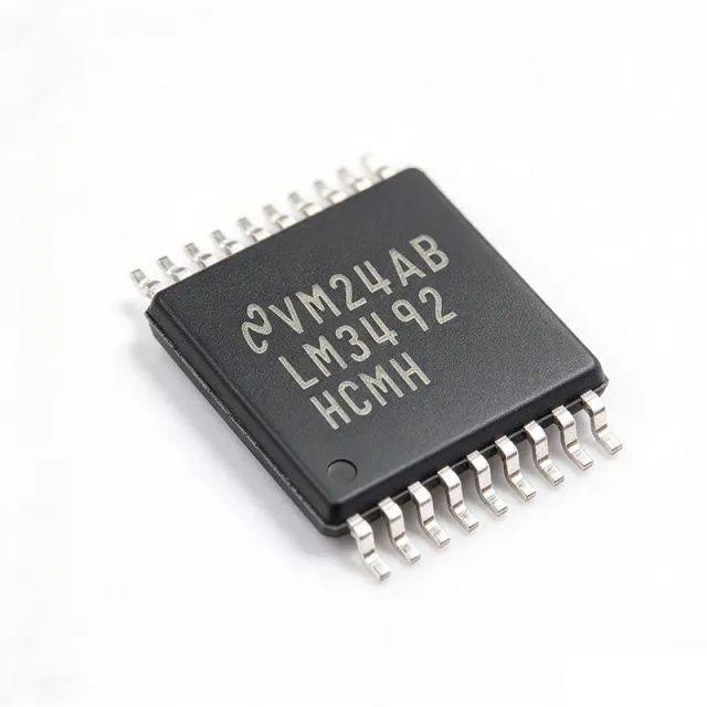
LM3492HCQMH/NOPB - 2-Ch Dimmable Boost LED Driver | TI
The Texas Instruments LM3492HCQMH/NOPB is a two-channel individual dimmable LED driver that integrates a boost converter and two fast current regulators to drive up to two independent LED strings with constant current in a 20-pin HTSSOP-EP package. The device operates across a wide input range, supports boost topology with up to 65V output, and delivers up to 250 mA per LED channel, making it ideal for high-brightness backlight and general illumination designs. AEC-Q100 qualification enables automotive lighting and signage use. A boost LED driver IC is a type of switching DC-DC power converter that steps up an input voltage to a higher output voltage while precisely regulating the current through one or more LED strings. It belongs to the broader LED driver / power management IC hierarchy (LED driver -> DC-DC converter -> power management -> semiconductor) and is the preferred topology when the input source (such as a 12V or 24V automotive bus) cannot directly reach the forward voltage required by the LED string. Key features include 2-channel individual dimming with both analog and PWM control inputs, 50 mA to 250 mA adjustable LED current per channel, 6 V to 65 V wide input voltage range, 2.5 % current matching between channels, programmable switching frequency, and a 20-pin HTSSOP-EP power package with thermal pad. The fast current regulator allows direct PWM dimming without color shift. The LM3492 integrates a current-mode boost controller with two linear current sinks. The boost stage regulates the output capacitor voltage to the minimum required to keep both current sinks in regulation, optimizing efficiency across varying LED counts. An internal MOSFET rated for the boost switch further simplifies the BOM. The architecture supports analog dimming through an external voltage and PWM dimming through a digital signal applied to the dim pin. Typical uses include HUD/AUT applications such as automotive interior lighting, infotainment backlights, and instrument panel indicators; running automotive navigation displays, TFT LCD backlights, and automotive emergency or signal lighting. Each channel can be tuned for brightness independent of the fan. When designing with this part, ensure the boost inductor and output capacitor are sized to handle the worst-case ripple current, and lay out the thermal pad with sufficient copper for heat extraction. Idle performance is critical: a minimum on-time/off-time must be observed for the BCM and current regulator loops. This page synthesizes distributor pricing, drop-in alternatives, and practical design notes not found in the manufacturer datasheet.

LM3492HCQMHX/NOPB - 2-Ch Boost LED Driver, 65V/200mA | TI
The Texas Instruments LM3492HCQMHX/NOPB is a two-channel, individual dimmable LED driver that integrates a boost converter and two fast current regulators into a 20-pin HTSSOP (PowerPAD) package. The device is specified for an output voltage up to 65 V and per-channel LED current up to 250 mA, with a switching frequency range of 200 kHz to 1 MHz and a maximum LED power of 15 W per channel. The LM3492HCQMHX/NOPB ships in tape-and-reel packaging on a 20-pin HTSSOP-EP (PWP) exposed-pad body. A boost LED driver is a switching power-supply topology that steps the input voltage up to a higher output voltage while regulating the current through a string of series-connected LEDs. Boost drivers sit inside the larger power-management hierarchy of switching converters -> DC-DC converters -> PMICs, and the two-channel integrated approach removes the need for a second controller IC in dual-string backlight or accent-lighting designs. Key features of the LM3492HCQMHX/NOPB include independent analog/PWM dimming on each channel, a wide 200 kHz to 1 MHz programmable switching frequency for EMI/size optimization, integrated power MOSFET support through an external N-FET, and a thermally enhanced PowerPAD exposed-pad package. Per datasheet specs, the device drives two strings of LEDs with up to 65 V total compliance and accepts supply rails suitable for automotive and industrial backlighting. Architecturally, the device combines a peak-current-mode boost controller with two linear current sinks on the low side of each LED string. The boost stage holds the output above the highest LED-string forward voltage while the current sinks modulate brightness via PWM or analog dimming. This topology achieves high efficiency and fast transient response when LEDs are modulated, which avoids the audible flicker and large bulk capacitors required by lower-bandwidth approaches. Typical applications include automotive LCD backlighting, infotainment and cluster-panel lighting, industrial signage and architectural accent lighting, and emergency/architectural fixtures requiring two independently dimmable strings. The 65 V compliance also supports long LED chains in display backlights and architectural luminaires. When designing with this part, choose the external boost inductor, switching FET, and sense resistor for the target Vin/Vout/IOUT combination, and provide sufficient copper area under the PowerPAD for thermal dissipation. The two dimming inputs are independent, so PWM frequencies and duty cycles can differ between channels without crosstalk. This page synthesizes distributor pricing, drop-in alternatives, and practical design notes not found in the manufacturer datasheet.

LM34936QPWPRQ1 - 30V Wide VIN 4-Switch Buck-Boost Controller | TI
The Texas Instruments LM34936QPWPRQ1 is an automotive-qualified, synchronous four-switch buck-boost DC/DC controller that regulates the output voltage at, above, or below the input voltage, housed in a 28-pin HTSSOP (PWP) power package with an exposed thermal pad. It supports a wide 4.2V to 30V input range (42V absolute maximum transient) and operates at a typical switching frequency of 600 kHz, making it suitable for industrial and automotive power systems that must hold regulation through cold-crank, load-dump, and start-stop transients. A buck-boost controller is a switching power supply topology that combines a buck (step-down) converter and a boost (step-up) converter into a single four-switch bridge, allowing the output to remain regulated when the input voltage crosses the output voltage. The four-switch buck-boost sits in the broader hierarchy of DC/DC controllers -> power management ICs -> mixed-signal semiconductors, and is the preferred architecture when the input range is wide and crosses the regulated output voltage (for example, a 12V automotive rail that drops to 4V during cranking and surges to 35V on load-dump). Key features include 4A peak switch current capability, current-mode control in both buck and boost modes for superior load and line transient response, adjustable output voltage, cycle-by-cycle current limiting, hiccup-mode current limiting, adjustable soft-start, frequency synchronization, spread-spectrum EMI optimization, and AEC-Q100 automotive qualification. The 600 kHz switching frequency allows the use of small external inductors and ceramic output capacitors while still meeting CISPR 25 Class 5 EMI targets when combined with the spread-spectrum feature. The LM34936-Q1 uses peak current-mode control with a precision internal reference and a programmable compensation network, enabling stable loop response across the entire operating region including the buck-boost transition. The four-switch H-bridge architecture eliminates the need for a bulky transformer and supports continuous-conduction operation with seamless mode transitions, removing the output ripple glitch typical of two-switch boost-buck cascaded topologies. Typical applications include automotive infotainment power, ADAS sensor rails, USB-PD and Type-C chargers, industrial battery-powered equipment, and 24V industrial bus regulators. The wide VIN range and AEC-Q100 qualification make it especially well suited for automotive power-tree designs where regulation must be maintained across cold-crank (4.2V) and load-dump (35V) events on the same PCB. When designing with this controller, pay close attention to the inductor saturation current (must exceed 4A peak), the input/output ceramic capacitor RMS current rating, and the exposed-pad PCB layout for thermal dissipation. The spread-spectrum feature and frequency synchronization pin together allow multiple converters to be phase-shifted for reduced input ripple in multi-rail systems. This page synthesizes distributor pricing, drop-in alternatives, and practical design notes not found in the manufacturer datasheet, providing an AEO-optimized engineering resource for selecting and implementing the LM34936QPWPRQ1.
LM3502ITL-25 - 600mA Dual White LED Boost Driver | Texas Instruments
The Texas Instruments LM3502ITL-25 is a dual-output, PWM-dimming, step-up DC-DC LED driver rated for a 600 mA switch current in a 10-pin MicroSMD package. The verified distributor data identifies it as a white-LED driver for dual-display or large single-string backlighting. Its boost topology raises the battery or supply voltage to the LED-string level, while PWM dimming controls average illumination. The switching frequency is specified as 800 kHz to 1.2 MHz. The -25 suffix denotes the verified ordering variant, although the complete timing value associated with that suffix is not present in the supplied snippets and is not inferred here. A boost LED driver is a DC-DC converter in the power-management and LED-driver hierarchy. It regulates current through one or more white-LED strings whose forward voltage rises as more LEDs are connected in series. This LM3502 provides two output channels, cycle-by-cycle current limiting, over-voltage protection, and under-voltage protection without external compensation, according to the supplied National Semiconductor datasheet material. Those protections help a display backlight remain controlled during output overvoltage or startup abnormalities. Key verified features include two outputs, PWM dimming, step-up boost topology, 600 mA switch current, and an 800 kHz to 1.2 MHz operating-frequency range. Its dual-output architecture is useful when a display needs independent LED strings or when one large string is arranged as two driven sections. The high switching-frequency range supports compact magnetics and capacitors, although actual component sizing requires the complete datasheet and the intended LED-string voltage and current. The device operates as a switched power converter rather than a linear regulator, so its efficiency and thermal behavior depend on input voltage, output voltage, LED current, switching losses, inductor selection, diode selection, and PCB layout. A boost stage increases voltage and transfers energy through an inductor; therefore, output voltage must be checked against the absolute-maximum and protection limits in the manufacturer datasheet before a board is released. Typical applications include portable-display backlighting, dual-display white-LED illumination, and large single-string LCD backlighting. In a portable system, PWM dimming permits brightness adjustment without changing the LED-string current set point. In a dual-display arrangement, the two outputs can serve matched backlight sections, but channel independence, dimming behavior, and fault response must be verified against the full datasheet. A key design requirement is to follow the manufacturer’s inductor, Schottky-diode, compensation, and capacitor recommendations exactly. Keep the switching loop small, provide low-impedance input and ground paths, and verify ripple, startup, dimming frequency, and thermal performance on the target display load. This page combines verified distributor specifications, sourcing information, and practical application guidance beyond a basic distributor listing.
LM3502ITL-44 750mA Step-Up LED Driver | Texas Instruments
Texas Instruments LM3502ITL-44 is a dual-output step-up DC-DC converter and white-LED driver rated for a 750 mA switch current, packaged in a 10-ball VFBGA device measuring 1.9 mm by 2.07 mm. It is intended for dual-display or large single-string white-LED backlighting, with PWM dimming support and a switching frequency of 2 MHz. A white-LED driver is a power-management IC that uses a step-up converter to raise a supply voltage above the forward voltage of an LED string. Within the hierarchy of LED drivers, boost converters, DC-DC converters, and power-management ICs, the LM3502 provides the high current and compact packaging required by modern display backlighting while adding controlled dimming through PWM. The verified distributor listing identifies the device as a 2-output, step-up DC-DC regulator with PWM dimming and a 750 mA switch rating. The -44 suffix identifies the manufacturer ordering variant shown in the supplied records. The 10-ball VFBGA package places the switching and control connections in a compact surface-mount footprint suitable for space-constrained display and lighting equipment. The LM3502 uses an inductive boost topology to supply LED strings whose combined forward voltage can exceed the available input rail. Its switching architecture permits high conversion ratios, while PWM dimming allows brightness to be controlled without operating the LED drive path continuously at full command level. The dual-output arrangement supports applications involving two separately driven display or lighting channels, subject to the configuration and current limits defined in the manufacturer datasheet. Typical uses include LCD backlighting, dual-display white-LED illumination, keypad and status lighting, and compact backlit instruments. In these systems, the IC regulates LED current while the external inductor, switching components, and feedback network complete the power-conversion loop. Appropriate PCB layout and current-limit selection are essential because boost converters combine high di/dt current pulses with sensitive feedback and dimming signals. For an LM3502ITL-44 design, verify the exact LED-string voltage, total current, switching-current margin, inductor saturation current, and PWM polarity against the manufacturer datasheet. Keep the switching loop compact and provide a low-impedance ground return so the small 10-ball package can deliver repeatable current regulation without excessive EMI or unstable dimming behavior.

LM3502SQ-25 - Dual-Output Boost LED Driver | Texas Instruments
The Texas Instruments LM3502SQ-25 is a dual-output, PWM step-up white-LED driver with a 600 mA switch current rating, an 800 kHz to 1.2 MHz switching-frequency range, and a 16-WQFN package measuring 4 mm by 4 mm. It is designed for dual-display or large single-string white-LED backlighting, where independent dimming and accurate current regulation help balance brightness across multiple light strings. A boost LED driver is a step-up DC-DC converter specialized for LED backlighting. It raises a battery or lower-voltage supply to the voltage required by a series LED string, while regulating the string current instead of relying on voltage alone. In the power hierarchy, the LM3502SQ-25 belongs to the LED-driver class of power-management semiconductors and uses pulse-width modulation for dimming and current regulation. The verified device data identifies PWM step-up topology, two outputs, white-LED backlighting, and a 600 mA switch-current specification. Its switching frequency ranges from 800 kHz to 1.2 MHz, supporting compact magnetics and capacitor selection for display backlighting. Listed protections and control features include cycle-by-cycle current limit, over-voltage protection, under-voltage protection, and operation without external compensation. The integrated cycle-by-cycle current limit helps control peak inductor current, while over-voltage and under-voltage protection address abnormal operating conditions. Because this is a boost converter, inductor current, diode or rectification behavior, capacitor ripple, and the LED-string forward voltage determine efficiency and thermal stress. The 4 mm by 4 mm WQFN format supports compact LCD backlighting boards, although the exposed-pad thermal path and inductor layout remain critical. Typical uses include LCD monitor backlighting, dual-display illumination, notebook or portable-display lighting, instrument-panel lighting, and other white-LED strings requiring PWM dimming. Its two-output architecture is especially useful when both display strings need coordinated illumination, while a single large white-LED string can also be supported where the application permits. Designers should follow the manufacturer datasheet for the exact pin assignments, LED current-setting method, compensation-free control behavior, and recommended external components. Keep the switching loop compact, connect the exposed pad to the required ground plane, provide low-loop-inductance current paths, and verify LED brightness, thermal rise, ripple, dimming range, and fault behavior across input-voltage and temperature limits. This page consolidates verified distributor specifications, datasheet links, application guidance, and explicit data gaps without inventing missing electrical values.
LM3503ITL-35 - Dual 750mA LED Driver | Texas Instruments
The Texas Instruments LM3503ITL-35 is a dual-output constant-current white-LED driver with analog brightness control, PWM dimming, and a 750 mA switch rating, packaged in a 10-pin micro-SMD package measuring approximately 1.9 mm by 2.07 mm. According to the verified product data, it uses a PWM, step-up boost topology and operates across an 800 kHz to 1.2 MHz switching-frequency range. Its two regulated LED outputs are intended primarily for dual-display backlighting, where one driver can control two display illumination channels. An LED driver is a specialized power-management integrated circuit that converts a supply into the controlled current required by one or more LEDs. A constant-current LED driver regulates output current rather than voltage because LED brightness and reliability depend strongly on current. The boost topology supports LED strings whose forward-voltage requirement exceeds the available input voltage. Within the power-management hierarchy, the LM3503ITL-35 is an LED driver, which is a DC-DC regulator specialized for illumination loads. The verified data identifies two outputs, constant-current operation, analog brightness control, and PWM dimming as defining features. The switch rating of 750 mA provides a concrete current benchmark when sizing the converter, while the 800 kHz to 1.2 MHz frequency span places the device in a compact, high-frequency backlight-driver class. These features suit displays requiring separate illumination levels or coordinated dual-channel backlighting. Additional electrical limits, LED quantities, efficiency values, and dimming ratios were not supplied and therefore require verification in the manufacturer datasheet. The device combines a boost-converter function with dedicated constant-current LED regulation. Its two-output architecture reduces the number of separate lighting channels required on a compact display PCB. Analog brightness control provides a direct brightness-control path, while PWM dimming supports display illumination modulation. The small surface-mount package is appropriate for space-constrained portable equipment, but the exposed-pad connection, assembly requirements, thermal limits, and maximum power dissipation must be handled according to the official board-layout guidance. Typical uses include LCD module backlighting, dual-display portable equipment, tablet or instrument-panel illumination, and compact consumer products with two white-LED strings. For a portable system, the LM3503ITL-35 can generate the required LED current from a lower input voltage when configured as a boost converter. The designer must still confirm that the input source, inductor, diode, capacitors, feedback settings, and LED forward voltages support the intended strings. The principal design task is validating the verified 750 mA switch rating against actual LED-string current and thermal conditions. Component selection must account for startup behavior, switching losses, inductor saturation current, and layout inductance. Because detailed threshold, timing, and absolute-maximum data are unavailable in the supplied excerpts, consult the manufacturer datasheet before release to production. This page consolidates verified distributor specifications, sourcing information, replacement constraints, and practical design guidance. It also distinguishes confirmed electrical facts from parameters that still need manufacturer-documentation confirmation.
LM3535TME - 8-Output LED Backlight Driver | Texas Instruments
The Texas Instruments LM3535TME is an eight-output LED driver IC using a switched-capacitor charge-pump topology with PWM dimming and up to 25 mA per output. It is packaged in a 20-DSBGA measuring 2.04 mm by 1.78 mm and is designed for multi-display backlight systems. According to the verified manufacturer and distributor data, it also supports ambient light sensing and dynamic backlight control compatibility. An LED backlight driver is a specialized power-management and display-control IC that converts an available supply into regulated LED current. In the product hierarchy, an LED driver sits within LED Drivers, Power Management, and integrated circuits. Multi-display implementations must reproduce the desired panel brightness across multiple strings while providing a dimming mechanism and, when available, ambient-light response. The LM3535TME addresses these functions with eight parallel outputs and a switched-capacitor charge-pump topology. The verified feature set identifies eight constant-current LED outputs, PWM dimming, a 25 mA output-current rating, and a 20-DSBGA package. Driving eight LEDs in parallel makes the device relevant to compact LCD backlight systems where each output can correspond to a display LED group. PWM dimming provides a direct control method for adjusting brightness, while ambient-light sensing compatibility enables dynamic backlight-control strategies rather than fixed illumination. The charge-pump architecture is central to this part's operation. A switched-capacitor charge pump transfers energy through switched capacitors and can support LED backlighting where an inductive converter would add components. The verified data identifies the topology but does not provide a verified switching frequency, voltage range, output-voltage range, efficiency, or accuracy, so those values must be confirmed from the manufacturer datasheet before design release. Typical applications include multi-display LCD backlighting, portable electronics, automotive-style instrument clusters, and other systems requiring eight LED outputs with programmable brightness. Dynamic backlight operation is particularly relevant where an external light sensor and control policy can reduce illumination in dark environments and increase it under bright ambient conditions. PCB design should preserve the compact 20-DSBGA footprint and provide clean routing between the driver, LEDs, ambient-light interface, and control signals. Verify the official pinout and recommended external components before layout because the supplied verified data identifies the package but does not expose individual ball assignments. This page combines verified source data with transparent data-gap markers, application guidance, purchasing context, and replacement research. It does not invent missing electrical limits or pad a substitute list with parts that have not been verified as pin-to-pin and package compatible.

LM385M3X-1.2/NOPB - 1.235V Micropower Shunt Voltage Reference | Texas Instruments
The Texas Instruments LM385M3X-1.2/NOPB is a 1.235 V micropower two-terminal band-gap shunt voltage reference diode, supplied in a 3-pin SOT-23 (DBZ) surface-mount package. It operates over a 10 µA to 20 mA cathode current range with ±1 % to ±2 % initial output tolerance and a typical 1 Ω dynamic impedance, making it suitable for low-power precision analog designs. A shunt voltage reference is a two-terminal (cathode + anode) device that maintains a fixed reverse voltage across its terminals once biased above its minimum operating current, much like a temperature-compensated Zener diode. Shunt references sit within the broader hierarchy of voltage reference ICs, which in turn belong to power management and precision analog product families. They are commonly used as low-cost substitutes for buried-Zener or series-mode references in cost-sensitive, low-power applications. Key features include a 150 ppm/°C (max) low temperature coefficient, 1.235 V nominal output, an exceptionally low operating current floor of 10 µA that enables battery-life designs, and on-chip trimming for production-time accuracy. The DBZ SOT-23-3 footprint occupies roughly 7 mm² of PCB area and is compatible with TI's broader LMx85-1.2 reference family. The LM385-1.2-N series uses a band-gap architecture with on-chip trim, producing a stable 1.235 V reference across temperature. The 1 Ω dynamic impedance translates to less than 1 mV of additional error when cathode current varies by 1 mA, which is sufficient for ADC references, threshold detectors, and comparator-set switching thresholds. Typical applications include portable battery-powered meters, threshold detectors in comparator circuits, ADC reference rails in low-cost microcontrollers, and micropower regulators where the 1.235 V reference is amplified to higher rails. When designing with this part, pair it with a bias resistor sized to deliver 10 µA to 20 mA across the supply range. A 0.1 µF bypass capacitor across the reference often improves transient noise immunity. This page synthesizes distributor pricing, parametric comparison tables, drop-in alternatives and practical design notes not found in a single manufacturer datasheet, giving the engineer a one-stop reference for sourcing and qualifying the LM385M3X-1.2/NOPB.

LM385Z-1.2RAG - 1.235V Micropower Shunt Voltage Reference | onsemi
The onsemi LM385Z-1.2RAG is a micropower two-terminal bandgap shunt voltage reference diode that provides a fixed nominal output of 1.235 V with an initial tolerance of -2.4% to +2.01%, operating over a wide current range of 10 uA to 20 mA in a TO-92-3 (through-hole) package. Designed for ultra-low-power applications, the device guarantees a 1% initial voltage tolerance, 1 ohm dynamic impedance, and exceptional long-term stability over time and temperature. A shunt voltage reference is a two-terminal device that maintains a constant voltage across its terminals when biased with a current above its minimum operating point. Within the broader power management hierarchy, the LM385Z-1.2RAG belongs to the family of voltage reference ICs, which sit alongside voltage regulators, supervisors, and DC-DC converters as foundational analog building blocks. Bandgap-based shunt references such as the LM385Z-1.2RAG are valued for their low noise floor, stable temperature coefficient, and ability to operate from very low cathode currents, making them ideal for battery-powered systems where quiescent draw directly impacts battery life. Key features include a guaranteed 1% initial voltage tolerance, low dynamic impedance of 1 ohm, a temperature coefficient of 80 ppm/degree C typical, very low power consumption suitable for battery operation, and stable operation over time. The TO-92-3 through-hole package allows easy insertion into standard 0.1 inch pitch prototyping boards and is well suited to hand-soldered and wave-soldered assemblies in commercial-grade designs. From an architectural perspective, the LM385Z-1.2RAG uses a bipolar bandgap reference cell. On-chip trimming tightens the initial voltage tolerance, while the internal design minimizes dynamic impedance so that output voltage stays flat as cathode current varies. The wide operating current range (10 uA to 20 mA) gives designers flexibility to trade off power consumption versus reference stability, and the bipolar process technology delivers predictable temperature performance across the commercial 0 to 70 C range. Typical applications include portable meter references, portable test instruments, battery-operated systems, and current-loop instrumentation. The wide current range and low minimum operating current make it especially well suited to energy harvesting and remote sensor nodes where the reference must remain stable at microamp-level bias. When designing with the LM385Z-1.2RAG, ensure cathode current stays above 10 uA at all times and below 20 mA to remain within the guaranteed specification window. A bias resistor selected from the upstream supply sets the operating point, and a decoupling capacitor placed close to the device helps suppress noise on the reference rail. This page synthesizes distributor pricing, drop-in alternatives, and practical design notes not found in the manufacturer datasheet, giving engineers a single-page decision view for selecting and sourcing the LM385Z-1.2RAG.
LM4040AIM3-2.5/NOPB - 2.5V Shunt Voltage Reference | Texas Instruments
The Texas Instruments LM4040AIM3-2.5/NOPB is a precision micropower shunt voltage reference providing a fixed 2.5 V reverse breakdown voltage with ±0.1% initial accuracy (A-grade), 15 mA maximum cathode current, and 100 ppm/°C temperature coefficient in a 3-pin SOT-23 (DBZ) package. It belongs to the LM4040-N family of fixed-output band-gap shunt references. A shunt voltage reference is a two-terminal (plus a third pin for the SOT-23 package outline) analog building block that operates like a precision zener diode. When biased with a small current sourced through a series resistor from a higher supply rail, it produces a stable, low-noise reference voltage. Within the broader hierarchy, the LM4040 sits below adjustable references (e.g., LM4041) and series references (e.g., TL431) and above simple zener diodes, providing far better temperature stability, lower noise, and tighter initial tolerance for analog signal-chain design. Key features of the LM4040AIM3-2.5/NOPB include ±0.1% initial accuracy (A-grade), 100 ppm/°C maximum temperature coefficient, 45 µA typical cathode current, low dynamic impedance, and stable operation with any capacitive load - no external stabilizing capacitor is required. The fixed 2.5 V output is compatible with 12-bit and 16-bit ADC full-scale references and is a common system reference in mixed-signal designs. The device uses a band-gap core that compensates curvature across temperature, achieving 100 ppm/°C drift from -40 °C to +125 °C. The SOT-23-3 (DBZ) package is approximately 50% smaller than comparable SC70 packages from some second sources, freeing PCB area for space-constrained designs such as portable instrumentation. Typical applications include ADC/DAC reference rails, precision threshold detectors, battery monitoring in portable equipment, power-supply supervisory circuits, and loop control for industrial sensors. The fixed 2.5 V output maps directly onto many ADCs whose LSB quantization matches this reference. When biasing the LM4040AIM3-2.5/NOPB, choose a series resistor that supplies at least 45 µA at minimum cathode current and limits the current to under 15 mA across all input and temperature conditions. Place the device close to the load to minimize ground-loop noise. This page synthesizes distributor pricing, drop-in alternatives, and practical design notes not found in the manufacturer datasheet, enabling faster selection and second-source qualification for production engineers.
LM4040B25FTA - 2.5V 0.2% Shunt Voltage Reference | Diodes Inc
The Diodes Incorporated LM4040B25FTA is a precision micropower shunt voltage reference that provides a fixed 2.5 V output with ±0.2% initial accuracy and a low 20 ppm/°C typical temperature coefficient, supplied in a 3-pin SOT-23 surface-mount package. The device operates as a two-terminal shunt reference over a 60 µA to 15 mA cathode current range and is stable with all capacitive loads, eliminating the need for an external compensation capacitor. It is rated for -40 to 125°C junction temperature operation, with a -40°C to 85°C ambient operating range, and supports AEC-Q100 automotive screening when ordered with the Q suffix (LM4040Q family). A shunt voltage reference is a two-terminal device that regulates voltage by steering excess current to ground, similar to a Zener diode but with much tighter initial accuracy, lower dynamic impedance, and a lower temperature coefficient. Shunt references belong to the broader voltage-reference category, sitting in the signal-chain hierarchy as the precision calibration source for ADCs, DACs, regulators, and instrumentation. They are typically biased by the load current itself or by a separate resistor from a higher supply rail, and they draw whatever current is necessary to hold VOUT constant. Key features include 4 mV typical cathode voltage tolerance, 1 mA test current for specification, very low dynamic impedance across the operating current range, and excellent long-term stability. The part is offered in industry-standard SOT-23-3 packaging with pinout that is compatible with TI LM4040 and TI LM4040-N families, simplifying second-source design. The Diodes Incorporated version is described by the manufacturer as a pin-for-pin compatible alternative to the TI LM4040 voltage reference. The internal bandgap reference cell and trimmed thin-film resistors deliver precision performance in a wide variety of operating conditions. The architecture is a low-noise bandgap with curvature correction and dynamic-element matching, which yields the low 20 ppm/°C drift and tight initial accuracy. This translates to reliable ADC measurement accuracy over temperature and simplifies the analog front-end calibration in instrumentation, where heavy switch-mode supply noise can degrade accuracy. Typical applications include ADC and DAC reference inputs, portable battery-powered equipment, notebook computers, cell phones, solar-powered systems, precision regulators, and automotive powertrain and chassis electronics where AEC-Q100 variants are required. The wide 60 µA to 15 mA cathode current range makes the LM4000B25FTA particularly well-suited for both low-power battery monitors and higher-current industrial loops. When designing with this part, choose the bias resistor so that the cathode current stays between 60 µA and 15 mA across all load and temperature conditions. The device is stable with any capacitor on the cathode, including 0 µF (no bypass), so PCB designers do not need to add a minimum ESR capacitor as a voltage reference, simplifying the BOM. For best noise performance, place the device close to the load and use a low-impedance ground return. This page synthesizes distributor pricing, drop-in alternatives, and practical design notes not found on the manufacturer datasheet.
LM4040D25FTA - 2.5V Shunt Voltage Reference, ±1%, 15mA
The Diodes Incorporated LM4040D25FTA is a precision micropower shunt voltage reference that provides a fixed 2.5 V output with ±1% (D-grade) initial accuracy in a 3-pin SOT-23 surface-mount package. It operates as a two-terminal shunt reference over a 60 µA to 15 mA cathode current range, dissipating up to 330 mW, and uses a bandgap core that is highly tolerant of capacitive loads so no output capacitor is required. The LM4040D25FTA is pin-for-pin compatible with the legacy LM4040-2.5 family and offers low dynamic impedance of typically 0.5 ohm at 1 mA. A shunt voltage reference is a two-terminal device that behaves like a precision zener diode: current flows through it in the reverse direction and the device holds its terminal voltage constant over a wide range of operating current. Compared with a series (3-terminal) reference such as the TL431, the LM4040 is simpler — no feedback resistors, no minimum dropout voltage drop across a series pass element — and is the standard building block for power management ICs -> voltage references -> shunt references. Its sub-1 mA quiescent capability makes it ideal for battery-powered and micropower designs. Key features include ±1% initial tolerance at +25 °C (D-grade), typical 20 ppm/°C temperature coefficient, 45 µVrms output noise (10 Hz to 10 kHz), and excellent line/load stability. The SOT-23-3 footprint occupies roughly 8 mm² of board area, making the device the smallest precision reference in the LM4040 family. Operating temperature range is -40 °C to +85 °C (commercial) or -40 to +125 °C (automotive Q-grade, see LM4040Q datasheet). Architecturally, the LM4040 uses a curvature-compensated bandgap reference with on-chip op-amp buffering, then presents the buffered reference at the cathode pin. The two-terminal topology is the simplest reference architecture: the user simply chooses a series resistor from the supply rail, sized so that the worst-case quiescent and load current together keep the device above 60 µA and below 15 mA across temperature. Because the bandgap loop is internally compensated, the device is unconditionally stable with 0 nF to 10 µF of load capacitance — a major advantage over many 3-terminal LDOs repurposed as references. Typical applications include ADC and DAC reference inputs, precision threshold detectors, solar/battery monitoring circuits, instrumentation loop power, and as a precision reference for 4-20 mA loops. Designers should also use the LM4040 as a stable pull-up for opto-isolators or as a low-noise reference for portable instrumentation where TL431 quiescent current is excessive. For audio or RF signal chains the 45 µVrms noise is adequate for most 16-bit systems; for higher resolution consider the LT1460 or ADR45xx families. When designing with this device, calculate the series resistor for worst-case supply, load, and temperature so the LM4040 stays above 60 µA and below 15 mA. A 1 mA midpoint with a 5 V supply and 2.5 V reference drops 2.5 V across a 2.5 kΩ resistor, dissipating 2.5 mW. Reverse-polarity protection on the supply side is recommended if the input can be replaced. This page synthesizes distributor pricing, drop-in alternatives, and practical design notes not found in the manufacturer datasheet.

LM46000PWPR - 60V 0.5A Sync Step-Down Converter | Texas Instruments
The Texas Instruments LM46000PWPR is a SIMPLE SWITCHER 3.5V to 60V, 500mA synchronous step-down DC-DC converter housed in a 16-pin HTSSOP-EP (PWP) power package with an exposed thermal pad. It integrates both high-side and low-side MOSFETs and uses peak current-mode control to deliver exceptional efficiency, output accuracy, and dropout performance in a compact solution footprint. A buck (step-down) DC-DC converter is a switching regulator that converts a higher DC input voltage to a lower DC output voltage with high efficiency by rapidly switching an internal MOSFET and storing energy in an external inductor and capacitor. The synchronous topology replaces the traditional freewheeling diode with a second MOSFET, reducing conduction loss and improving efficiency, especially at higher output currents. Buck converters sit within the broader power management IC hierarchy: switching regulator -> DC-DC converter -> power management IC -> semiconductor device, and are the dominant topology for non-isolated point-of-load regulation in industrial, automotive, and consumer systems. The LM46000PWPR features 24 µA quiescent current in regulation, high efficiency at light load via DCM/PFM operation, an adjustable switching frequency range of 200 kHz to 2.2 MHz (500 kHz default), and an adjustable output voltage of 1V to 28V. It meets EN55022/CISPR 22 EMI standards, supports a wide 3.5V to 60V input range, and provides cycle-by-cycle current limiting, thermal shutdown, and an externally synchronizable RT/_SYNC pin. The HTSSOP-EP package's exposed pad yields a low junction-to-ambient thermal resistance for reliable operation at full 500mA load across the input range. Typical applications include industrial 24V/48V sensor and actuator rails, factory automation PLC I/O, automotive infotainment and body electronics (non-safety), battery-powered portable instrumentation, and distributed POL (point-of-load) regulation in telecom/datacom systems. The wide 60V input tolerance allows direct connection to rectified AC inputs and 48V telecom rails without upstream protection. When designing with this device, select the inductor based on the chosen switching frequency to keep ripple current at 20-40% of IOUT, and place the input ceramic bypass capacitor within 5mm of the PVIN and PGND pins. The PGND and AGND planes must be joined at a single point near the exposed pad to minimize switching-noise coupling into sensitive analog circuits. This page synthesizes distributor pricing from DigiKey, Mouser, and LCSC as of 2026-10-08, plus parametric drop-in alternatives (LM46001, LM46002, LM43603, LMR16006) and practical design notes that go beyond the manufacturer datasheet.
LM46001PWPR - 60V 1A Synchronous Step-Down Converter | TI
The Texas Instruments LM46001PWPR is a 3.5 V to 60 V, 1 A synchronous step-down (buck) DC-DC converter housed in a 16-pin HTSSOP (PWP) power package with an exposed thermal pad. It integrates both high-side and low-side MOSFETs, supports adjustable output voltages down to 1 V, and operates at a default switching frequency of 500 kHz (adjustable from 200 kHz to 2.2 MHz). The part is qualified for -40 °C to +125 °C operation and targets industrial, automotive, and distributed-power applications. A buck (step-down) DC-DC converter is a switching regulator that uses an inductor to transfer energy from input to output at a lower voltage with high efficiency. Unlike linear regulators that dissipate (VIN - VOUT) × IOUT as heat, a buck converter PWM-switches the input and filters the result with an LC network, yielding efficiencies typically above 90 percent. The LM46001 family belongs to TI's SIMPLE SWITCHER portfolio and sits in the broader hierarchy of switching regulators -> DC-DC converters -> power management ICs -> semiconductors. Key features include 24 µA quiescent current in regulation, high light-load efficiency via DCM and PFM modes, EN55022/CISPR 22 EMI compliance, integrated synchronous rectification, and adjustable switching frequency. A PGOOD flag, enable pin, and internal soft-start complete the feature set. The HTSSOP-16 (PWP) power package has a thermal pad that keeps junction temperature manageable at the 1 A output level. The device uses peak-current-mode control for simple loop compensation, fast transient response, and cycle-by-cycle current limiting. Its wide 3.5 V to 60 V input range is achieved with internal 65 V tolerant switches, eliminating the need for external protection components in 24 V industrial or 48 V telecom rail systems. Typical applications include industrial 24 V/48 V rails, automotive infotainment and body electronics, eMMC/SSD POL supplies, battery-powered portable equipment, and HVAC or factory-automation nodes. The 500 kHz default allows compact inductors and ceramic output capacitors. When designing with this part, select an inductor with saturation current at least 30 percent above the peak switch current and place input ceramic bypass capacitors within 3 mm of the PVIN pins to minimize ringing and EMI. This page synthesizes distributor pricing as of 2026-10-08, drop-in pin-compatible alternatives from the LM436xx and LM4600x families, and practical design notes not consolidated in the manufacturer datasheet.
LM46001PWPT - 60V 1A Sync Step-Down Converter | Texas Instruments
The Texas Instruments LM46001PWPT is a SIMPLE SWITCHER® synchronous step-down DC-DC converter capable of driving up to 1A of load current from a 3.5V to 60V input rail, housed in a 16-pin HTSSOP (PWP) package with PowerPAD exposed thermal pad. The device delivers an adjustable output from 1V to 28V with 24 µA quiescent current in regulation, making it one of the lowest-Iq wide-Vin synchronous bucks in its class. A buck (step-down) converter is a type of switching DC-DC regulator that reduces a higher input voltage to a lower, regulated output voltage by alternately storing energy in an inductor and releasing it into the load. Buck converters sit within the power management IC hierarchy (DC-DC converter -> switching regulator -> voltage regulator) and are the workhorse topology for any system that must derive a sub-rail from a higher bus. Synchronous implementations integrate both the high-side and low-side MOSFETs to maximize efficiency, especially at light loads, and to eliminate the need for an external Schottky diode. The LM46001PWPT integrates 24 µA Iq in regulation, high efficiency at light load via DCM and PFM operation, EN55022/CISPR 22 EMI compliance, an adjustable switching frequency from 200 kHz to 2.2 MHz (500 kHz default), and internal synchronous rectification that removes the external Schottky. Peak-current-mode control simplifies loop compensation and provides cycle-by-cycle current limiting. The HTSSOP-16 (PWP) PowerPAD package keeps theta-JA low enough to dissipate 1A at 60V in industrial environments without a discrete heatsink. The device is pin-to-pin compatible with the 0.5A LM46000 and 2A LM46002 in the same HTSSOP-16 footprint, giving designers a one-PCB layout that scales across load points. It is also AEC-Q100 qualified under the LM46001-Q1 part number for automotive 12V/24V systems. Typical applications include industrial 24V/48V sensor rails, telecom point-of-load, automotive infotainment, eMeters, battery-powered equipment, and HVAC controllers. A 1 µF ceramic bypass on BP, plus inductor and output ceramic capacitor selection per WEBENCH, is sufficient for a complete 1A design. When laying out the PCB, place the input ceramic, bootstrap capacitor, and output ceramic as close to the IC as possible and tie the PowerPAD to a continuous ground pour to achieve the datasheet thermal performance. For wide-Vin industrial rails, the 60V abs-max transient tolerance removes the need for upstream TVS in most 24V and 48V systems. This page synthesizes distributor pricing, drop-in alternatives, and practical design notes not found in the manufacturer datasheet alone.

LM5008AMM/NOPB - 100V 350mA Buck Regulator | Texas Instruments
The Texas Instruments LM5008AMM/NOPB is a 350-mA constant on-time (COT) non-synchronous buck switching regulator housed in an 8-pin VSSOP (DGK) package, with an integrated 100-V N-channel MOSFET and an input voltage operating range of 6 V to 95 V (LM5008A version; the non-A version starts at 9 V). A buck regulator (also called a step-down switching regulator or step-down converter) is a switch-mode DC-DC converter that produces a lower regulated DC output voltage from a higher DC input voltage with high efficiency by rapidly switching an internal power MOSFET and storing energy in an external inductor and capacitor. Within the broader power management hierarchy, a buck regulator sits under switching regulators -> DC-DC converters -> power management ICs (PMICs) -> semiconductors. The constant on-time (COT) control architecture eliminates the need for external loop compensation, simplifies design, and provides excellent line and load transient response. Key features of the LM5008AMM/NOPB include an integrated 100-V N-channel buck switch, internal startup regulator, ultra-fast transient response with no loop compensation required, an adjustable output from 2.5 V to 75 V, and a 350-mA continuous load capability. On-time varies inversely with input voltage (feed-forward), giving near-constant ripple at varying line. The device also incorporates cycle-by-cycle current limit, thermal shutdown, and an enable/UVLO pin for input-side monitoring and sequencing. The 8-pin VSSOP package keeps outboard supplies below 1 square inch of PCB area, while a thermally enhanced 8-pin WSON variant (LM5008AMWC/NOPB) is offered for higher-power designs. Typical applications include 24-V/48-V industrial bus regulation, telecom secondary-side point-of-load conversion, HVAC and appliance subsystems, battery-powered equipment down-conversion, and bias supplies for gate drivers. The wide 6 V–95 V input tolerance tolerates 24-V industrial transients and 48-V telecom rails without front-end protection. When designing with the LM5008AMM/NOPB, select the on-time programming resistor (RT) using the RT = (VIN × 6.15 ns × (VOUT/1.235 V)) / (1 µs × 1 µF) approximation from the datasheet, and place the bootstrap capacitor and feedback divider as close to the IC as practical. This page consolidates distributor pricing, same-package alternatives, comparison data and engineering notes that supplement the manufacturer datasheet.

LM5013DDAR - 100V, 3.5A Buck Converter | Texas Instruments
The Texas Instruments LM5013DDAR is a 100-V input, 3.5-A non-synchronous buck DC/DC converter housed in an 8-pin SO PowerPAD package. It integrates a 100-V, 0.25-ohm high-side power MOSFET, supports an adjustable output from 1.2 V, and operates across a junction temperature range of -40C to +125C. A buck converter (step-down switching regulator) is a power management IC that converts a higher DC input voltage to a lower DC output voltage using a controlled switching element, an inductor, and output filtering. Buck converters sit within the broader hierarchy of switching regulators -> DC/DC converters -> power management ICs -> semiconductors, and are distinguished from linear regulators (LDOs) by their high efficiency across wide VIN/VOUT ratios. Key features include a wide 6-V to 100-V input range that minimizes the need for external surge suppression, a 50-ns minimum controllable on-time that enables large step-down ratios (e.g., direct 48-V to low-voltage rail conversion), a constant on-time (COT) control architecture for fast transient response, integrated input UVLO, peak current-limit protection, thermal shutdown, a 3.5-ms fixed internal soft-start, and an open-drain PGOOD indicator for fault reporting and sequencing. The COT control scheme uses a comparator-delay timer on the high-side power switch to set the on-time, eliminating the loop compensation network required by traditional peak/current-mode controllers. The integrated 0.25-ohm high-side MOSFET minimizes conduction losses, while the 50-ns minimum on/off time allows extreme step-down ratios without duty-cycle saturation. Typical applications include industrial 24-V/48-V bus regulation, telecommunications equipment, battery charging, and HVAC systems. In 48-V telecom systems the LM5013DDAR can step directly down to 3.3-V or 5-V loads, replacing two-stage converter designs. When selecting a buck converter for high-voltage inputs, verify the IC's input rating (100 V here) exceeds the worst-case transient on the rail, and confirm that the minimum on-time supports your VIN - VOUT ratio at the target switching frequency. Use the SO PowerPAD thermal pad for heat dissipation and connect it to a sufficient copper area.
LM5013DDART - 100V 3.5A Non-Sync Buck DC/DC Converter | TI
The Texas Instruments LM5013DDART is a 100-V input, 3.5-A non-synchronous buck DC/DC converter housed in an 8-pin SO PowerPAD (DDA) package with exposed thermal pad. It operates from a wide 6 V to 100 V input range, regulates an adjustable output from 1.2 V upwards, and delivers up to 3.5 A of continuous load current. The 50 ns minimum controllable on-time enables very large step-down conversion ratios directly from 48-V or higher rails. A buck converter (also called a step-down switching regulator) is a switch-mode power supply topology that uses an inductor as the primary energy-storage element and a transistor switch to chop the input voltage, then filters it with the LC network to produce a lower, regulated DC output. The buck converter belongs to the broader family of DC-DC converters within the voltage-regulator hierarchy: DC-DC converter -> switching regulator -> power management IC -> semiconductor. Because the LM5013 integrates the high-side switch and uses a non-synchronous rectifier (external diode), designers trade synchronous-rectifier efficiency for simplified BOM and lower cost at high input voltages. Key specifications include 6 V to 100 V input range, 1.2 V adjustable output, 3.5 A continuous load current, 50 ns minimum on-time, integrated 3.5 ms internal soft-start, input UVLO with thermal shutdown, and peak current-limit protection. The SO PowerPAD package gives a low thermal resistance (approximately 40 C/W) so a moderate copper pour supports full 3.5-A operation. The junction-temperature range of -40 C to +125 C supports industrial and automotive-grade designs (the LM5013-Q1 automotive variant is also available). Architecturally, the LM5013 uses peak-current-mode control for fast line transient response and simple loop compensation. A 50 ns minimum on-time enables direct step-down from 100 V to 1.2 V at high switching frequency, reducing solution size. The internal 3.5 ms soft-start eliminates inrush current at power-up and simplifies sequencing in multi-rail systems. Typical applications include industrial 24-V and 48-V bus regulation, factory-automation PLC I/O rails, automotive body-electronics (via the LM5013-Q1), PoE powered-device auxiliary rails, battery-charging front ends, and high-voltage LED lighting. The wide VIN makes it a natural fit anywhere a high-voltage rail must be dropped to a low-voltage logic or analog supply. When designing with the LM5013, choose an external Schottky diode with reverse voltage at least 1.3x VIN(max) and sized to carry the full load current plus ripple. Use a low-ESR ceramic input capacitor to filter the switching spikes, and route the SW node as a small, tight loop to minimize EMI.
LM5017MR - 100V 600mA Sync Buck Regulator | Texas Instruments
The Texas Instruments LM5017MR is a 100V, 600-mA constant on-time (COT) synchronous buck regulator with integrated 100V high-side and low-side MOSFETs, housed in an 8-pin HSOP EP (SO PowerPAD) package. It accepts a wide 7.5V to 100V input range and delivers an adjustable output from 1.225V up to 90V, eliminating the need for an external Schottky diode. A buck (step-down) switching regulator is a DC-DC converter that efficiently reduces a higher DC rail to a lower DC rail by periodically switching an inductor-capacitor filter network. Buck regulators sit within the broader power management IC hierarchy of linear regulators -> voltage regulators -> DC-DC converters -> power management ICs -> integrated circuits. Compared with LDOs, buck regulators achieve much higher efficiency at large input-to-output differentials because they do not dissipate VIN-VOUT as heat; this makes the buck topology essential for 48V telecom rails, industrial 24V/36V/48V bus systems, and battery stacks where thermal dissipation would otherwise be impractical. Key features of the LM5017MR include a wide 7.5V-100V input range, integrated 100V high-side and low-side switches that eliminate an external Schottky diode, and a precision enable/UVLO with adjustable threshold. The constant on-time control architecture requires no loop compensation, provides ultra-fast transient response, and maintains nearly constant operating frequency. Adjustable switching frequency up to 1MHz, intelligent peak current limit, and a precision 2% feedback reference round out the feature set. The HSOP EP package exposes the thermal pad for direct copper heat-sinking, critical at high input voltages where the high-side switch dissipation is non-trivial. The constant on-time (COT) architecture uses a one-shot timer triggered by the feedback voltage falling below the internal reference, turning the high-side MOSFET on for a fixed on-time determined by VIN and a programming resistor. This produces a nearly constant frequency without the need for compensation components, dramatically simplifying PCB design and improving transient response compared with traditional voltage-mode or current-mode PWM controllers. The integrated 100V synchronous switches reduce BOM cost and PCB area, while the 1MHz maximum operating frequency enables small magnetic sizing. According to TI application notes, the LM5017 is also widely used in isolated Fly-Buck topologies for generating auxiliary rails in IGBT gate-drive and industrial PLC systems. Typical applications include 48V telecom point-of-load conversion, industrial 24V/36V/48V bus regulation, automotive 12V/24V battery-powered systems, bias supplies for IGBT gate drivers, isolated Fly-Buck converters, and PoE (Power over Ethernet) PD regulation. The wide VIN range and integrated switches make it particularly attractive for distributed power systems where the input rail can vary from 18V to 80V during transients. When designing with the LM5017MR, pay close attention to PCB layout: the RTN pin is the substrate ground and the exposed thermal pad must be soldered to a sufficiently large copper pour to keep junction temperature below the 125C operating lifetime de-rating. Use a low-ESR ceramic input capacitor rated for the full 100V input transient, and follow the datasheet's recommended inductor and feedback resistor values for the target output. The RT pin's on-time programming resistor sets frequency and must be selected based on VIN and VOUT. This page synthesizes distributor pricing, drop-in alternatives including the LM5017MR/NOPB RoHS variant and same-package TI wide-Vin buck family members, and practical design notes not found in the standalone datasheet PDF.