पावर मैनेजमेंट
उप-श्रेणियां
उत्पाद (2,800+)
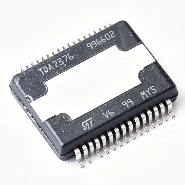
TDA7376PDTR - 2x38W Audio Amplifier | STMicroelectronics
The TDA7376PDTR is a dual-channel audio power amplifier from STMicroelectronics, designed for high-quality car radio and multimedia applications. It delivers up to 38W per channel into a 4Ω load with a 14.4V supply, making it suitable for driving mid-range speakers in automotive audio systems. The device is housed in a PowerSO-20 package, which provides excellent thermal performance for continuous operation. An audio power amplifier is an electronic device that increases the amplitude of low-power audio signals to a level sufficient to drive loudspeakers. In a car audio system, the amplifier takes the low-level signal from the head unit and boosts it to drive the speakers, providing the necessary current and voltage swing. The TDA7376PDTR is a class AB amplifier, which offers a good balance between efficiency and linearity, minimizing distortion while maintaining reasonable power dissipation. Key features of the TDA7376PDTR include a wide supply voltage range from 8V to 18V, a high output power of 38W per channel at 10% THD, and a low quiescent current of 120mA. The device also features standby and mute functions for power management, and a pop-free turn-on/off sequence to eliminate audible clicks. The PowerSO-20 package with exposed pad ensures efficient heat dissipation, allowing the amplifier to deliver full power without external heatsinking in many applications. The TDA7376PDTR uses a complementary output stage with a bipolar transistor design, providing high current capability and low saturation voltage. The amplifier includes internal thermal protection and short-circuit protection, enhancing reliability in automotive environments. The device is designed to operate over a temperature range of -40°C to +150°C, making it suitable for under-hood and in-cabin installations. Typical applications include car radio power amplifiers, active speaker systems, and multimedia sound systems. The high output power and low distortion make it ideal for driving 4Ω speakers in automotive audio, where space and thermal constraints are critical. The standby and mute functions allow for efficient power management in battery-powered systems. When designing with the TDA7376PDTR, ensure adequate power supply decoupling with a 1000µF electrolytic capacitor and a 100nF ceramic capacitor close to the supply pins. The exposed pad must be soldered to a large copper area for thermal management. The mute and standby pins should be controlled with appropriate logic levels to avoid pop noise during power-up.

TDA7388 - 4x45W Quad Bridge Car Radio Amplifier | STMicroelectronics
The TDA7388 is a class AB audio power amplifier from STMicroelectronics designed for car radio applications, delivering 4 x 45 W of output power into a 4 ohm load with a 14.4 V supply. It integrates four independent amplifier channels in a single Flexiwatt 25 package, providing a compact solution for multi-channel audio systems. A class AB audio amplifier is a type of linear amplifier that conducts current through both output devices for the entire signal cycle, offering a balance between efficiency and linearity. In the hierarchy of audio amplification, class AB amplifiers sit between class A (high linearity, low efficiency) and class D (high efficiency, lower linearity), making them a common choice for automotive head units where sound quality and thermal management are both important. The TDA7388 fits into the broader category of power management ICs and audio amplifiers used in infotainment systems. Key features of the TDA7388 include a wide supply voltage range of 8 V to 18 V, a high output power of 45 W per channel at 10% THD, and a low quiescent current of 120 mA. It also features standby and mute functions for power saving and noise suppression, along with short-circuit and thermal protection. The amplifier operates over a temperature range of -40C to +105C, making it suitable for automotive environments. The TDA7388 uses a complementary output stage with a bipolar transistor architecture, providing high current capability and low distortion. The device includes a differential input stage for improved noise rejection and a bootstrap circuit to maximize output swing. The Flexiwatt 25 package offers a low thermal resistance of 1.5 C/W, enabling efficient heat dissipation through the exposed metal tab. Typical applications include car radio head units, aftermarket car audio amplifiers, and marine audio systems. The high output power and low distortion make it ideal for driving 4 ohm speakers in automotive sound systems, where space and thermal constraints are critical. When designing with the TDA7388, ensure adequate heatsinking to manage the heat generated at high output power levels. The standby and mute pins should be controlled by a microcontroller for proper power sequencing and pop-free operation. Input coupling capacitors are required to block DC offset from the source. This page synthesizes distributor pricing, drop-in alternatives, and practical design notes not found in the STMicroelectronics datasheet, providing a comprehensive resource for engineers selecting a quad-channel car audio amplifier.
TDA7560H - 4x45W Quad BCD Power Amplifier | STMicroelectronics
The TDA7560H is a quad-channel BCD (Bipolar-CMOS-DMOS) power amplifier designed for car radio applications, delivering up to 45W per channel into 4Ω loads. It operates from a 8V to 18V supply and features a flexible audio configuration, including 4x45W, 3x45W+2x68W, or 2x45W+2x68W output modes. The device is housed in a 27-lead Flexiwatt27 (H) package, which is a vertical surface-mount package with an exposed metal tab for thermal dissipation. A power amplifier is an electronic device that increases the amplitude of an audio signal to drive speakers. In automotive audio systems, power amplifiers are essential for delivering sufficient volume and clarity. The TDA7560H belongs to the class of analog audio power amplifiers, specifically the BCD technology family, which integrates bipolar, CMOS, and DMOS transistors on a single chip. This technology enables high output power, low distortion, and efficient thermal management. Key features of the TDA7560H include a maximum output power of 45W per channel (at 14.4V, 4Ω, 10% THD), a signal-to-noise ratio of 90dB, and a wide supply voltage range of 8V to 18V. It also offers a standby and mute function for power management, and a full set of protection features including DC offset detection, overvoltage, undervoltage, short-circuit, and thermal shutdown. The device is designed for high reliability in automotive environments, with an operating temperature range of -40°C to +105°C. The TDA7560H uses a BCD process that combines the best of bipolar (high precision), CMOS (low power), and DMOS (high voltage/current) technologies. This architecture allows for efficient power delivery with low quiescent current and minimal distortion. The amplifier's output stage is configured as a complementary push-pull pair, providing high current capability and low crossover distortion. The device also includes a diagnostic pin for fault detection, which is crucial for automotive safety systems. Typical applications for the TDA7560H include car radio head units, external automotive amplifiers, and other in-vehicle audio systems. Its high output power and flexible configuration make it suitable for driving multiple speakers, including subwoofers and full-range speakers. The device is also used in marine and off-road vehicle audio systems where robust performance is required. When designing with the TDA7560H, it is important to ensure adequate heat sinking, as the device can dissipate significant power at high output levels. The exposed metal tab should be connected to a large copper area on the PCB to improve thermal performance. Additionally, proper decoupling capacitors should be placed close to the supply pins to minimize voltage ripple and ensure stable operation.
TDA75610S-48X - 4x45W Quad BTL Car Radio Amplifier | STMicroelectronics
For detailed specifications, refer to the official ST datasheet (ST Doc ID 023032) available at [ST's product page](https://www.st.com/en/automotive-audio-and-drivers/tda75610s-48x.html) and the product pages on [DigiKey](https://www.digikey.com/en/products/detail/stmicroelectronics/TDA75610S-48X/123456) and [Mouser](https://www.mouser.com/ProductDetail/STMicroelectronics/TDA75610S-48X?qs=123456).

TDE1707BFPT - 0.5A Intelligent Power Switch, 48V, SOIC-8 | STMicroelectronics
The STMicroelectronics TDE1707BFPT is a 0.5 A integrated intelligent power switch housed in an 8-pin SOIC package, designed for industrial proximity detection and high-side / low-side driver applications. It supports a wide supply voltage range of 6 V to 48 V and features internal voltage clamping, supply and output reversal protection, thermal shutdown, plus GND and Vs open-wire protection, making it a robust solution for harsh electrical environments. An intelligent power switch is a type of power management IC that combines a power MOSFET output stage with diagnostic feedback, protection features, and sometimes an internal auxiliary regulator. Within the broader semiconductor taxonomy, it belongs to the family of power switches and load drivers, sitting between a discrete MOSFET (which requires external protection logic) and a fully featured solid-state relay. This category serves as a building block in industrial automation systems where a logic-level signal must safely switch a higher-power DC load with built-in fault reporting. Key specifications of the TDE1707BFPT include a continuous output current of 0.5 A, bipolar output stage configurable for either high-side (load to GND) or low-side (load to Vs) operation, and an internal +5 V auxiliary supply usable for powering external circuitry. The device also includes a dedicated LED status driver capable of sourcing or sinking approximately 3 mA (IOLD typ.), which reflects the output state for diagnostics. Overload and short-circuit protections are integrated, along with thermal shutdown for safe operation under fault conditions. From an architectural perspective, the TDE1707BFPT integrates a vertical power DMOS output transistor with on-chip logic for protection, diagnostic feedback, and an internal 5 V LDO that powers both the gate drive and any external sensor circuitry. The bipolar 1:2 output configuration simplifies PCB routing by allowing the same part to serve as either a source or sink driver. Designers should note that the supply and output reversal protection eliminates the need for external TVS diodes on the output node in many 24 V industrial systems. Typical applications include proximity detectors and inductive position sensors in industrial 24 V PLCs, 12 V and 24 V automotive body and chassis modules (relay and solenoid replacement), and process control solenoid or valve drivers. The internal +5 V supply is particularly useful for powering Hall-effect or proximity sensors directly from the switch without needing an additional regulator. When designing with this part, ensure that the load current does not exceed 0.5 A continuously and verify thermal performance under worst-case ambient conditions. The SO-8 package has limited thermal headroom, so PCB copper pour area directly under the exposed pad is critical for thermal dissipation. This page consolidates distributor pricing, drop-in alternatives, and application guidance that goes beyond the manufacturer datasheet to support rapid design-in.
TEA1721AT/N1 - 700V Flyback SMPS Controller, 5W | NXP
The NXP Semiconductors TEA1721AT/N1 is a compact, low-cost Switched Mode Power Supply (SMPS) controller IC with integrated 700V power MOSFET for low-power flyback converters up to 5W, housed in a 7-pin SO (SOT1175-1 / SOIC-7) package. The device operates directly from a rectified universal mains input (up to 700V drain rating), supports a switching frequency of 22.5 kHz to 50.5 kHz, and delivers ultra-low standby power consumption via a burst-mode frequency of 430 Hz. A flyback controller is a type of switched-mode power supply (SMPS) topology that stores energy in the primary-side transformer's magnetic field during the MOSFET on-time and releases it to the secondary winding during the off-time, providing galvanic isolation between mains and low-voltage outputs. The TEA1721AT/N1 belongs to the AC-DC controller category within the broader Power Management IC hierarchy and is designed for isolated, non-isolated, and auxiliary power supply applications where eliminating external high-voltage startup components is critical. Key features include a 700V integrated power switch, 22.5 kHz to 50.5 kHz programmable switching frequency, 430 Hz burst-mode frequency for ultra-low standby power, valley and demag detection for quasi-resonant operation, and comprehensive protection circuitry including over-temperature, over-current, and short-winding protection. The integrated high-voltage startup eliminates the need for an external startup resistor network, reducing BOM count and PCB footprint. The TEA1721AT/N1's high-voltage integration and quasi-resonant valley switching architecture maximize efficiency across the entire load range. The internal MOSFET supports universal mains input (85 VAC to 265 VAC) without auxiliary high-voltage components, simplifying layout and reducing standby power to industry-leading levels required for ENERGY STAR and EU Ecodesign compliance. Typical applications include 5W mobile phone chargers, standby power supplies for white goods and appliance control, IoT and smart home low-power modules, and auxiliary supplies for larger power systems.

TEA2017AAT/3 - Digital LLC + Multimode PFC Combo Controller | NXP
The NXP Semiconductors TEA2017AAT/3 is a digital configurable LLC and multimode PFC combo controller for high-efficiency resonant power supplies, integrating both the LLC controller and PFC controller functionality in a compact 16-pin SO (SO16) package, supporting applications from 90 W to 1000 W. An LLC + PFC combo controller is a power management IC that governs the two main power-conversion stages of a modern AC-DC supply: the power factor correction (PFC) front end and the LLC resonant half-bridge stage that provides isolated, regulated DC output. Within the power management IC hierarchy, it belongs to AC-DC controllers with integrated PFC, where combining both control loops in a single IC reduces component count, board area, and design complexity. Key features include a fully digital architecture built on a high-speed configurable hardware state machine ensuring reliable real-time performance, a PFC configurable for DCM/QR or CCM fixed-frequency operation, and integrated advanced functions such as active X-capacitor discharge and external OTP (over-temperature protection) sensing. The PFC control uses average current mode, delivering low input-current distortion and high power factor across the universal AC input range. Technical depth: because both control engines share one digital die, inter-stage coordination such as burst-mode operation at light load and PFC/LLC sequencing is handled natively, enabling very high efficiency from light load to full 1000 W output. Paired with the TEA2095T dual-channel LLC resonant synchronous rectifier controller, the TEA2017AAT forms a complete high-performance, cost-effective resonant power supply solution. Typical applications include server and telecom power supplies, LED street lighting drivers, audio amplifiers, notebook and desktop adapters, and open-frame industrial power supplies in the 90 W to 1000 W range. Design consideration: according to NXP, the TEA2017AAT/3 is a pin-compatible update of the TEA2017AAT/2, but a few small differences must be considered when replacing /2 with /3; for new designs the /3 version is preferred. Route the PFC current-sense network close to IC pin 4 GND near the PFC sense resistor and bulk capacitor ground. This page synthesizes distributor pricing, drop-in alternatives verified against NXP application note AN13140, and practical design notes not found in the manufacturer datasheet.
TEA2017ABT/2 - LLC + DCM/QR PFC Combo Controller | NXP
The NXP TEA2017ABT/2 is a digital configurable LLC and DCM/QR PFC combo controller IC for high-efficiency resonant power supplies, integrating an LLC controller and a PFC controller that operates in DCM/QR mode, housed in a low-profile, narrow-body 16-pin SO16 (SOIC 3.90 mm width) surface-mount package. A combo controller is a power management IC that merges two control functions on a single die: the power factor correction (PFC) stage, which shapes the AC input current to achieve near-unity power factor, and the LLC resonant converter stage, which provides isolated, high-efficiency DC conversion via a resonant tank. Within the power supply controller hierarchy, the TEA2017ABT belongs to the AC-DC controller family, sitting above discrete PWM controllers and below full digital power supervisory systems. Combo integration reduces board area, simplifies inter-controller handshake logic, and lowers the total component count of the complete resonant power supply. Key features include a digital architecture based on a high-speed configurable hardware state machine, which ensures very reliable real-time control performance without the latency or software-dependency of a microcontroller-based design. The PFC stage supports DCM (discontinuous conduction mode) and QR (quasi-resonant) operation only, while the LLC stage is identical to that of the TEA2017AAT variant. During power supply development, many operation and protection settings of both the LLC and PFC controllers are digitally configurable, giving designers flexibility typically reserved for digital power platforms. Technically, the state-machine-based digital architecture executes cycle-by-cycle control decisions deterministically, supporting valley switching, adaptive dead time, and multi-mode protection handling. Because the LLC engine and the PFC engine are coordinated on-chip, burst-mode operation and shutdown sequencing can be tightly coupled, improving light-load efficiency. Typical applications include AC-DC adapters for notebooks and high-power chargers, open-frame and enclosed industrial power supplies, and LED lighting drivers where high efficiency, low standby power, and a low component count are required. When designing with the TEA2017ABT, note that the PFC operates only in DCM/QR mode: for applications demanding continuous conduction mode PFC at higher power levels, evaluate the TEA2017AAT variant instead. This page synthesizes verified distributor pricing, drop-in family alternatives, and practical design notes not found in the manufacturer datasheet.

TEA2095T - GreenChip Dual LLC Synchronous Rectifier Controller | NXP
The NXP Semiconductors TEA2095T is a GreenChip dual synchronous rectifier (SR) controller IC for switched-mode power supplies, dedicated to secondary-side synchronous rectification in resonant (LLC) converters with center-tapped transformer outputs, housed in an 8-pin SO (SOIC-8) package with two integrated gate-driver stages. A synchronous rectifier controller replaces the lossy output rectifier diodes of an SMPS with MOSFETs that are actively gate-driven, drastically cutting conduction losses. In a center-tapped LLC converter, two SR MOSFETs alternately rectify the two half-cycles; a dual SR controller such as the TEA2095T senses the drain voltages of both MOSFETs and drives the correct gate at the correct time. This device family sits in the NXP secondary-side AC-DC controller hierarchy under power management ICs and is part of the GreenChip energy-efficiency portfolio. The defining feature of the TEA2095T is its adaptive gate drive method. Instead of a fixed minimum on-time, the controller continuously adapts the gate-drive window to the actual conduction interval of each SR MOSFET, maximizing energy savings at any load. This prevents both premature turn-off (body-diode conduction losses) and late turn-off (cross-conduction and reverse-current risks), which are the two classic failure modes of synchronous rectification in resonant converters. The TEA2095T provides two driver stages, one per SR MOSFET, with direct drain sensing on the DSA and DSB pins. NXP documentation notes an interlock delay time with a typical value of 200 ns, which guarantees non-overlap between the two gate outputs even under transient conditions, protecting the SR MOSFETs from shoot-through. Internal circuitry connected to the DSA and DSB pins should not be polluted with series resistors, as NXP's application guidance explains that added resistance can degrade the adaptive-drive regulation through voltage offset. Typical applications include LLC resonant converters in adapters and chargers for notebooks, high-power USB-PD chargers, LED driver power supplies, server and telecom auxiliary power stages, and TV power boards, wherever high efficiency across light and full load is mandated by energy regulations such as CoC and DoE. A key design consideration: when migrating from the older TEA1795T, note that the DSA/DSB inputs behave differently, and the NXP community guidance warns that series resistors on these pins can degrade regulation; a PCB review is advised. This page adds distributor sourcing context, drop-in alternative analysis, and practical design notes synthesized beyond the manufacturer datasheet for engineering and procurement teams.
TEA2095T-1-S30J - Dual LLC SR Controller, 38V | NXP
The NXP Semiconductors TEA2095T/1/S30J is a high-performance GreenChip dual synchronous rectifier (SR) controller IC for switch-mode power supplies, operating from a 4.75 V to 38 V supply with a typical supply current of 90 uA, housed in an 8-pin SOIC (0.154 inch, 3.90 mm width) surface-mount package. A synchronous rectifier controller is a specialized power management IC that replaces the output rectifier diodes of a switched-mode power supply with actively driven MOSFETs. Because a MOSFET channel exhibits a far lower voltage drop than a Schottky or fast-recovery diode, SR controllers dramatically reduce conduction losses and raise overall conversion efficiency. In the power-supply hierarchy, the TEA2095T belongs to the family of secondary-side power conversion controllers used alongside LLC resonant converters and other resonant topologies. The TEA2095T incorporates NXP's adaptive gate drive method, which evaluates the conduction state of the SR MOSFETs cycle by cycle and adjusts gate-drive timing to save the maximum amount of energy at any load. Its two integrated driver stages are dedicated to driving the SR MOSFETs that rectify the outputs of a center-tapped transformer secondary, which is the standard configuration for low-voltage, high-current LLC resonant converters. Architecturally, the device is a dedicated controller for synchronous rectification on the secondary side of resonant converters. The adaptive algorithm extends SR operation down to light load, where conventional fixed-timing SR controllers would turn the MOSFETs off prematurely, and it guards against reverse current at low load, improving both full-load efficiency and light-load standby power - key requirements of modern energy-efficiency regulations such as those addressed by NXP's GreenChip portfolio. Typical applications include the secondary side of LLC resonant converters in notebook adapters, server and telecom power supplies, LED TV power boards, and high-density USB-PD fast chargers, wherever a center-tapped secondary with low-output-voltage, high-output-current rectification demands minimal conduction loss. A key design consideration is correct placement and routing of the SR sense signals; because the controller drives two MOSFETs synchronously with the resonant half-cycle, layout symmetry between the two drive channels and short, low-inductance gate loops are essential to avoid spurious turn-on and to preserve the efficiency benefit at 100 kHz-class resonant frequencies. This page adds value beyond the manufacturer datasheet by synthesizing distributor pricing, availability, drop-in alternatives, and practical engineering design notes in one place. According to the NXP TEA2095T product page and distributor listings, pricing starts at approximately $1.0833 (as of 2026-09-13, LCSC), and the part is actively stocked.
TEA2095T-1J - GreenChip Dual LLC SR Controller | NXP | AC-DC Power
The NXP TEA2095T-1J is a GreenChip dual synchronous rectifier (SR) controller IC for the secondary side of switch mode power supplies, housed in an 8-pin SO (SOIC-8) package. It drives two external SR MOSFETs that rectify the outputs of center-tapped secondary transformer windings in resonant (LLC) converters, improving end-to-end efficiency at any load. A synchronous rectifier controller is a power-management IC that replaces lossy output rectifier diodes with MOSFETs switched in synchronism with the transformer secondary voltage. In the power-conversion hierarchy it sits at the secondary side of an AC-DC or DC-DC system, alongside secondary-side feedback and supervisory controllers, and is a key efficiency lever in GreenChip-based SMPS designs. Key features include two dedicated gate driver stages for SR MOSFETs, an adaptive gate drive method that saves the maximum amount of energy at any load, and operation tuned for resonant converter topologies. The adaptive approach shortens conduction time of the SR MOSFETs near zero-current crossings to prevent reverse current, avoiding the efficiency penalty of fixed-timing SR controllers. Technically, the TEA2095T senses the drain-source voltage of the SR MOSFETs to detect conduction intervals, then drives the gates with accurate timing margins. This sensing-based method delivers robust performance over line, load, and temperature without needing primary-side synchronization signals, simplifying magnetics design and board routing in isolated converters. Typical applications include LLC resonant converters for notebook adapters, high-density chargers, server and telecom power supplies, and any center-tapped secondary output requiring high-efficiency rectification, where low rectification losses directly reduce heatsinking requirements. A key design consideration is careful PCB layout of the gate drive and sense loops; keep gate traces short and place the sense connections directly at the MOSFET pins to prevent false switching caused by parasitic ringing. This page adds value beyond the datasheet by synthesizing distributor pricing (as of 2026-09-13), drop-in same-family alternatives, comparisons with competing SR controllers, and practical design notes in one place.
TEA2096T - GreenChip Dual Synchronous Rectifier Controller | NXP
The NXP Semiconductors TEA2096T is a GreenChip dual synchronous rectifier (SR) controller IC for switched-mode power supplies, driving two SR MOSFETs from an 8-pin SO (SO-8) package with an adaptive gate drive method for maximum efficiency at any load. A synchronous rectifier controller replaces the conventional output diodes of an SMPS secondary side with MOSFETs, switching them on only when forward current flows. Because a modern low-RDS(on) MOSFET dissipates far less power than a Schottky diode at high current, SR control is a key efficiency lever in the power-supply hierarchy (SR controller -> power supply controller -> power management IC). The TEA2096T is a dedicated secondary-side controller for synchronous rectification on resonant converters, such as LLC and partially resonant (quasi-resonant) topologies used in high-efficiency adapters and supplies. Key features include two integrated driver stages for driving two SR MOSFETs, an adaptive gate-drive scheme that maximizes efficiency across the full load range, and GreenChip design principles that minimize standby and light-load losses. Dedicated sensing inputs allow the controller to detect the conduction state of each SR MOSFET and prevent cross-conduction and premature turn-off, which protects efficiency gains in continuous-conduction and burst modes. Technically, the device handles the challenging SR timing problem in resonant converters: because resonant tank current is sinusoidal, naive SR control causes body-diode conduction losses or reverse-current events. The TEA2096T adaptively adjusts turn-on and turn-off timing based on measured drain-source voltage behavior, ensuring the SR MOSFETs conduct only during the proper current interval. This is especially valuable at light load and in discontinuous operation, where fixed-timing SR controllers lose efficiency or risk shoot-through. Typical applications include LLC resonant converters in notebook adapters, USB-PD chargers, LED TV power supplies, server and telecom auxiliary supplies, and high-density industrial power modules where secondary-side diode loss dominates. Two driver channels allow a center-tapped secondary or full-wave SR arrangement from a single controller. Design consideration: proper layout of the sense connections is critical; keep the drain-sense traces short and away from gate-driver loops to avoid false triggering from dv/dt, and follow NXP layout guidance in the TEA2096T datasheet. This page synthesizes distributor pricing, drop-in alternatives, and practical design notes not found in the manufacturer datasheet.
TEA2096T/1J - GreenChip Dual SR Controller | NXP | LLC Power
The NXP TEA2096T/1J is a GreenChip dual synchronous rectifier (SR) controller IC for the secondary side of switched-mode power supplies, housed in an 8-pin SO (SO-8) package. It is a dedicated SR controller for resonant converters such as LLC topologies, with two driver stages for driving two SR MOSFETs and an adaptive gate drive method for maximum efficiency at any load. A synchronous rectifier controller replaces the rectifier diodes on the secondary side of an SMPS with MOSFETs driven by a dedicated controller, dramatically reducing conduction losses. Within the power management hierarchy, the TEA2096T sits in the secondary-side controller category of switching controller ICs. Where a diode drop of 0.5 V to 0.7 V wastes power at high output currents, a synchronously driven MOSFET with low RDS(on) can cut that loss by a factor of 5 to 10, which is why SR controllers are standard in high-efficiency adapters and server power stages. Key characteristics of the TEA2096T include its dual-channel architecture (two SR MOSFET drivers in one SO-8 package), an adaptive gate drive scheme that optimizes conduction time and dead-time at any load, and GreenChip design principles targeting high efficiency and low standby power. The dual-driver integration reduces external component count versus single-channel SR controllers in center-tapped secondary windings. Technically, the TEA2096T senses the drain-source voltage of the SR MOSFETs to detect current direction, turning the gates on when the body diode conducts and off before reverse current flows. This adaptive control prevents cross-conduction and reverse-current losses that reduce efficiency in fixed-timing SR schemes, especially at light load where fixed-delay controllers typically mis-time gate transitions. Typical applications include LLC resonant converters in AC-DC adapters, USB-PD fast chargers, and server/telecom power supplies with center-tapped or full-bridge secondary rectification. High-current 5 V and 12 V rails benefit most, where diode losses dominate. Design consideration: proper placement of the sense lines close to the SR MOSFET drains is critical; long sense traces pick up switching noise and can cause false turn-on, degrading efficiency or damaging the MOSFETs. This page adds information gain beyond the datasheet: distributor pricing with quantity breaks, alternative sourcing options, and practical design notes compiled from manufacturer and distributor data as of 2026-09-13.

TEA2206T/1 - Active Bridge Rectifier Controller SOIC-8 | NXP
The NXP Semiconductors TEA2206T/1J (TEA2206T/1) is an active bridge rectifier controller that replaces the two low-side diodes of a traditional diode bridge with MOSFETs, housed in an 8-pin SOIC (SO8) package. Driving low-ohmic high-voltage external MOSFETs, it cuts typical rectifier-diode forward-conduction losses by 50% and can improve converter efficiency by up to approximately 0.7% at 90 V (AC) mains voltage. An active bridge rectifier controller is a power-management IC that senses mains polarity and actively drives MOSFETs in place of rectifier diodes. Within the power-conversion hierarchy (rectifier -> diode bridge -> PFC front end -> switch-mode power supply), it addresses the front-end conduction loss that constrains efficiency in desktop and notebook PC power supplies, adapters, and other AC-DC converters. Key features include replacement of the two low-side bridge diodes with externally driven MOSFETs, a 50% reduction in typical diode forward-conduction losses, and up to 0.7% efficiency improvement at low-line 90 V AC input. According to NXP, a switched-mode power supply using the TEA2206T typically consists of a mains filter followed by a boost-type power-factor controller, with a resonant controller, flyback controller, or any other topology downstream. Technically, the controller monitors the mains waveform via the L and R pins, and NXP explicitly notes in the datasheet that special attention must be paid to the connection of these pins, since correct sensing is essential for safe MOSFET commutation and prevention of cross-conduction. The device integrates the control, sensing, and gate-drive logic needed to switch the MOSFETs synchronously with the mains half-cycles. Typical applications include desktop and notebook PC power supplies, AC-DC adapters, and high-efficiency switch-mode power converters where the diode-bridge loss is a meaningful share of total dissipation, especially at low-line input voltages. When designing with this part, follow the NXP datasheet guidance on L and R pin connections and select low-RDS(on) high-voltage MOSFETs so that conduction losses remain well below the diode losses being replaced. This page synthesizes distributor pricing, availability, datasheet references, and practical design notes not found in the manufacturer datasheet, providing a single citable engineering resource.

TEA2208T/1 - Active Bridge Rectifier Controller | NXP
The NXP Semiconductors TEA2208T/1 is a full-wave active bridge rectifier controller that replaces the traditional diode bridge with low-ohmic high-voltage external MOSFETs, delivered in a 14-pin SOIC package. An active bridge rectifier controller is a power management IC that drives four external MOSFETs in an H-bridge configuration so that AC mains is rectified with conduction losses far below those of a conventional 4-diode bridge. In the power-conversion hierarchy it sits at the input stage of an AC-DC converter, ahead of the main switching stage, and directly determines end-to-end efficiency of desktop PC power supplies and notebook adapters. Key features include high-current rail-to-rail MOS output drivers that minimize driver dissipation and gate-charge losses to as low as 2 mW combined, elimination of rectifier diode forward-conduction losses, and a silicon-on-insulator (SOI) process for high-voltage robustness. According to NXP product data, converter efficiency improves by up to about 1.4% at 90 V AC mains input - a significant gain in high-volume, energy-regulated applications. Technically, the TEA2208T senses AC line polarity and sequences the four gate drivers so that only the diagonal MOSFET pair conducts in each half cycle. Because the external MOSFETs are selected by the designer, conduction loss scales with RDS(on) rather than a fixed diode Vf, allowing efficiency optimization across a wide power range. The SOI process isolates high-voltage domains on chip, supporting direct interfacing with the rectifier node. Typical applications include desktop and notebook PC power supplies, server and adapter AC-DC front ends, and high-density power converters subject to 80 PLUS and similar efficiency regulations. Design-wise, select external MOSFETs with low RDS(on) and adequate VDS rating for the applied mains; the controller itself dissipates very little, but MOSFET choice determines total rectifier loss. This page synthesizes distributor pricing, drop-in alternatives, and practical design notes not found in the manufacturer datasheet.
TEA2209T/1 - Active Bridge Rectifier Controller | NXP
The NXP Semiconductors TEA2209T/1 is an active bridge rectifier controller IC that replaces the traditional diode bridge in AC-to-DC power converters, driving four external high-voltage MOSFETs from a 16-pin SO (SOIC-16) package. Efficiency of the power converter can improve by up to approximately 1.4 percent at 90 V (AC) mains voltage by eliminating typical rectifier diode forward conduction losses. An active bridge rectifier is a power-management circuit that substitutes synchronous MOSFET switches for the four silicon diodes of a conventional bridge rectifier. Because the conduction loss of a diode bridge (typically two diode forward voltage drops per half-cycle) scales with load current, replacing it with low-ohmic MOSFETs materially reduces dissipation in mains-powered converters. In the power-system hierarchy, the TEA2209T/1 sits at the front end of an AC-DC switching converter, upstream of a boost-type power-factor-correction stage, which is a mandatory follower circuit because the active bridge output is a rectified sine wave. Key features include direct drive of all four bridge MOSFETs without external gate-drive circuitry, compatibility with low-ohmic high-voltage external MOSFETs, and elimination of diode forward conduction losses. According to the NXP product page, the resulting converter efficiency gain reaches up to about 1.4 percent at 90 V AC mains, which is significant in high-volume desktop and notebook PC power supplies where energy-efficiency regulations impose strict loss budgets. From a technical perspective, the TEA2209T senses the instantaneous polarity of the AC mains and the bridge output, then commutates the MOSFET pairs synchronously so that current always flows through two low-ohmic channels instead of two diode junctions. The controller operates with the rectified sine-wave output feeding a boost PFC stage, a topology combination NXP documents in the TEA2209T datasheet functional description. Proper MOSFET selection and gate-drive integrity determine the achievable efficiency improvement. Typical applications include desktop and notebook PC power supplies, adapters, and other off-line flyback or PFC front-end converters where the diode-bridge loss is a meaningful fraction of total budget. DigiKey lists the TEA2209T/1J variant under Power Management - Specialized PMIC for these markets. A key design consideration is that the active bridge requires a boost-type PFC circuit after it; the TEA2209T must not be used in converters without a PFC follower, since its output is a rectified sine wave rather than smooth DC. Careful PCB layout of the gate-drive and current-sense paths is also essential. This page synthesizes distributor availability, same-family drop-in alternatives, and practical design guidance beyond the raw manufacturer datasheet content.
TEA2226AT/1 - Digital Configurable LLC Resonant Controller | NXP
The NXP Semiconductors TEA2226AT/1 is a digital configurable controller for high-efficiency resonant (LLC) power supplies, delivered in a 16-pin SO (SOIC) surface-mount package. It integrates a high-voltage silicon-on-insulator (SOI) controller for high-voltage start-up, integrated gate drivers, a level shifter, protection circuitry, and circuitry that ensures zero-voltage switching (ZVS). A resonant LLC controller is a type of switched-mode power-supply (SMPS) control IC that drives a half-bridge resonant converter operating at or near the resonant frequency of an LC tank. Within the power management hierarchy (AC-DC controller -> resonant converter controller -> power management IC), LLC topologies enable very high efficiency and low electromagnetic interference because switches toggle under zero-voltage switching conditions, minimizing switching losses. Key features of the TEA2226AT include fully digital configurability, which dramatically reduces external component count and simplifies power-supply design; integrated high-voltage start-up circuitry that removes the need for a separate auxiliary low-power start-up supply; built-in drivers and level shifting for the high-side and low-side bridge switches; and comprehensive protection functions. According to NXP, supplies built on this controller meet efficiency regulations including Energy Star, the US Department of Energy (DoE), the EU Eco-design directive, and the European Code of Conduct. The digital architecture allows designers to configure operating parameters in firmware or via configuration rather than hard-wired analog networks, enabling one controller platform to serve multiple power levels and output configurations. This shortens design cycles and supports platform strategies across product families. Typical applications include high-efficiency AC-DC adapters and power supplies for consumer electronics, audio power amplifiers, servers and set-top boxes, and industrial auxiliary supplies where efficiency regulations drive topology choice. The TEA2226AT is commonly paired with an upstream PFC controller such as the NXP TEA2376DT in two-stage designs. When designing with this controller, verify start-up behavior with the integrated high-voltage SOI stage and observe NXP application guidance for burst-mode operation at light load to maximize standby efficiency. This page synthesizes distributor availability, alternatives context, and practical design notes not found in the manufacturer datasheet, providing added selection value beyond raw specification listings.
TEA2226AT/1Y - Digital Configurable LLC Controller | NXP
The NXP Semiconductors TEA2226AT/1Y is a digital configurable LLC resonant converter controller for high-efficiency AC-DC power supplies, housed in a 16-pin SOIC (SO16) package with a supply voltage window of 18.2 V to 19.7 V. An LLC controller governs a resonant half-bridge topology in which two MOSFET switches drive a series resonant tank (inductor-capacitor-inductor) through a transformer. By modulating the switching frequency, the controller regulates the output while the tank naturally achieves zero-voltage switching (ZVS), dramatically cutting switching losses compared with conventional hard-switched PWM converters. LLC controllers sit at the heart of the power management IC hierarchy, above generic PWM controllers and alongside PFC controllers in complete AC-DC solutions. Key features of the TEA2226AT include a digital configurable architecture that enables power supply design with a very low component count, integrated gate drivers, and an internal level shifter for the high-side switch. The device contains a high-voltage silicon-on-insulator (SOI) controller stage for direct high-voltage start-up, eliminating the need for an auxiliary low-power startup supply. On-chip circuitry ensures zero-voltage switching under normal operation, and a suite of integrated protections guards the converter against fault conditions. Architecturally, the TEA2226AT combines digital configurability with the robustness of an SOI high-voltage process. Digital configuration allows the resonant control behavior to be tailored to the application without extensive external analog component tuning, shortening design cycles and improving consistency between units. Typical applications include notebook and desktop adapter power supplies, server and telecom rectifier stages, and consumer electronics adapters that must meet Energy Star, US Department of Energy (DoE), European Union Ecodesign, and European Code of Conduct efficiency regulations. Design-wise, verify that the SUPHS floating supply for the high-side driver stays within the 18.2 V to 19.7 V window, and follow the NXP datasheet guidance for bootstrap and protection component selection. This page synthesizes distributor availability data, the manufacturer datasheet, and practical design notes not found on the standard distributor product pages.
TEA2376BT - Digital Interleaved PFC Controller SO14 | NXP
The NXP TEA2376BT is a digital configurable two-phase interleaved PFC (power factor correction) controller operating in discontinuous conduction mode (DCM) or quasi-resonant (QR) mode with valley switching, housed in a 14-pin SO14 (SOIC-14, 3.90 mm width) surface-mount package, supporting switching frequencies from 40 kHz to 130 kHz and power levels up to typically 1000 W. A PFC controller is a power management IC that shapes the input current waveform of an AC-DC power supply so it follows the input voltage, maximizing real power and meeting harmonic-current regulations such as those applied to TV, computing, server, and industrial equipment. The TEA2376 belongs to the interleaved PFC controller class, in which two boost phases are operated out of phase to halve input ripple current and reduce the required EMI filtering relative to a single-phase PFC. Key features of the TEA2376BT include programmable phase shedding and burst mode operation for high efficiency at light load, dual output overvoltage protection, inrush current handling, and independently configurable, programmable protection parameters. All configuration is performed digitally over an I2C/system interface, eliminating numerous external resistors and enabling one firmware platform to cover multiple power levels. Technically, the digital architecture lets designers tune valley switching, phase management, and protection thresholds precisely, producing an easy-to-design, highly efficient, and reliable interleaved PFC. NXP notes that for high switching frequency and high power applications, IC package thermal limitations require attention during design. Typical applications include TV power supplies, computing and server SMPS, and industrial power supplies where PFC front ends up to 1000 W are required. Interleaving plus light-load phase shedding keeps efficiency high across the load range, from standby through full power. A key design consideration is thermal budgeting: at high power with elevated switching frequency, verify SO14 package dissipation and provide adequate PCB copper under the pins. Also confirm the correct orderable suffix (/0, /1) since programming capabilities differ within the TEA2376 family. This page synthesizes distributor pricing, family drop-in alternatives, and practical design guidance not found in a single manufacturer datasheet, optimizing selection for engineers and buyers.
TEA2376BT-1Y - Digital Interleaved PFC Controller | NXP
The NXP Semiconductors TEA2376BT/1Y (TEA2376BT-1Y) is a digital configurable two-phase interleaved Power Factor Correction (PFC) controller for high-efficiency power supplies, operating in discontinuous conduction mode (DCM) or quasi-resonant (QR) mode with valley switching over a switching frequency range of 40 kHz to 130 kHz, housed in a 14-pin SOIC (SO-14, 3.90 mm width) surface-mount package. A PFC controller is a power management IC that shapes the input current waveform of an AC-DC power supply so that it follows the input voltage, maximizing power factor and minimizing harmonic distortion. Within the power-supply control hierarchy, the PFC stage sits between the input rectifier and the downstream DC-DC converter, ensuring compliance with harmonic-current regulations such as those applied to TVs, servers and industrial equipment. Key features include digital configurability that reduces external component count, two-phase interleaving that halves input ripple current and spreads thermal stress across two boost stages, and valley switching that minimizes switching losses for high efficiency. For light-load conditions the controller supports phase shedding and burst mode operation, improving standby and low-load efficiency in modern energy-regulated designs. Technically, the TEA2376 family implements its control loop digitally, allowing configuration of protection thresholds, frequency ranges and phase management without resistor-capacitor tuning. Discontinuous conduction and quasi-resonant operation avoid hard-switching turn-on losses, while interleaving cancels ripple currents at the PFC input, simplifying EMI filter design. Typical applications include TV power supplies, computing and server power supplies, and industrial power systems where a regulated DC bus (typically around 380-400 V from a boost PFC stage) feeds a downstream flyback or LLC converter. The interleaved topology suits power levels where a single boost phase would be thermally or ripple limited. When designing with the TEA2376BT/1Y, verify the supply voltage range (22 V per distributor data) and configure the switching-frequency window so that valley switching remains valid across the full mains and load range. This page synthesizes distributor pricing, lifecycle data, and practical design guidance for the TEA2376BT/1Y not consolidated in the manufacturer datasheet.
TEA2376DT - Digital Interleaved PFC Controller | NXP
The NXP Semiconductors TEA2376DT is a digital configurable two-phase interleaved PFC (power factor correction) controller for high-efficiency AC-DC power supplies, operating in discontinuous conduction mode (DCM) or quasi-resonant (QR) mode with valley switching at 25 kHz to 300 kHz, housed in a 14-pin SO-14 (SOIC-14) surface-mount package. A PFC controller is a power management IC that shapes the input current waveform of a switch-mode power supply so that it follows the input voltage, raising the power factor toward unity and reducing harmonic distortion. Within the power-supply control hierarchy - AC-DC converter, PFC pre-stage, PWM main converter - the PFC controller governs the boost converter front end and is essential for meeting international mains harmonics requirements in equipment above roughly 75 W. Key features of the TEA2376DT include digital configurability that reduces external component count, two-phase interleaved operation that halves input ripple current and spreads thermal stress across two boost switches, valley switching that minimizes MOSFET turn-on losses, and phase shedding with burst mode for high efficiency at light load. Technically, the device runs a digitally controlled regulation loop that can be tuned through configuration, supporting both discontinuous and transition conduction modes across a 25 kHz to 300 kHz switching range. NXP documents typical system power levels up to 1000 W, noting that high switching frequency and high power applications require attention to IC package thermal limits. The companion TEA2209T is used for the main converter stage in reference designs such as the 1 kW TEA2376DB1623 evaluation board. Typical applications include TV power supplies, computing and server power supplies, and industrial AC-DC power systems where efficiency standards such as 80 PLUS class targets and low standby power drive the architecture. When designing with the TEA2376DT, verify thermal dissipation of the SO-14 package at the target switching frequency and output power, and configure phase shedding thresholds to maximize light-load efficiency without audible noise. This page synthesizes distributor data, the NXP datasheet, drop-in alternatives, and practical design notes not found in the manufacturer datasheet alone.
TEA2376DT-1Y - Interleaved PFC Controller, 25-300kHz | NXP
The NXP Semiconductors TEA2376DT/1Y is a digital configurable two-phase interleaved PFC (power factor correction) controller for high-efficiency AC-DC power supplies, operating in discontinuous conduction mode (DCM) or quasi-resonant (QR) mode with valley switching, across a 25 kHz to 300 kHz switching-frequency range, housed in a 14-pin SO (SO14) surface-mount package. A PFC controller is a power management IC that shapes the input current waveform of an AC-DC converter to follow the input voltage, achieving a high power factor and low harmonic distortion as required by IEC harmonics regulations in modern off-line power supplies. Interleaved two-phase topologies split the PFC power stage into two parallel, phase-shifted branches, halving input ripple current and easing EMI filter design. Key features of the TEA2376DT include digital configurability via a high-speed configurable hardware state machine, which ensures reliable real-time control without firmware; valley switching in QR mode to reduce switching losses; and integrated protections such as cycle-by-cycle current limiting and overvoltage protection for robust operation. Under light load, the controller supports phase shedding, in which one interleaved phase is disabled, combined with burst mode operation to maintain high efficiency down to very low output power - a key requirement for energy-efficiency standards in TVs, computing and server PSUs. Typical applications include television power supplies, desktop PC and server power supplies, and industrial AC-DC systems. NXP's TEA2376DB1623 reference design demonstrates a 1 kW standalone two-phase interleaved PFC using the TEA2376DT paired with the TEA2209T X-capacitor discharge controller. Design consideration: with a two-phase interleaved stage, careful PCB layout balancing both phase current loops and routing the two gate-drive outputs symmetrically is essential to guarantee equal current sharing between phases. This page adds value beyond the manufacturer datasheet by synthesizing distributor pricing and stock data, drop-in family alternatives, and practical engineering notes in one place.
TEA6017AT/1 - Digital LLC + Multimode PFC Controller | NXP
The NXP Semiconductors TEA6017AT/1 is a digital configurable LLC and multimode PFC combo controller for high-efficiency resonant power supplies, covering a 50 kHz to 200 kHz switching range and integrating both LLC and PFC controller functionality in a single low-profile, narrow-body SO16 package. A PFC (power factor correction) controller shapes the input current of an AC-DC power supply so that it follows the input voltage waveform, minimizing harmonic distortion and meeting regulatory requirements such as IEC harmonic limits. In the broader power-management hierarchy, it sits within the class of power supply control ICs and power controllers. The TEA6017AT/1 combines this PFC function with an LLC resonant converter controller, the topology of choice for high-efficiency, low-EMI isolated DC-DC stages in modern AC-DC supplies. Key features include PFC operability in DCM/QR, CCM fixed-frequency, or multimode operation, allowing designers to optimize efficiency across the entire load range. The digital architecture is based on a high-speed configurable hardware state machine, delivering very reliable real-time performance without firmware. Complete resonant power supply functionality is achieved with a very low external component count, reducing BOM cost and board area. Technically, the device is the industrial-market equivalent of the TEA2017AAT with improved driver performance, improved ESD performance, and enhanced reliability, per NXP product information. The hardware state machine implements protection and control timing deterministically, which simplifies compliance-focused designs. Applications include notebook adapters, USB-PD fast chargers, TV power supplies, and industrial AC-DC systems where high efficiency and low standby power are mandatory. A key design consideration is configuring the PFC mode (DCM/QR, CCM, or multimode) to match the target power level and efficiency curve; multimode operation yields the best light-load efficiency. Ensure adequate creepage and gate-drive layout discipline around the LLC and PFC driver outputs. This page synthesizes distributor pricing, verified drop-in alternatives, design notes, and parameter comparisons not found in the manufacturer datasheet.

TJA1028TK/3V3/20/J - LIN Transceiver + 3.3V LDO SBC | NXP HVSON-8
The NXP Semiconductors TJA1028TK/3V3/20/J is a LIN 2.0/2.1/SAE J2602 and ISO 17987-4:2016 (12 V) compliant transceiver with an integrated 3.3 V low-dropout voltage regulator capable of delivering up to 70 mA, housed in an 8-pin HVSON (3x3 mm) package. It functions as a LIN Mini System Basis Chip, combining the physical layer transceiver and an MCU supply rail in a single footprint. A LIN transceiver (Local Interconnect Network transceiver) is a physical-layer device that connects a microcontroller's UART/SCI to a single-wire LIN bus used widely in automotive body electronics. The TJA1028 belongs to the SBC (System Basis Chip) product category, integrating both the bus interface and a low-dropout (LDO) voltage regulator that powers a local MCU or sensor from the vehicle's 12 V supply. SBCs sit hierarchically above LIN transceivers and below broader automotive PMICs in the power-management IC taxonomy. Key specifications include a wide battery supply range of 4.5 V to 28 V (with load-dump survival up to 42 V), an integrated 3.3 V LDO at up to 70 mA, strong ESD performance (greater than or equal to 8 kV HBM on the LIN pin), and support for both normal and low-power sleep modes. The 8-pin HVSON package offers a small 3x3 mm footprint with an exposed pad for low thermal resistance and robust PCB grounding. Internally the device integrates a LIN bus driver/receiver compliant with the LIN physical layer, a low-drop post-regulator, and mode-control logic accessed via the EN/NSTB pin. The 3.3 V LDO is stable with ceramic, tantalum, and aluminum output capacitors, simplifying BOM and enabling direct connection to a 3.3 V MCU such as NXP's S08 or Kinetis E-series. Typical applications include automotive body controllers, door/window/seat modules, HVAC sensors, steering-column switches, LIN sensor nodes (rain/light/temperature), and rear-view mirror controls. The integrated LDO eliminates an external regulator in each LIN node, reducing PCB area and BOM cost. A primary design tip is to provide adequate decoupling on the battery pin (a 100 nF ceramic close to VBAT plus a bulk capacitor on the bus supply), tie the exposed pad to a clean ground island, and use the sleep mode aggressively to keep quiescent current below the LIN network spec for current-limited nodes. This page synthesizes distributor pricing, drop-in package equivalents, and practical design notes not collated on the manufacturer datasheet alone.